What is xilinx virtex FPGA?

Xilinx Virtex 7 FPGA

Introduction

FPGA (Field Programmable Gate Array) is a semiconductor device containing programmable logic components and programmable interconnects. FPGAs can be configured and reconfigured to desired application requirements after manufacturing. This makes FPGAs extremely versatile integrated circuits for prototyping and implementing digital circuits.

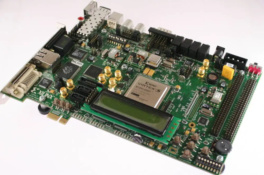
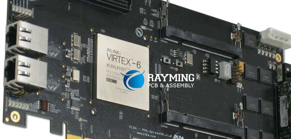
Xilinx Virtex series FPGAs are among the most advanced and widely used FPGAs in the industry. They provide very high capacity, performance, and extensive features for addressing the requirements of the most complex digital designs.

Overview of Xilinx Virtex FPGAs

The Virtex family is Xilinx’s flagship FPGA offering for high-end applications demanding very high capacity, performance, and bandwidth. Key characteristics of Virtex FPGAs include:

  • Advanced FPGA architecture based on SRAM configuration technology
  • High density of programmable logic cells and I/Os
  • Extensive clock management and interconnect capabilities
  • Advanced embedded features including high-speed transceivers, DSP blocks, block RAMs, PCIe, Ethernet
  • Sophisticated development software and IP support
  • Proven in a wide range of applications from wired and wireless infrastructure to aerospace and defense systems
  • Manufactured in state-of-the-art technology down to 7nm FinFET process
  • Available in high-reliability space-grade and industrial grade temperature versions
  • The top-end Virtex series competes with Intel (formerly Altera) Stratix FPGAs for leadership in FPGA capabilities

The major product families within the Virtex series over its two-decade evolution are: Virtex, Virtex-II, Virtex-4, Virtex-5, Virtex-6 and Virtex UltraScale. Each generation has pushed FPGA technology boundaries to deliver exponentially greater logic capacity, bandwidth, and features.

FPGA Overview

To better understand Virtex FPGAs, it is helpful to first briefly introduce FPGA technology.

What is an FPGA?

An FPGA or field programmable gate array is an integrated circuit chip containing three key programmable elements:

  1. Configurable Logic Blocks (CLBs) โ€“ Basic building blocks to implement digital logic gates and functions
  2. I/O Blocks โ€“ Periphery blocks providing input/output connectivity
  3. Programmable Interconnects โ€“ Routing paths between logic and I/O blocks

Structure of an FPGA (Image source: ResearchGate)

The FPGA can be programmed to perform desired functions by configuring the logic blocks and then interconnecting them with wires routed through the programmable routing matrix. This field-programmability offers immense flexibility compared to fixed-function ICs like ASSPs.

FPGA Fabric

The core of an FPGA is its fabric consisting of:

Configurable Logic Blocks (CLBs) โ€“ Made of small Look-Up Tables (LUTs) and flip-flops that can be user-programmed to implement logic functions, arithmetic operations, and memory elements. CLBs are arranged in an array and repeated across the FPGA.

Programmable Interconnects โ€“ Channels of horizontal and vertical routing tracks spanning the CLB array. Programmable switches connect the wiring tracks in flexible ways for routing signals between CLBs and I/O blocks.

I/O Blocks โ€“ Located at the periphery, these contain programmable I/O drivers/buffers to communicate signals off-chip. Some I/Os can also perform basic logic.

FPGA Configurable Logic Block structure (Image source: ResearchGate)

In addition to the generic fabric, FPGAs incorporate dedicated hardware blocks like block RAMs, DSP slices, clock management, PLLs, high-speed transceivers and more depending on the model.

FPGA Configuration

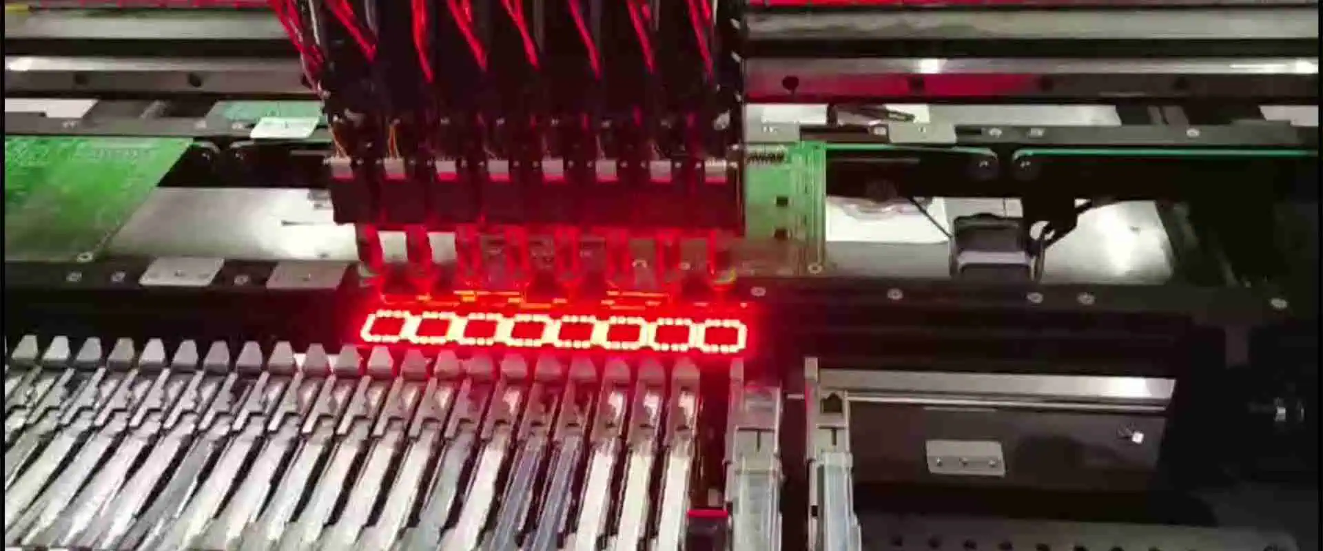
FGPAs use static RAM technology for configuration and programming. The SRAM cells control all the programmable switches and multiplexers in the CLBs, routing fabric, and I/Os. When powered on, an external memory device loads configuration data into the SRAM which programs the FPGA with the required logic and interconnects.

Evolution of Xilinx Virtex Series

The Virtex FPGA series has constantly pushed the technology envelope over two decades to achieve exponential increases in capacity and performance:

Virtex (1996)

  • First commercial FPGA with 1 million system gates
  • Up to 96 configurable logic blocks (CLBs)
  • On-chip RAM for distributed memory
  • High speed I/O up to 330 MHz

Virtex-II (2000)

  • Up to 9 million system gates capacity
  • Enhanced CLBs with built-in adders and WYSIWYG design
  • Up to 3.2 Gbps serial transceivers
  • Advanced power management features

Virtex-4 (2004)

  • 65nm process enabled up to 200K logic cells
  • DSP slices and 36 Kb block RAM for advanced embedded features
  • Multi-gigabit serial transceivers up to 11.2 Gbps
  • PCI Express Endpoint compliance

Virtex-5 (2006)

  • 40nm process for up to 330K logic cells and 69 Mb RAM
  • High-performance DSP48E slices
  • Multi-gigabit serial transceivers scaled to 6.5 Gbps
  • Next generation PowerPC in hard IP blocks

Virtex-6 (2009)

  • 40nm process with 1.7 billion transistors delivering two million logic cells
  • Serial transceivers operating up to 11.8 Gbps
  • Advanced power optimization techniques

Virtex UltraScale (2014)

  • Leading-edge 20nm process with up to 8.4 million logic cells
  • UltraRAM blocks for data buffering up to 432 Mbits
  • GTH transceivers up to 32.75 Gbps
  • Integrated 100G Ethernet solutions

This steady progression in integrating more advanced programmable logic resources and faster I/O bandwidth has made Virtex FPGAs exceptionally capable platforms for addressing highly demanding application needs.

Virtex FPGA Architecture

Xilinx Artix 7
Xilinx Artix 7

Virtex FPGAs have incorporated innovative architectural features to optimize performance, power efficiency, reliability, embedded functionality, signal processing capabilities and development productivity over successive generations.

Logic Fabric

The foundation of Virtex FPGAs is an array of highly flexible Configurable Logic Blocks (CLBs) containing LUTs, flip-flops, multiplexers, arithmetic carry chains and more. LUTs can implement any logic function of inputs. The spectrum of logic designs that can be mapped to the CLB array is immense. Surrounding the logic fabric are high-bandwidth I/O blocks and power/clock distribution networks.

Routing Architecture

Equally important is the programmable routing architecture that determines interconnect performance and efficiency. Virtex FPGAs utilize:

  • Multiple segmented routing channels spanning CLB rows and columns
  • An abundance of tracks to minimize congestion
  • Diverse length lines – short connects, hex lines, long lines, global networks
  • Low-skew global clocks distributed in balanced H-Trees
  • Fast carry chains for arithmetic operations

This flexible routing allows complex designs with high fanouts and clock frequencies to be implemented.

Embedded Block RAM

On-chip block RAMs provide large distributed memory for data buffering and look-up tables. Virtex UltraScale+ FPGAs have up to 68 Mb of UltraRAM blocks that can operate at speeds over 500 MHz.

DSP Slices

Hard DSP slices allow high-speed arithmetic like multiply-accumulate to be performed without consuming logic fabric. Virtex UltraScale+ incorporates up to 7680 DSP slices capable of up to 27 x 27 = 729-bit multiplications.

High-Speed I/O

Virtex chips feature gigabit-speed serial I/O transceivers for interfacing to the latest optical, networking and memory technologies. The current Virtex UltraScale+ has GTY transceivers operating up to 32.75 Gbps.

Hard IP Blocks

Dedicated hardware for common functions like PCIe, Ethernet, processors, memory/bus interfaces, video codecs have been integrated over generations. This improves performance and saves logic resources.

Advanced Power Management

Extensive power saving techniques like fine-grained clock gating, power domains, low voltage operation, optimized logic structures are employed. Virtex UltraScale+ consumes as low as 100 ฮผW per logic cell.

Configuration Infrastructure

Virtex leverages high-speed configuration ports, encryption, SEU immunity, partial reconfiguration and remote updates to deliver secure and reliable in-field programmability.

Virtex FPGA Device Offerings

Within each Virtex family, a range of models with different logic, I/O and transceiver capacities are offered targeting diverse applications. Some examples:

Virtex UltraScale+ Product Selection Guide

Virtex UltraScale Product Selection Guide

This multitude of options allows matching the optimal Virtex FPGA model to application needs in terms of I/O bandwidth, logic capacity, power budget, cost etc.

Virtex FPGA Development Ecosystem

Xilinx offers sophisticated design tools and resources to harness Virtex FPGAs:

  • Vivado Design Suite โ€“ Leading edge integrated design environment (IDE) for synthesis, placement, routing, simulation, implementation, debugging
  • IP Catalog โ€“ Massive portfolio of pre-optimized logic cores, interfaces, software drivers
  • Reference Designs โ€“ Proven design templates to accelerate development
  • Development Boards โ€“ Range of evaluation boards to prototype and test designs
  • System Generator โ€“ DSP design tool to integrate Xilinx MATLAB and Simulink
  • High-Level Synthesis โ€“ Transform C/C++/OpenCL code to optimized RTL
  • Domain-Specific Solutions โ€“ Solutions for key markets including data centers, automotive, vision systems
  • Designer Community โ€“ Active user community and technical support

Leveraging these software tools and resources is key to shorten time-to-market, enhance design productivity and fully harness the capabilities of Virtex FPGAs.

Applications of Virtex FPGAs

The enormous capacity, flexibility and performance of Virtex FPGAs make them ideal accelerators for diverse applications:

Data Center Compute/Networking

Implementing algorithms like machine learning inference or genomic sequencing in hardware on FPGAs massively speeds up throughput compared to software. Virtex FPGAs are deployed in data centers by cloud companies like Microsoft and Amazon. High-speed networking gear also relies on Virtex transceivers.

Wireless Base Stations

Virtex enables software-defined radio, digital pre-distortion, forward error correction and baseband processing for 4G/5G wireless infrastructure.

Automotive/ADAS

Sensor fusion, computer vision, neural networks for autonomous vehicles can be accelerated using Virtex while meeting ASIL requirements.

Test and Measurement

High-speed interfaces like JESD204 used in semiconductor testers are implemented on Virtex FPGAs. Real-time processing of wideband signals for defense testing also utilizes Virtex.

Imaging Systems

High resolution image signal processing at very high data rates is made possible by Virtex FPGAs. Applications include medical imaging, optics, video surveillance etc.

Aerospace and Defense

Virtex devices meet DO-254 certification for avionics. Radar, software-defined radio, video analytics are example mission-critical applications.

Scientific Research

The reconfigurability of Virtex FPGAs allows creating application-specific processing architectures like those used in astronomy and particle physics experiments.

This versatility to address diverse computation and I/O-intensive applications has made Virtex the gold standard FPGA for accelerating real-world systems.

Conclusion

Xilinx Virtex series FPGAs represent the pinnacle of programmable logic technology with very high logic density, bandwidth, embedded feature sets and robust development ecosystems. They empower designers to implement customized hardware architectures for meeting the changing demands of compute/IO-intensive applications in fields ranging from data center to defense. With ongoing innovations like 3D-IC packaging and software-defined development, Virtex FPGAs will continue breaking barriers in FPGA capabilities and user productivity.

FAQs

What are the main differences between Virtex and Spartan FPGAs?

Virtex is the flagship high-end FPGA series while Spartan targets lower cost applications. Virtex offers higher logic capacity, more features like transceivers, hardened IP, memory bandwidth. Spartan has smaller density and optimized for cost/power-sensitive designs.

How are the different Virtex families related to each other?

Virtex families like Virtex-4, Virtex-5, Virtex-6 etc represent successive generations built with more advanced process technology, architecture upgrades and added features. Virtex UltraScale is the latest generation providing massive capacity, performance and integration.

What process technologies are used to manufacture Virtex FPGAs?

Leading edge manufacturing processes like 7nm FinFET are used to fabricate Virtex chips. Each generation shifts to smaller geometries allowing greater transistor density and performance. Advanced packaging like 2.5D is also utilized.

What is unique about Virtex compared to FPGAs from other vendors?

Virtex differentiators include very high logic and IO bandwidth, abundant hard IP blocks, advanced DSP optimized fabric, extensive software/IP ecosystem, vast application experience and technology leadership through rapid innovations.

What are some alternatives to using Virtex FPGAs?

Alternatives include lower-cost FPGAs like Spartan or competition, GPUs for acceleration, ASICs for custom hardware, CPUs+DSPs or other programmable logic/SoC devices. Virtex provides best in class FPGA capabilities on critical metrics.

Everything about Xilinx Virtex FPGA Product Line

Integrated circuits are a vital aspect of electronic and electrical systems. It not only proves pivotal in designing electronics but ensures their proper functioning. Consequently, you will find ICs in amplifiers, computer memory, video processors, microprocessors, switches, etc. However, like all other industry-revolutionizing products and product lines, it is impossible to talk about and understand ICs fully without canvassing the Virtex FPGA. So what is it all about?  

Virtex represents a flagship FPGA product family established by Xilinx. It includes models and configurations that are optimized for diverse applications. The Xilinx Virtex encompasses different families. It includes Virtex-E, Virtex-II, Virtex-4, Virtex-5, Virtex-6, and Virtex-7. Virtex-7 (3D), Virtex UltraScale, Virtex UltraScale+, and SoC finalize the product group.

Virtex FPGA series rely on the CLBs (configurable logic books). Each CLB equates to several ASIC gates and comprises several slices which have different construction architecture between families. Virtex FPGA also possesses other series, including Artix (low-cost), Kintex (mid-range), and Spartan low-cot series.

Virtex has diverse product series with plenty of families. Therefore, this article will focus on the Virtex FPGA product series. Let us get to it right away, shall we?

Xilinx Virtex FPGA

Virtex FPGAs from Xilinx have a huge industry reputation for their market impact and innovation. The Virtex FPGA gets programmed in special hardware description languages like Verilog or VHDL and utilizes the Vivado or Xilinx design suite. Its architectural design encompasses an I/O block that controls output and input pins in the Virtex chip. Such a design proves instrumental in supporting a myriad of signaling standards.

All the pins are the default for the input mode, implying high impedance, with I/O pins getting assembled into I/O banks that feature every bank supporting a different voltage. Moreover, besides configurable FPGA, the Virtex FPGAs also entail fixed-function hardware for memories, multipliers, microprocessor cores, ECC, and FIFO logic, besides DSP bocks. But it does not stop there; it encompasses Ethernet high-speed serial transceivers, MAC blocks, and PCI express controllers.

If you, therefore, need to purchase a Virtex FPGA product series from Xilinx, it helps to consider certain aspects. For instance, it will come in handy to comprehend the different series for each product line under the Xilinx Virtex FPGA product line, their corresponding features, and their suitability to your area of application. Additionally, other aspects such as costs, your PCB contract manufacturer, PCB design needs, etc., have to be factored in.

Xilinx Virtex-II

The Virtex-II FPGA family was developed for high-performance functions encompassing low to high-density designs and basing everything on its customized modules and IP cores. It delivers a comprehensive solution for wireless networking, telecommunication, DSP, and video applications. It entails DDR, LVDs, and PCI interfaces. The advanced Virtex-II architecture, besides the 0.15 ยตm / 0.12 ยตm CMOS 8-layer metal procedure, ensures optimization for low-power, high-speed operations. Additionally, it combines many flexible attributes and densities that go up to ten million system gates. Consequently, it reinforces programmable logic design abilities besides proving a fantastic option in mask-programmed arrays.

  • Input/Output Blocks

The IOBs prove programmable besides having three categorizations. It includes an input block complete with DDR or single-data-rate register, output block with DDR register, and a bidirectional block combining output and input configurations.

  • CLBs

It is a resource that encompasses two 3-state buffers and four slices. Each has two function generators, arithmetic logic gates, two storage elements, a fast carry look-ahead chain, large multiplexers, a horizontal cascade gate, and extensive function ability.

  • Global Clocking

The global clock multiplexer and DCM buffers give a comprehensive solution in the design of high-speed clocking schemes. The Virtex-II possesses up to twelve DCM blocks, with every DCM capable of being deployed to eradicate clock distribution delays.

  • Routing Resources

All the Virtex-II elements, such as CCLB, IOB, etc., use a similar interconnect scheme with a single global routing matrix access. A total of sixteen global clock lines exist, with each quadrant having eight.

  • Configuration

Virtex-II devices get configured through a process of loading data to the internal configuration memory. It uses one among the five: slave-serial, slave selectMAP, master-serial mode, master SelectMAP, and boundary-scan modes. Additionally, a DES (Data Encryption Standard) decryptor proves available.

Xilinx Virtex-2Pro

It comes as an FPGA design based on customized modules and IP cores. The Virtex-II Pro adds a PowerPC CPU and multi-gigabit transceiver in its architecture. Therefore, it offers a comprehensive solution to wireless, telecommunication, video, wireless, DSP, and networking applications. The industry-leading 0.13 ยตm CMOS nine-layer copper process, besides the Virtex-II Pro architecture, ensures optimization for high-performance designs featuring a divergent density range. Additionally, it mixes a myriad of IP cores and flexible attributes, which enhance the programmable logic design abilities. Consequently, it is an excellent option to mask programmed gate arrays.

  • IOBs

The input/output blocks come programmable and with diverse categorizations. The registers prove level-sensitive or edge-triggered D-type flip-flops latches. Whatโ€™s more? The IOBs support single-ended I/O standards like LVCMOS and LVTTL, PCI-X compatible, PCI compliant, and GTLP and GTL compliant.

  • PowerPC 405 Processor Block

The PPC405 RISC CPU executes instructions at sustained rates of a single instruction per cycle. Additionally, data cache and on-chip instruction limit design complexity besides enhancing system throughput. Features include storage control, PowerPC RISC CPU, a virtual memory management unit, debug support, and OCM controllers.

  • CLBs

The configurable logic blocks possess two 3-state buffers and four slices. Each slice proves equivalent to the next and has two function generators, arithmetic logic gates, two storage elements, large multiplexers, a Horizontal cascade gate or chain, and wide function ability. Here, the function generators also prove configurable.

  • Routing Resources

Elements such as the CLB, IOB, block SelectRAM+, DCM, and multipliers utilize one scheme besides a similar global routing matrix. Timing models also get shared, and this improves the predictability aspect of high-speed design performance.

  • Configuration

It proves similar to all other Virtex families, especially on the mode of bitstream loading. However, the DES ensures the security of the bitstream once loaded on the chip.

  • Integrated Logic Analyzer and Readback

Another key element of the Virtex-II pro is that its stored configuration data can be read back in instances requiring verification.  Consequently, it allows for a seamless debugging process whenever necessary.

Xilinx Virtex-4

Similar to other Virtex series, the Virtex-4 from Xilinx combines the ASMBL architecture with a wide-ranging variety of flexible attributes. It enhances the programmable logic design abilities, ranking it a powerful option to the ASIC tech. Virtex-4 FPGAs encompass three subfamilies in LX, SX, and FX and thus provides multiple attribute options and combinations that can address complex applications. It has a hard-IP core block encompassing the PowerPC processors, 622 Mb/s to 6.5 Gb/s serial transceivers, tri-mode Ethernet MACs, dedicated DSP slices, source-synchronous interface blocks, and high-speed circuitry in its clock management. A standard Virtex-4 FPGA building block improves the ones found in renowned Virtex, Virtex-E, Virtex-II Pro, Virtex-II, and Virtex-II Pro X families. Therefore, it implies that earlier generation designs can prove upward compatible.  

The Virtex-4 devices get fabricated on an advanced 90nm copper procedure by deploying 300 mm wafer technology.

  • Configuration

Virtex-4 devices get configured through a loading process of the bitstream to the ICM or internal configuration memory. It completes this through slave-serial, master SelectMAP, slave selectMAP, master-serial, and boundary-scan mode. It also features an optional 256-bit AES decryption that gets supported on-chip. Consequently, it provides intellectual property (IP) security.

  • Block RAM

It has a block RAM resource of 18 Kb true dual-port RAM, and it is programmable from 16K x 1 to 512 x 36, width and depth configurations. Additionally, every port is fully independent and synchronous. It thus offers three โ€œread-during-writeโ€ modes. Whatโ€™s more? Block RAM proves cascadable and should carry out large embedded storage blocks. Further, the back-end pipeline register, built-in FIFO support, byte write, and clock control circuitry prove but only a few features supported within the Virtex-4 FPGA

  • CLBs

For the Virtex-4 FPGAs, the CLB resource comprises four equivalent slices. Each has two function generators, arithmetic logic gates, two storage elements, and larger multiplexers, besides a quick carry look-ahead chain. The Virtex-4 FPGAโ€™s function generators prove configurable as 4-input LUTs. Two CLB slices can get their LUTs configured to become 16-bit distributed RAM or 16-bit shift registers. Its two storage elements can also prove level-sensitive or edge-triggered D-type flip-flops latches.

  • I/O Blocks

Input/output blocks come programmable with different categorizations. Further, the IOB registers can either prove level-sensitive latches or edge-triggered D-type flip-flops. Another possibility entails configuring the DCI I/O attribute to offer on-chip termination, especially for every single-ended I/O and differential I/O standard.

  • Routing Resources

Components on the Virtex-4 devices deploy a similar interconnect scheme besides a similar global routing matrix access. Additionally, the timing models get shared and thus, enhances the performance prediction for the high-speed designs.

Xilinx Virtex-5

The Virtex-5 FPGAs deploy the second-generation ASMB column-based architecture. It possesses five sub-families, with every sub-family having a distinct features ratio regarding meeting the needs of diverse and advanced logic designs. The FPGA family contains the most progressive, high-performance logic fabric. It also has plenty of hard-IP system-level blocks that include the powerful 36-Kbit block RAM and second-generation 25 x 18 DSP slices. It also contains the SelectIO technology (including built-in digitally-controlled impedance), system monitor functionality, and the ChipSync source-synchronous interface blocks. Further, the Virtex-5 FPGA also features a superior clock management tile complete with an integrated PLL and DCM clock, innovative configuration options, and generators.

  • Configuration

The Virtex-5 devices get configured through a bitstream loading process into the internal configuration memory. It can become a reality through the deployment of the following modes. The slave-serial, master-serial, slave selectMAP, master SelectMAP, boundary-scan, SPI, and BPI-down/BPI-up modes. Additionally, it supports options such as 256-bit AES bitstream decryption, multi-bitstream management, and the auto-detection of the parallel configuration bus width. Whatโ€™s more? It can also support parallel daisy chains and ECC and CRC configurations.

  • System Monitor

The system monitor on the Virtex FPGAs from Xilinx is a vital building block for high reliability or availability infrastructure. It enhances the monitoring of the on-chip FPGA physical environment besides its immediate system surroundings. It has several subfamilies, with each member possessing a system monitor block. The Virtex-5 System Monitor is built using a 10-bit 200kSPS Analog-to-Digital Converter (ADC).

An ADC is instrumental in digitizing several on-chip sensors in providing information concerning the FPGAโ€™s physical environment. The on-chip sensors entail a power supply and temperature sensors. External environmental access gets facilitated by several external analog input channels. Such analog inputs come general purpose and, thus, can get deployed in digitizing a diverse variety of voltage signals.

In addition, support gets provided for true differential, bipolar, and unipolar input schemes. Consequently, full access to external channels and on-chip sensors is guaranteed through the JTAG TAP, which allows the present JTAG infrastructure located on the board (PC) to be utilized for advanced diagnostic and analog tests during development and post-deployment. The System Monitor often proves fully operational before the FPGA configuration and after powering it up. Further, the System Monitor never needs an obvious instantiation in the design to access aspects such as basic functionality. Consequently, it permits the System Monitor utilization during the latter stages of the design cycle.

  • Routing Resources

Every component in the Virtex-5 device deploys a similar interconnect scheme besides single access to the universal routing matrix. Additionally, the design of the CLB-to-CLB routing provides a comprehensive connectivity set in very few hops. Since timing models get shared, the prediction of the high-speed designs gets enhanced.

  • Global Clocking

The global-clock multiplexer buffers and the CMTs offer a comprehensive solution for the design of high-speed clock networks. Every CMT possesses a single PLL and two DCMs. The PLL and DCM can be deployed independently. The Virtex-5 contains up to six CMT blocks and thus offers a total maximum of eighteen clock generator elements. Each DCM gives a familiar clock generation ability. However, when it comes to the generation of deskewed external or internal clocks, every DCM can get utilized to eliminate the delay in clock distribution. It also offers 270ยฐ, 180ยฐ, and 90ยฐ phase-shifted output clock versions. The Virtex-5 FPGA has PLL to augment the capability of the DCM. Such a clock offers extra synthesis and reference clock jitter filtering options. What’s more? It possesses 32 global-clock MUX buffers complete with a differential clock tree to minimize the duty cycle distortion besides the jitter.

  • Boundary Scan

The boundary-scan associated data registers and instructions support a typical configuration and access methodology for Virtex-5 devices. Consequently, it allows for conformation and compliance with IEEE standards 1532 and 1149.1.

  • Block RAM

The Virtex 36 Kbit, dual-port RAM block resources, come programmable, especially from 32K x 1 to 512 x 72, in diverse width and depth configurations.  Additionally, every 36-Kbit block can get configured to function as two autonomous 18-Kbit dual-port RAM blocks. Remember, every port is fully independent and synchronous and thus provides three “read-during-write” modes.

  • CLBs

The configurable logic block resource entails two equivalent slices. Every slice has four storage elements, a similar number of function generators, large multiplexers, arithmetic logic gates, and a quick carry look-ahead chain. The function generators can get configured as dual-output 5-input or 6-input LUTs.  Additionally, the storage elements (four) can get configured into level-sensitive or edge-triggered D-type flip-flop latches.

  • I/O Blocks

The Virtex-5 FPGAs have programmable IOBs with diverse categorizations. The DCI (digitally controlled impedance I/O attribute can get configured to give on-chip termination.  

Xilinx Virtex-6 FPGA

Xilinx Virtex-6 FPGA

The series comes as a programmable silicon foundation for TDPs (targeted design platforms) to deliver integrated hardware and software components. Consequently, it enables designers to concentrate on innovation immediately after their cycle of development starts. The series deploy the ASMBL column-based architecture besides possesses several individual sub-families.

It has countless built-in system-level blocks. Such attributes allow the logic designers to develop the highest functionality and performance levels in the FPGA-based system. The Virtex-6 FPGA gets built using the 40 nm cutting-edge copper process tech. It also proves a programmable option when it comes to custom ASIC tech. Virtex-6 FPGA provides a top solution in addressing the requirements of high-performance DSP, logic, and embedded system designers, primarily those with unprecedented connectivity, logic, soft microprocessor, and DSP capabilities.  

  • Configuration

Virtex-6 FPGA has a customized configuration and stores it in an SRAM-type internal latch. The configuration bits can range from 26Mb to 177Mb based on the device’s size but disregard the particular user-design implementation unless you deploy the compression mode.

Additionally, the configuration mode proves volatile and requires reloading every time the FPGA gets powered up. It is possible to reload this storage at any moment, provided you pull the PROGRAM_B pin low.  

Bit-serial configuration can come as either master serial mode or the slave serial mode. The master serial mode infers when the FPGA creates the CCLK signal, while the slave serial mode implies when the external configuration source of data clocks the FPGA. A standard configuration process encompasses the execution of the sequence as follows.

  • It detects power-up or PROGRAM_B during Low
  • It clears the entire configuration memory
  • A sampling of the mode pins gets completed to establish the configuration mode. It can prove slave or master, parallel or bit-serial, or even bus width.
  • It loads the configuration files and begins with the bus-width detection pattern, synchronization word, checking for the correct device code before ending with the CRC (cyclic redundancy check) of the whole bitstream.
  • Start-up then implements a user-defined events sequence that releases the internal presser or reset of flip-flops, optionally waits for the PLLs or phase-locked loops to lock or/and the matching of the DCI, besides activating the drivers’ output, and transitioning the DONE pin to High.
  • CLBs, LUTs, and Slices

It is possible to configure the LUT (look-up table) of Virtex-6 FPGAs as either two 5-input LUTs with isolated outputs but possessing common addresses or one 6-input LUT with a singular output. Optional registration of every LUT output can get carried out in a flip flop. Consequently, four such LUTs, together with their arithmetic, carry logic form, multiplexers, two slices, and eight flip flops from the CLB. It is also possible to optionally configure four flip flop slices as latches, provided that you configure each flip flop slice per LUT. However, such an occurrence demands that the rest (four flip-flops in the slice) stay unused.    

  • Clock Management

Every Virtex-6 FPGA contains up to nine CMTs (clock management tiles), each comprising two MMCMs (mixed-mode clock managers) that prove PLL-based. It features attributes such as phase-locked loop, MMCM programmable features, and clock distribution.

  • Block RAM

Every Virtex-6 FPGA contains a range of 156 to 1064 dual-port block RAMs. Remeber, each port block stores 36 Kbits. Additionally, each RAM block possesses two independent ports with nothing in common other than the data stored. It features synchronous operation, error detection, and rectifier, besides a programmable data width.

  • Digital Signal Processing

DSP applications deploy numerous binary accumulators and multipliers, best executed in devoted DSP slices. Every Virtex-6 FPGA has plenty of dedicated, low-power, and full-custom DSP slices, and these combine small size with high speed while retaining the flexibility of the system design.

  • I/O (Input/Output)

The amount of I/O pins differs and can range from 240 to 1200 based on the package size and device. Every I/O pin can get configured to comply with a hefty amount of standards. Besides the supply pins and other dedicated configuration pins, every package pins possess similar I/O capabilities that can only get constrained by specific banking rules.

I/O pins get organized in banks of forty pins. Each bank contains one standard output supply-voltage pin that powers specific input buffers. An important consideration for I/O pins includes understanding their electrical characteristics, digitally controlled impedance, and corresponding I/O logic.

  • System Monitors

All Virtex-6 FPGAs have system monitor circuits that provide power supply and thermal status information. The sensor outputs get digitized with a 10-bit 200kSPS ADC. The system monitor by design consistently digitizes all the on-chip sensors output. Every recent reading (measurements) gets stored in devoted registers.

It is vital to note that the series does not end at the Xilinx Virtex-7. Other families within this product line exist and include Virtex-7 FPGA, Xilinx PROM, etc., to mention but a few.

Conclusion

Integrated circuits are vital for electronic systems and so do the Xilinx Virtex product lines. If you want to buy a relevant IC within this product range but are unsure what to settle for, you can always get guidance at RayMing PCB and Assembly. Customer care is one among many IC services we provide.

Xilinx Virtex Part Numbers List

  • XC7K325T-1FBG676C
  • XC7K325T-1FBG676C
  • XC7K325T-1FBG676CES9909
  • XC7K325T-1FBG676CES9910
  • XC7K325T-1FBG676CES9911
  • XC7K325T-1FBG676CES9912
  • XC7K325T-1FBG676CES9913
  • XC7K325T-1FBG676CES9919
  • XC7K325T-1FBG676I
  • XC7K325T-1FBG900C
  • XC7K325T-1FBG900CES9909
  • XC7K325T-1FBG900CES9910
  • XC7K325T-1FBG900CES9911
  • XC7K325T-1FBG900CES9912
  • XC7K325T-1FBG900CES9913
  • XC7K325T-1FBG900CES9919
  • XC7K325T-1FBG900I
  • XC7K325T-1FFG676C
  • XC7K325T-1FFG676CES9909
  • XC7K325T-1FFG676CES9910
  • XC7K325T-1FFG676CES9911
  • XC7K325T-1FFG676CES9912
  • XC7K325T-1FFG676CES9913
  • XC7K325T-1FFG676CES9919
  • XC7K325T-1FFG676CES9937
  • XC7K325T-1FFG676CESLAB
  • XC7K325T-1FFG676CESLAB1
  • XC7K325T-1FFG676I
  • XC7K325T-1FFG900C
  • XC7K325T-1FFG900CES9909
  • XC7K325T-1FFG900CES9910
  • XC7K325T-1FFG900CES9911
  • XC7K325T-1FFG900CES9912
  • XC7K325T-1FFG900CES9913
  • XC7K325T-1FFG900CES9919
  • XC7K325T-1FFG900CES9937
  • XC7K325T-1FFG900CESLAB1
  • XC7K325T-1FFG900I
  • XC7K325T-1FFG900I9924
  • XC7K325T-1FFG900I9927
  • XC7K325T-2FBG676C
  • XC7K325T-2FBG676CES9909
  • XC7K325T-2FBG676CES9910
  • XC7K325T-2FBG676I
  • XC7K325T-2FBG900C
  • XC7K325T-2FBG900CES9909
  • XC7K325T-2FBG900CES9910
  • XC7K325T-2FBG900I
  • XC7K325T-2FFG676C
  • XC7K325T-2FFG676CES9909
  • XC7K325T-2FFG676CES9910
  • XC7K325T-2FFG676CES9937
  • XC7K325T-2FFG676CESLAB1
  • XC7K325T-2FFG676I
  • XC7V2000T-1FLG1925CES9913
  • XC7V2000T-1FLG1925CES9915
  • XC7V2000T-1FLG1925CES9922
  • XC7V2000T-1FLG1925CES9937
  • XC7V2000T-1FLG1925CES9938
  • XC7V2000T-1FLG1925ES9921
  • XC7V2000T-1FLG1925I
  • XC7V2000T-2FH1761C
  • XC7V2000T-2FHG1761C
  • XC7V2000T-2FHG1761CES
  • XC7V2000T-2FHG1761CES9911
  • XC7V2000T-2FHG1761CES9913
  • XC7V2000T-2FHG1761CES9922
  • XC7V2000T-2FHG1761CES9937
  • XC7V2000T-2FHG1761CES9938
  • XC7V2000T-2FL1925C
  • XC7V2000T-2FLG1925C
  • XC7V2000T-2FLG1925CES
  • XC7V2000T-2FLG1925CES9911
  • XC7V2000T-2FLG1925CES9913
  • XC7V2000T-2FLG1925CES9922
  • XC7V2000T-2FLG1925CES9937
  • XC7V2000T-2FLG1925CES9938
  • XC7V2000T-G2FH1761E
  • XC7V2000T-G2FHG1761E
  • XC7V2000T-G2FL1925E
  • XC7V2000T-G2FLG1925E
  • XC7V2000T-L2FH1761E
  • XC7V2000T-L2FHG1761E
  • XC7K325T-2FFG900C
  • XC7K325T-2FFG900CES9909
  • XC7K325T-2FFG900CES9910
  • XC7K325T-2FFG900CES9937
  • XC7K325T-2FFG900CESLAB1
  • XC7K325T-2FFG900CESLAB2
  • XC7K325T-2FFG900I
  • XC7K325T-2FFG900I9926
  • XC7K325T-3FBG676E
  • XC7K325T-3FBG900E
  • XC7K325T-3FFG676E
  • XC7K325T-3FFG900C
  • XC7K325T-3FFG900E
  • XC7K325T-ESLAB
  • XC7K325T-FFG900
  • XC7K325T-L2FBG676E
  • XC7K325T-L2FBG900E
  • XC7K325T-L2FFG676E
  • XC7K325T-L2FFG900E
  • XC7K480T-1FFG1156C
  • XC7K480T-1FFG1156CES9919
  • XC7K480T-1FFG1156I
  • XC7K480T-1FFG901C
  • XC7K480T-1FFG901CES9919
  • XC7K480T-1FFG901I
  • XC7K480T-2FFG1156C
  • XC7K480T-2FFG1156I
  • XC7K480T-2FFG901C
  • XC7K480T-2FFG901I
  • XC7K480T-3FFG1156
  • XC7K480T-3FFG1156E
  • XC7K480T-3FFG901
  • XC7K480T-3FFG901E
  • XC7K480T-L2FFG1156
  • XC7K480T-L2FFG1156E
  • XC7K480T-L2FFG901
  • XC7K480T-L2FFG901E
  • XC7V2000T-1FH1761C
  • XC7V2000T-1FH1761I
  • XC7V2000T-1FHG1761C
  • XC7V2000T-1FHG1761CES
  • XC7V2000T-1FHG1761CES9911
  • XC7V2000T-1FHG1761CES9913
  • XC7V2000T-1FHG1761CES9915
  • XC7V2000T-1FHG1761CES9922
  • XC7V2000T-1FHG1761CES9937
  • XC7V2000T-1FHG1761CES9938
  • XC7V2000T-1FHG1761ES9921
  • XC7V2000T-1FHG1761I
  • XC7V2000T-1FL1925C
  • XC7V2000T-1FL1925I
  • XC7V2000T-1FLG1925C
  • XC7V2000T-1FLG1925CES
  • XC7V2000T-1FLG1925CES9911
  • XC7VX485T-2FFG1927CES9937
  • XC7VX485T-2FFG1930
  • XC7VX485T-2FFG1930CES9913
  • XC7VX485T-1FFG1157CES9915
  • XC7VX485T-1FFG1157CES9919
  • XC7VX485T-1FFG1158CES9915
  • XC7VX485T-1FFG1158CES9919
  • XC7VX485T-1FFG1761CES9913
  • XC7VX485T-1FFG1761CES9915
  • XC7VX485T-1FFG1761CES9919
  • XC7VX485T-1FFG1761CES9937
  • XC7VX485T-1FFG1761CESLAB
  • XC7VX485T-1FFG1927
  • XC7VX485T-1FFG1927CES
  • XC7VX485T-1FFG1927CES9913
  • XC7VX485T-1FFG1927CES9919
  • XC7VX485T-1FFG1927CES9937
  • XC7VX485T-1FFG1927CESLAB
  • XC7VX485T-1FFG1930CES9913
  • XC7VX485T-1FFG1930CES9915
  • XC7VX485T-1FFG1930CES9919
  • XC7VX485T-1FFG1930CES9937
  • XC7VX485T-2FFG1761CES9913
  • XC7VX485T-2FFG1761CES9937
  • XC7VX485T-2FFG1927CES
  • XC7VX485T-2FFG1927CES9913
  • XC7V2000T-L2FL1925E
  • XC7V2000T-L2FLG1925E

Xilinx Kintex-7 FPGAs technical database

Top 7 Pick and Place Assembly Supplier in Spain

pick and place machine for pcb assembly

The innovations that come with advancements in technology could go a long way to introduce new concepts in the manufacturing industry. This is already evident in the invention of the pick and place machines.

Today, these machines are used to facilitate the production of different kinds of things, including Printed Circuit Boards (PCBs).

In this article, we will talk about the relevance of the pick and place assembly machines in the PCB sector, the major suppliers of these machines in Spain, as well as some of the benefits of using the pick and place machines.

What is Pick and Place Machines Used for?

First things first โ€“ let us understand what pick and place machines are all about. This way, you will find it easier to understand the reason for the use of these machines in the production of Printed Circuit Boards (PCBs).

Pick and Place Machines are robotic machines that are used to place the Surface Mount Devices (SMDs) onto the Printed Circuit Boards (PCBs).

Pick and place machines are also known by many other names, such as Pick and Place Robots and Surface Mount Technology Component Placement Systems.

The Relevance of Pick and Place Machines in the PCB Market

FULL PCB MANUFACTURING Quote

There are many reasons why the manufacturers of Printed Circuit Boards (PCBs) use pick and place machines.

Here are some of those reasons:

1. Automation

This is the most common reason why PCB manufacturers choose to go for the pick and place machines. The process of designing and manufacturing circuit boards can be tasking most of the time.

This could also mean that the PCB manufacturer would have to employ more circuit board professionals to facilitate the PCB production process.

However, investing in a pick and place machine goes a long way to reduce the workload. The machine is fast and could go a long way to reduce the errors or defects in the circuit board production phase.

2. Pick and Place Machines Could Save Costs

Getting one pick and place machine could help a PCB manufacturer drastically cut down on costs.

This is because the machine could do the work of two or more PCB experts at once, thereby, saving the manufacturer some money.

3. Machine Learning (MIL)

One of the biggest relevance of using pick and place machines in the PCB manufacturing phases is because of the Machine Learning (ML) capabilities.

This is because the pick and place machines could โ€œlearnโ€ more about the PCB production process.

With the combination of Artificial Intelligence (AI), the pick and place machine can be modeled to โ€œlearnโ€ and โ€œrememberโ€ a particular sequence in the PCB production phase.

Over time, the machines would be able to replicate the same in subsequent PCB tasks.

Where to Get Pick and Place Assembly Machines

You now know the relevance or importance of pick and place assembly machines in the Printed Circuit Board (PCB) production process.

The next step is to find the best manufacturers or suppliers of these machines. It will interest you to know that you can get some of the best pick and place machines in Spain.

Yes, there are several Spanish pick and place machine manufacturers that you would like to patronize.

Here are seven (7) of the leading pick and place machine manufacturers in Spain:

1. Surtel

pcb pick and place

Surtel or Surtel Electronica is the first pick and place assembly machine supplier on our list. The company has numerous years of experience and extensive experience in the production of pick and place assembly machines.

We have made series of background checks on the company and found out that it has a lot to offer, as far as the DIY SMT pick and place machines are concerned.

Huge Facilities

Surtel has the facilities to accommodate the different solutions the company has to offer to the PCB market.

The facilities measure 6,000 square meters, giving the manufacturer enough room to go about the business of manufacturing and distributing pick and place robots.

The other aspect of the huge facilities is the insertion rate of the 500,000 components per hour. With this, you can be confident that the pick and place PCB assembly equipment you are getting from this manufacturer would be worth the money.

High Technology

Innovation is at the core of all that Surtel has to offer. Surtel Electronica is committed to the continuous improvement of the pick and place assembly equipment production. This is part of the companyโ€™s efforts at ensuring that the PCB factories buying those machines get value for their money.

Besides, Surtel Electronica doesnโ€™t cut down on quality. Instead, the company prioritizes the use of its high technology and continuous innovation and best practices to offer the best quality pick and place machines.

Extensive Market Coverage

Surtel Electronica, is no doubt, one of the leading suppliers of pick and place machines in Spain and beyond.

This is because of the extensive market coverage used by the company. Currently, Surtel Electronic has strategic locations near the Mediterranean Coast and in Andalusia.

These locations help the company to be closer to the target market in the sense that Surtel Electronica uses them to keep its tie closer to the major pick and place machine retailers in Europe.

Website: https://www.surtel.es/en/

2. Electronic Advanced Circuits

pick and place assembly

Here is the second Spanish pick and place machine manufacturer that you would be interested to patronize.

Many factors make Electronic Advanced Circuits one of the best pick and place robotics manufacturers in Spain.

These are some of the reasons or advantages of sourcing your next pick and place machines from this supplier:

Single PCB Supplier

Have you always wanted to source all your PCB assembly solutions from the same place? Shopping at the same place can help you get things cheaper, and makes it easier for you to get solutions to any need you may have in the same place.

This is exactly what Electronic Advanced Circuits offer. This Spanish pick and place machine supplier believes in providing all the PCB-related solutions at a go. Hence, it opts to be the single PCB supplier for all kinds.

Imagine how thrilling it is to have your technical, commercial, and logistical PCB needs to be matched to the capabilities of a circuit board equipment manufacturing plant.

Electronic Advanced Circuits excels at this because this pick and place machine manufacturer can conveniently find logistical and technical solutions to any PCB complexities you may have.

Superior Quality

Any pick and place machine you are looking to buy should offer superior quality. With this, your customers will get value for their money.

This is also one of the reasons why many PCB manufacturers prefer to source their pick and place robots from Electronic Advanced Circuits because this supplier offers superior quality equipment.

The quality of the pick and place PCB assembly equipment is bolstered by the fact that the supplier has one of the best teams in the world. The Electronic Advanced Circuitโ€™s team has extensive knowledge of pick and place machines. This knowledge is leveraged to create and offer unmatched pick and place machine manufacturing and distribution solutions.

Besides, the company continually makes relevant investments towards the improvement of the pick and place machine services. For example, it invests in both the Research and Development (R & D), as well as the latest machinery. This, when combined with the latest advances in the use of the Printed Circuit Board (PCB) Technology gives the company an edge.

Multiple Use Cases

One of the primary considerations you need to make when choosing a pick and place machine is the type of Printed Circuit Boards (PCBs) that can be used on the machine.

The pick and place assembly machines supplied by Electronic Advanced Circuits are not only versatile but also efficient.

Ideally, you can use these machines to design and manufacture different kinds of circuit boards, including:

Website: https://www.eac-eu.es/

3. EIIT

pick and place pcb assembly

EIIT is a Madrid-based engineering company that has been designing and supplying different kinds of testing equipment.

EIIT focuses on four (4) different business areas and has been doing well in those areas. These areas are:

  • Special Test Equipment, which focuses on the production of equipment that tests the functionality of engineering products.
  • Solutions Equipment & Partnership is a medium through which EIIT collaborates with other relevant brands in the global engineering sector.
  • EIIT also has the Aeronautics sector that has to do with the production of solutions for the aerospace and defense industries.
  • Finally, EIIT has the Automation Systems, which is where you will find the pick and place machine for sale.

The EIIT Automation Systems

Automation Systems are the sector of the business operations offered by EIIT. Here, PCB factories from different parts of the world contact EIIT to find out the latest pick and place machine for sale.

These Automation Systems are designed to help these circuit board manufacturers to get a flexible pick and place assembly solutions.

Among the solutions offered here are the provision of the necessary services, ranging from the conceptual design of the pick and place machines to the planning and development. EIIT also offers installation and support services to help PCB manufacturers get the most out of their pick and place PCB assembly equipment.

Pick and Place PCB Assembly Equipment Turnkey Solutions

Only a few pick and place machine suppliers offer turnkey solutions. This is one of the factors that separate EIIT from its competitors.

The turnkey solutions offered by EIIT go a long way to help PCB factories looking to buy the pick and place PCB machines with lots of options to choose from.

First, the turnkey solutions are an avenue for PCB factories to demand specific features and functions to be included in the machines.

Second and most important, EIIT offers the PCB factories the opportunity to go for custom-made solutions that border on the design, commissioning of specific systems, and flexible production lines for the pick and place PCB assembly machine.

As a PCB factory, you may also want to demand a prototype pick and place machine so you can have an idea of what the final product would look like.

Besides, EIIT is open to integrating different technologies that bolster pick and place robotics production into all of its systems.

Website: https://www.eiit.com/en/eiit/

4. Alter Technology

Alter Technology is another Spanish pick and place machine manufacturer. The company specializes in the provision of micro and optoelectronics services in the areas of engineering, assembly, procurement, and testing.

Target Market

The pick and place PCB machines supplied by Alter Technology are designed to be used in space and harsh environments.

Client Satisfaction

The satisfaction of the clients or PCB factories is one of the reasons why you want to purchase pick and place machines from the company.

Customer satisfaction is facilitated via the use of advanced applications, superior technology, and breakthrough innovations.

Turnkey Solutions

Alter Technology also offers turnkey pick and place PCB machine assembly solutions. These solutions are targeted at PCB factories that require a few touches.

With turnkey solutions, PCB factories from different parts of the world can make special requests for customized pick and place machines.

Some of the turnkey solutions offered by the company are:

  • Packaging
  • Dice probing
  • Assembly
  • Front-end engineering test
  • Wafer sawing
  • Wafer probing
  • Final test

Website: https://www.altertechnology-group.com/en/home/

5. Europlacer

Are you looking for a pick and place machine supplier that designs the machines to be flexible? If so, Europlacer is the supplier you are looking for.

This is one of the best pick and place machine suppliers, not only in Spain but also in many other parts of the world. The supplier has an extensive distribution network that covers Spain, the Americas, Asia Pacific, the United Kingdom, Italy, France, China, and Germany.

Here are some of the reasons why Europlacer could be the best pick and place machine supplier in Spain:

Adaptable Machines

Asides from the flexibility, the pick, and place equipment supplied by Europlacer is also adaptable. The adaptability of these machines means that the pick and place machines can be modeled to adapt to your circuit board business needs.

Complete Line Solution

Europlacer does not stop at providing the machines for Surface Mount Technology (SMT) lines. The supplier also takes it a bit higher by supplying the complete line solution.

Advanced Software

A bulk of the automation that comes from a pick and place machine is because of the software. This is why Europlacer uses advanced software for most of its pick and place PCB assembly machines.

The advanced software also provides an intelligent interconnected ecosystem that would be leveraged to improve the production environment for Printed Circuit Boards (PCBs).

Several Pick and Place Machines to Choose from

This is also one of the unique advantages of choosing Europlacer as your Spanish pick and place machine supplier.

The company has a wide range of pick and place robots for you to choose from. On the one hand, you can choose the machines that have or support up to 4 placement heads. On the other hand, you can choose the pick and placement machines based on the speed, which can be as high as 104,000.

Website: https://europlacer.com/pick-and-place-solutions/

6. SMT Samsung

We took the time to evaluate the pick and place machine solutions offered by SMT Samsung, and we are pleased with them.

First, we want you to know that SMT Samsung is not just a Spanish pick and place machine supplier. Rather, the company also supplies the machines to other parts of the world, including Asia and America.

Background

SMT Samsung is one of the most experienced suppliers of pick and place machines. The experience of its team combines with the unique services to make it one of the best suppliers in Spain.

The company offers demo pick and place machines in different countries. These demo machines are used as prototypes for prospective PCB factories that need an overview of the machine they are about to purchase.

The other aspect of the background is that SMT Samsung provides both a high level of service and consulting services. This way, the customers will get the best service and would be offered professional advice to help them choose the best pick and place machine.

SMT Samsung also excels in the area of offering regular tests and training at its competence center. With this in place, the customers will be updated on the latest pick and place machine technology so they can, in turn, offer the best circuit board services to their clients.

Traceability Solutions

SMT Samsung also offers the customers the opportunity to trace the pick and place machines they ordered from the manufacturer.

Besides, the supplier offers full control of the placement process.

Maintenance Services

SMT Samsung offers several maintenance services. These maintenance options go a long way to help the customers (PCB factories) to maintain the pick and place machines they ordered from SMT Samsung.

Some of the maintenance services are:

  • Long-term protection of investment because of the reliability of the SMT Samsung pick and place machines.
  • Lowest downtime possibility
  • Free software upgrade
  • SMT Samsung also offers a general on-site service on the pick and place machines within 48 hours.

Website: https://www.smtsamsung.com/

7. Professionals for Quality

This is another pick and place machine supplier that you can contact in Spain. There are many reasons why you would love Professionals for Quality โ€“ and notably among those is the quality of the machines.

Professionals for Quality is a technological partner that helps you with specialized engineering and manufacturing solutions.

High Level of Specialization

Professionals for Quality specializes in the solar and automotive industries. That notwithstanding, the company also specializes in other industries that require high technical requirements.

These industries include but are not limited to:

Hardware and Software Development

The Professionals for Quality team has extensive knowledge of the development of both hardware and software solutions.

Production Analysis

Professionals for Quality do a great job of analyzing the pick and place machine designs before proceeding with the development and supply.

The supplier works with both Design for Testing (DFT) and Design for Manufacturing (DFM). Professionals for Quality do an excellent job of carrying out feasibility studies that are used to define the optimal process for the manufacturing and testing of pick and place machines.

Website: https://www.p4q.com/en/ems

How to Choose the Best Pick and Place Machines

Choosing the best pick and place machines can be quite difficult, especially when you donโ€™t know what to look for.

Here are some of the factors you want to consider when choosing the best pick and place machines:

1. Speed of the Machine

The first thing you want to consider is the speed of the pick and place machine you want to buy. The speed has to do with the pace or the productivity of the machine at doing work.

Ideally, the pick and place machine should be at its productive best when in the peak period. You may also want to consider the number of components or Surface Mount Devices (SMDs) that the machine can pick and place onto the Printed Circuit Board (PCB) in an hour.

2. Payload

The Payload of the pick and place machine has to do with the maximum load that the machine can transfer from one point to another.

When choosing one, ensure that the pick and place machine can conveniently lift as many loads as possible, despite the weight.

3. Number of Axes

You also want to consider the number of axes that the pick and place machine has. The axes have to do with how free the machine can be.

The freedom refers to the capability of the pick and place machine to move around when picking, transferring, or placing Surface Mount Devices (SMDs) onto the Printed Circuit Boards (PCBs).

It is pertinent that the pick and place machine has as many axes as can enable the machine to be very flexible.

To give you an idea, consider purchasing a pick and place machine that has up to 6 axes, which is great if you are looking at lifting heavier components or dealing with applications that require a greater range of motion.

Conclusion

The list of the best pick and place PCB assembly machines, as detailed above, shows you some of the suppliers of those machines in Spain.

When looking for one to buy, choose it based on the Payload, the Number of Axes, and the Speed.

Above all, contact any of the Spanish pick and place machine suppliers to get a better deal on the machine you want to buy for your PCB factory.

Microcontroller vs. Microprocessor: Key Differences and Applications

Microcontrollers and microprocessors

Introduction

In the ever-evolving world of electronics and computing, two terms often come up in discussions about smart devices and embedded systems: microcontrollers and microprocessors. While both play crucial roles in modern technology, they serve different purposes and have distinct characteristics. In this comprehensive guide, we’ll compare microcontroller vs. microprocessor to highlight their key differences and real-world applications, helping you understand when and where to use each technology.

Whether you’re a budding engineer, a curious hobbyist, or a professional looking to make informed decisions about component selection, understanding the nuances between these two technologies is essential. Let’s dive into the world of microcontrollers and microprocessors, exploring their unique features, strengths, and ideal use cases.

What is a Microcontroller?

Definition and Basic Concept

A microcontroller, often abbreviated as MCU (Microcontroller Unit), is a small computer on a single integrated circuit. It’s designed to be a compact, self-contained system for controlling specific operations in embedded systems. Think of it as a tiny, specialized computer that’s optimized for specific tasks rather than general-purpose computing.

Architecture of a Microcontroller

The architecture of a microcontroller is what sets it apart from other computing devices. A typical microcontroller includes:

  1. CPU (Central Processing Unit): The brain of the microcontroller, responsible for executing instructions.
  2. Memory: Both RAM (Random Access Memory) for temporary data storage and ROM (Read-Only Memory) or flash memory for storing the program code.
  3. I/O (Input/Output) Ports: For interfacing with external devices and sensors.
  4. Peripherals: Built-in hardware like timers, ADCs (Analog-to-Digital Converters), and communication interfaces (UART, SPI, I2C, etc.).

All these components are integrated into a single chip, making microcontrollers compact and energy-efficient.

Common Features of Microcontrollers

Microcontrollers are known for several key features that make them ideal for embedded applications:

  • Low Power Consumption: Designed to operate efficiently in battery-powered devices.
  • Compact Size: Ideal for small, space-constrained applications.
  • Built-in Timers and Counters: For precise timing and event counting without external components.
  • Integrated ADCs and DACs: For interfacing with analog sensors and actuators.
  • Multiple I/O Ports: Enabling easy connection to various external devices.
  • Real-Time Capabilities: Suitable for applications requiring immediate response to events.

Examples of Microcontrollers

Some popular microcontrollers include:

  1. Arduino: A family of microcontroller boards widely used in hobbyist and educational projects.
  2. STM32: ARM Cortex-M based microcontrollers from STMicroelectronics, known for their performance and versatility.
  3. ATmega328: The microcontroller used in many Arduino boards, known for its simplicity and ease of use.
  4. PIC Microcontrollers: A series of microcontrollers made by Microchip Technology, popular in industrial applications.

What is a Microprocessor?

Definition and Core Concept

A microprocessor, often simply called a processor, is a more complex and powerful computing unit compared to a microcontroller. It’s the central processing unit (CPU) of a computer system, designed to perform general-purpose computing tasks. Unlike microcontrollers, microprocessors typically require additional external components to form a complete computer system.

Microprocessor Architecture

The architecture of a microprocessor differs significantly from that of a microcontroller:

  1. CPU: The microprocessor itself is essentially just the CPU, containing the arithmetic logic unit (ALU), control unit, and registers.
  2. External Memory: Requires separate RAM and ROM chips for program and data storage.
  3. I/O Interfaces: Needs external chips to handle input/output operations.
  4. Peripherals: Generally lacks built-in peripherals, relying on separate chips for additional functionality.

This modular approach allows for more flexibility and power but results in larger, more complex systems.

Key Characteristics of Microprocessors

Microprocessors are distinguished by several important features:

  • High Processing Power: Capable of handling complex computations and multitasking.
  • Flexibility: Can be used for a wide range of computing tasks.
  • Scalability: Easy to upgrade or expand system capabilities.
  • Advanced Instruction Sets: Support for complex operations and programming paradigms.
  • Higher Clock Speeds: Generally operate at much higher frequencies than microcontrollers.

Examples of Microprocessors

Some well-known microprocessors include:

  1. Intel Core Series: Popular in desktop and laptop computers (e.g., Intel Core i7, i9).
  2. AMD Ryzen: Competitive high-performance processors for personal computers.
  3. ARM Cortex-A Series: Widely used in smartphones and tablets.
  4. IBM POWER: Used in servers and high-performance computing systems.

Read more about:

Microcontroller vs. Microprocessor: Key Differences

Understanding the differences between microcontrollers and microprocessors is crucial for selecting the right component for your project. Let’s break down the key distinctions in a comprehensive comparison table:

FeatureMicrocontrollerMicroprocessor
ArchitectureAll-in-one (CPU, memory, I/O)CPU only, requires external components
Power ConsumptionLowHigh
CostGenerally inexpensiveMore expensive
SizeSmall, suitable for embedded systemsLarger systems
PerformanceLower processing powerHigh-speed computing
MemoryLimited on-chip memoryExpandable external memory
I/O CapabilitiesBuilt-in, specializedRequires external interfaces
Instruction SetOften simplified, application-specificComplex, general-purpose
Interrupt HandlingFast, suited for real-time applicationsCan be slower due to complex architecture
MultitaskingLimitedExtensive
Development ToolsOften proprietary, specific to the microcontrollerWidely available, standardized
ApplicationsReal-time embedded tasksComplex computational tasks
CustomizationLimited, fixed hardware configurationHighly customizable with external components
Boot TimeNear-instantaneousLonger boot process
Operating SystemOften runs without an OS or with a simple RTOSRequires a full-fledged OS (e.g., Windows, Linux)

This comparison highlights the fundamental differences between microcontroller and microprocessor architectures and capabilities. The choice between them often comes down to the specific requirements of the project at hand.

When to Use a Microcontroller

Microcontrollers excel in specific scenarios where their unique characteristics provide significant advantages. Here are some key application areas and reasons to choose a microcontroller:

1. IoT Devices

Internet of Things (IoT) devices often require low power consumption, small form factor, and the ability to interface with various sensors. Microcontrollers are ideal for:

  • Smart home devices (thermostats, lighting controls)
  • Wearable fitness trackers
  • Environmental monitoring sensors

2. Home Automation

In home automation systems, microcontrollers can efficiently control various aspects of a smart home:

  • Automated blinds and curtains
  • Smart door locks
  • Irrigation systems

3. Wearables

The compact size and low power consumption of microcontrollers make them perfect for wearable technology:

  • Smartwatches
  • Health monitoring devices
  • AR/VR controllers

4. Automotive Electronics

Modern vehicles incorporate numerous microcontrollers for various functions:

  • Engine control units (ECUs)
  • Anti-lock braking systems (ABS)
  • Climate control systems

5. Industrial Control Systems

In industrial settings, microcontrollers are used for precise control and monitoring:

Benefits for Embedded Systems

Microcontrollers offer several advantages in embedded system design:

  1. Real-Time Performance: Quick response to inputs and interrupts.
  2. Reliability: Simplified architecture leads to fewer points of failure.
  3. Cost-Effectiveness: Lower component count reduces overall system cost.
  4. Energy Efficiency: Ideal for battery-operated or energy-harvesting systems.
  5. Compact Design: Allows for miniaturization of devices.

When to Use a Microprocessor

Microprocessors are the powerhouses of computing, designed for scenarios that require high performance and flexibility. Here are some key applications and reasons to opt for a microprocessor:

1. Personal Computers

The most common application of microprocessors is in personal computers:

  • Desktop computers
  • Laptops and notebooks
  • All-in-one PCs

2. Smartphones

Modern smartphones rely on powerful microprocessors to handle diverse tasks:

  • Running complex mobile operating systems (iOS, Android)
  • Supporting multiple apps and multitasking
  • Processing for camera systems and AI features

3. Servers

Data centers and cloud computing infrastructure depend on high-performance microprocessors:

  • Web servers
  • Database servers
  • Cloud computing instances

4. High-Performance Industrial Systems

Some industrial applications require the power and flexibility of microprocessors:

  • Industrial robots and automation systems
  • Advanced CNC machines
  • High-speed data acquisition and processing systems

5. Gaming Consoles

Modern gaming systems use powerful microprocessors to deliver immersive experiences:

  • PlayStation and Xbox consoles
  • High-end gaming PCs

Advantages of Microprocessors

Microprocessors offer several benefits in these applications:

  1. High Processing Power: Ability to handle complex calculations and data processing.
  2. Multitasking Capabilities: Can run multiple applications simultaneously.
  3. Scalability: Easy to upgrade or expand system capabilities.
  4. Flexibility: Can be programmed for a wide variety of tasks.
  5. Advanced Features: Support for technologies like virtualization and advanced security features.

How to Choose: Microcontroller or Microprocessor?

Selecting between a microcontroller and a microprocessor depends on various factors. Here’s a decision-making guide to help you choose the right component for your project:

Decision Factors

  1. Cost and Size Constraints
    • Limited budget or space? โ†’ Consider a microcontroller
    • Larger budget and space available? โ†’ A microprocessor might be suitable
  2. Power Availability
    • Battery-operated or low-power requirement? โ†’ Microcontroller
    • Access to continuous power supply? โ†’ Microprocessor is an option
  3. Performance Needs
    • Simple, dedicated tasks? โ†’ Microcontroller
    • Complex computations or multitasking? โ†’ Microprocessor
  4. Peripheral Requirements
    • Need built-in peripherals (ADC, timers, etc.)? โ†’ Microcontroller
    • Require flexibility in peripheral selection? โ†’ Microprocessor
  5. Real-Time Response
    • Critical real-time operation needed? โ†’ Microcontroller
    • Non-time-critical applications? โ†’ Microprocessor can work
  6. Development Complexity
    • Simple, focused application? โ†’ Microcontroller
    • Complex software with OS requirements? โ†’ Microprocessor
  7. Scalability and Future Expansion
    • Fixed, specific functionality? โ†’ Microcontroller
    • Potential for significant expansion? โ†’ Microprocessor

Decision Flowchart

To simplify the decision-making process, consider the following flowchart:

  1. Start
  2. Is the application battery-powered or requires low energy consumption?
    • Yes โ†’ Lean towards Microcontroller
    • No โ†’ Continue
  3. Does the application require complex computations or heavy multitasking?
    • Yes โ†’ Lean towards Microprocessor
    • No โ†’ Continue
  4. Is real-time response critical?
    • Yes โ†’ Lean towards Microcontroller
    • No โ†’ Continue
  5. Are built-in peripherals (ADC, timers, etc.) necessary?
    • Yes โ†’ Lean towards Microcontroller
    • No โ†’ Continue
  6. Is the application space-constrained?
    • Yes โ†’ Lean towards Microcontroller
    • No โ†’ Consider Microprocessor
  7. End

Remember, this flowchart is a general guide. Some applications may have unique requirements that don’t fit neatly into these categories.

Future Trends

The landscape of microcontrollers and microprocessors is continuously evolving. Let’s explore some emerging trends and future directions:

1. System on Chip (SoC)

SoCs are blending features of both microcontrollers and microprocessors:

  • Integrating powerful processors with microcontroller-like peripherals
  • Examples: Apple M1, Qualcomm Snapdragon series
  • Enabling more powerful, yet energy-efficient devices

2. AI and Machine Learning Integration

Both microcontrollers and microprocessors are adapting to support AI:

  • Microcontrollers with built-in neural processing units for edge AI
  • Microprocessors with dedicated AI accelerators
  • Enabling local processing for IoT and smart devices

3. Edge Computing

The rise of edge computing is influencing chip design:

  • More powerful microcontrollers for local data processing
  • Energy-efficient microprocessors for edge servers
  • Reducing latency and bandwidth requirements in IoT ecosystems

4. Advanced Manufacturing Processes

Continued advancements in semiconductor manufacturing are impacting both technologies:

  • Smaller process nodes (5nm, 3nm, and beyond)
  • Increased energy efficiency and performance
  • 3D chip stacking and advanced packaging techniques

5. Specialized Architectures

We’re seeing a trend towards more specialized chip designs:

  • Domain-specific architectures for AI, graphics, cryptography
  • Quantum computing integration with classical processors
  • Neuromorphic computing mimicking brain functions

6. Security Enhancements

With increasing concerns about cybersecurity:

  • Built-in security features in both microcontrollers and microprocessors
  • Hardware-level encryption and secure boot capabilities
  • Trusted execution environments becoming standard

As these trends continue to develop, the line between microcontrollers and microprocessors may blur further, leading to more versatile and powerful computing solutions for a wide range of applications.

Conclusion

In the microcontroller vs. microprocessor debate, there’s no universal winner. Each technology has its strengths and ideal applications. Microcontrollers excel in embedded systems where size, power efficiency, and real-time performance are crucial. They’re the go-to choice for IoT devices, wearables, and many industrial control applications.

On the other hand, microprocessors shine in scenarios requiring high processing power, flexibility, and complex computations. They form the heart of our personal computers, smartphones, and servers, driving the digital world we live in.

The choice between a microcontroller and a microprocessor ultimately depends on your specific project requirements. Consider factors like power consumption, processing needs, size constraints, and development complexity when making your decision.

As technology advances, we’re seeing exciting developments like System on Chip (SoC) designs that blend features of both worlds, and specialized architectures optimized for AI and edge computing. These innovations promise to open up new possibilities in computing and embedded systems.

Whether you’re developing the next smart home device, designing an industrial control system, or building a high-performance computing application, understanding the strengths and limitations of microcontrollers and microprocessors is key to making informed decisions. By choosing the right technology for your needs, you can optimize your design for performance, efficiency, and cost-effectiveness.

Frequently Asked Questions (FAQ)

1. What is the main difference between a microcontroller and a microprocessor?

The main difference lies in their architecture and purpose. A microcontroller is a self-contained system with a processor, memory, and peripherals all on a single chip, designed for specific tasks in embedded systems. A microprocessor, on the other hand, is primarily just a CPU, requiring external components for memory and I/O, and is designed for general-purpose computing tasks.

2. Which is better: microcontroller or microprocessor?

Neither is universally “better” โ€“ it depends on the application. Microcontrollers are better for embedded systems, IoT devices, and applications requiring low power consumption and real-time performance. Microprocessors are superior for complex computing tasks, multitasking, and applications requiring high processing power.

3. Can a microcontroller replace a microprocessor?

In some cases, yes, especially with the advent of more powerful microcontrollers. However, for applications requiring high processing power or complex operating systems, a microprocessor is still

Cable Assembly: The Backbone of Modern Connectivity

cable assembly

In our increasingly connected world, the seamless transfer of power, data, and signals is paramount. At the heart of this interconnected ecosystem lies a crucial component often overlooked by the average user: the cable assembly. This article delves into the world of cable assemblies, exploring their types, benefits, manufacturing processes, and wide-ranging applications across industries.

What is a Cable Assembly?

A cable assembly, sometimes referred to as a cable harness or wiring assembly, is an organized arrangement of cables or wires with connectors at each end, designed to transmit power, data, or signals between electronic devices or systems. Unlike individual cables, cable assemblies are engineered solutions tailored to meet specific electrical, mechanical, and environmental requirements.

These assemblies serve as the nervous system of electronic devices, ensuring efficient and reliable signal transmission. Key considerations in their design include:

  1. Specific electrical performance needs
  2. Spatial constraints
  3. Environmental factors (temperature, humidity, vibration)
  4. Compliance with industry standards and regulations

By consolidating multiple cables into a single unit, cable assemblies offer improved organization, simplified installation, and enhanced system reliability. This makes them indispensable in various sectors, from consumer electronics to aerospace engineering.

Read more about:

Types of Cable Assemblies

Military Cable
Military Cable

The diverse world of cable assemblies includes several types, each designed for specific applications. Understanding these variations is crucial for selecting the right solution for your project.

1. Coaxial Cable Assemblies

Coaxial cable assemblies excel in high-frequency signal transmission with minimal interference. Their structure includes a central conductor, insulating layer, conductive shield, and outer jacket.

Key features:

  • Superior EMI shielding
  • High bandwidth capacity
  • Minimal signal loss over distance

Common applications:

  • Broadcast equipment
  • Wireless communication systems
  • High-speed internet infrastructure

2. Ribbon Cable Assemblies

Characterized by their flat, ribbon-like appearance, these assemblies feature multiple wires running parallel to each other.

Key features:

  • Compact, space-efficient design
  • Easy conductor identification
  • Flexible termination options

Common applications:

  • Internal computer connections
  • Printer mechanisms
  • Industrial control panels

3. Molded Cable Assemblies

These assemblies feature cables encased in molded plastic or rubber at the connector points, offering enhanced protection and strain relief.

Key features:

  • Increased durability
  • Improved resistance to environmental factors
  • Customizable aesthetics for branding

Common applications:

  • Consumer electronics
  • Automotive systems
  • Medical devices

4. RF/EMI Cable Assemblies

Specialized for radio frequency applications, these assemblies are designed to maintain signal integrity in high-frequency environments.

Key features:

  • Exceptional EMI shielding
  • Minimal signal loss at high frequencies
  • Precise impedance matching

Common applications:

  • Cellular base stations
  • Radar systems
  • Test and measurement equipment

5. LED Cable Assemblies

These assemblies are tailored for LED lighting systems, often incorporating both power and control lines.

Key features:

  • Optimized for low-voltage DC power
  • Integrated dimming and color control signals
  • Designed for various lighting environments

Common applications:

  • Architectural lighting
  • Automotive lighting systems
  • Display and signage

6. Circular Connector Cable Assemblies

Featuring round, multi-pin connectors, these assemblies offer secure and often waterproof connections.

Key features:

  • Robust design for harsh environments
  • Quick connect/disconnect functionality
  • Various pin configurations available

Common applications:

  • Industrial machinery
  • Military equipment
  • Outdoor event systems

7. Data and Video Cable Assemblies

This category encompasses assemblies with various connector types (D-Sub, USB, HDMI, DisplayPort) designed for high-speed digital signal transmission.

Key features:

  • High bandwidth for rapid data transfer
  • Standardized interfaces for broad compatibility
  • Effective shielding for signal integrity

Common applications:

  • Computer peripherals
  • Audio-visual equipment
  • Data centers

8. Power Cable Assemblies

Designed to safely transmit electrical power, these assemblies come in various configurations to meet different voltage and current requirements.

Key features:

  • High current-carrying capacity
  • Robust insulation for safety
  • Diverse connector options

Common applications:

  • Industrial machinery
  • Server rack power distribution
  • Electric vehicle charging systems

Physical Differences Between Cable Assemblies and Wire Harnesses

While often used interchangeably, cable assemblies and wire harnesses have subtle distinctions:

  1. Complexity:
    • Cable assemblies typically involve fewer, more sophisticated cables.
    • Wire harnesses often contain numerous individual wires.
  2. Outer Jacket:
    • Cable assemblies usually feature an overall protective jacket.
    • Wire harnesses may have exposed wires with only sections bundled.
  3. Flexibility:
    • Cable assemblies are generally less flexible due to their robust construction.
    • Wire harnesses offer greater flexibility for routing in confined spaces.
  4. Application:
    • Cable assemblies are common in high-performance, shielded applications.
    • Wire harnesses are prevalent in applications requiring multiple connection points in a compact area.
  5. Termination:
    • Cable assemblies typically have connectors at both ends.
    • Wire harnesses may include a mix of connectors and bare wire terminations.

Understanding these nuances helps in selecting the most appropriate solution for specific applications.

Benefits of Cable Assemblies

Cable assemblies offer numerous advantages over individual cables or loose wires:

1. Enhanced Organization and Space Efficiency

By bundling multiple cables, assemblies:

  • Reduce system clutter
  • Simplify cable management
  • Optimize space utilization

2. Improved Reliability

Cable assemblies enhance system reliability by:

  • Minimizing the risk of disconnections
  • Reducing wear on individual cables
  • Improving overall signal integrity

3. Streamlined Installation and Maintenance

Pre-terminated assemblies offer:

  • Reduced on-site assembly time
  • Decreased risk of wiring errors
  • Quicker component replacement

4. Superior Signal Integrity

Well-designed assemblies:

  • Minimize signal crosstalk
  • Reduce electromagnetic interference
  • Maintain consistent impedance in high-frequency applications

5. Customization Options

Cable assemblies can be tailored to:

  • Optimize cable lengths
  • Incorporate specific connectors and terminations
  • Integrate additional components like filters

6. Long-term Cost Efficiency

Despite higher initial costs, assemblies offer:

  • Reduced installation labor costs
  • Improved reliability, leading to fewer replacements
  • Simplified inventory management

7. Enhanced Environmental Protection

Assemblies can be designed for:

  • Resistance to moisture and dust
  • UV protection for outdoor use
  • Chemical resistance in industrial settings

8. Comprehensive Quality Control

Manufacturing in controlled environments allows for:

  • Consistent production quality
  • Thorough pre-installation testing
  • Improved traceability for regulatory compliance

These benefits make cable assemblies an attractive solution for a wide range of applications, improving system performance, reliability, and efficiency.

Manufacturing Process

The production of cable assemblies is a precise, multi-step process requiring attention to detail and strict quality control:

1. Design and Engineering

The process begins with:

  • Analyzing specific application requirements
  • Selecting appropriate cables and connectors
  • Creating detailed assembly designs
  • Ensuring compliance with relevant standards

2. Cable Preparation

This stage involves:

  • Cutting cables to precise lengths
  • Stripping wire ends to expose conductors
  • Tinning exposed conductors if required

3. Connector Assembly

Connectors are attached using methods such as:

  • Crimping
  • Soldering
  • Insulation displacement connections (IDC)

4. Cable Bundling

Individual cables are grouped using techniques like:

  • Twisting or braiding
  • Applying cable ties or lacing
  • Using cable combs for precise positioning

5. Overmolding or Backshell Assembly

For added protection:

  • Cables may be overmolded with plastic or rubber
  • Metal or plastic backshells may be installed

6. Labeling and Identification

Assemblies are marked for easy identification using:

  • Printed labels or tags
  • Color coding
  • RFID chips for tracking in some cases

7. Testing

Rigorous testing ensures each assembly meets specifications:

  • Continuity and resistance checks
  • Signal integrity testing
  • Environmental stress testing

8. Final Inspection and Packaging

Before shipping:

  • Each assembly undergoes visual and functional inspection
  • Assemblies are packaged to prevent damage during transit

9. Quality Assurance

Throughout the process, quality control measures include:

  • In-process inspections
  • Statistical process control
  • Adherence to ISO 9001 and industry-specific standards

This comprehensive manufacturing process ensures the production of high-quality, reliable cable assemblies that meet the exacting standards of various industries.

Cable Assembly Testing

Thorough testing is crucial to ensure cable assemblies meet required specifications and perform reliably. Key testing procedures include:

1. Continuity and Resistance Testing

Verifies proper electrical connections and identifies any shorts or opens in the assembly.

2. Insulation Resistance Testing

Measures resistance between conductors and between conductors and shields to detect insulation degradation.

3. Dielectric Withstand Testing

Also known as hipot testing, this procedure checks the insulation’s ability to withstand high voltages without breakdown.

4. Signal Integrity Testing

For high-speed assemblies, this may include:

  • Time Domain Reflectometry (TDR) for impedance matching
  • Eye pattern analysis for signal quality
  • Crosstalk measurements

5. Mechanical Testing

Evaluates physical characteristics through:

  • Pull testing for connector attachment strength
  • Flex testing to simulate repeated bending
  • Vibration testing for durability

6. Environmental Testing

Assesses performance under various conditions:

  • Temperature cycling
  • Humidity exposure
  • Salt spray testing for corrosion resistance

7. Functional Testing

Simulates real-world use conditions:

  • Data transmission rate testing
  • Power handling capacity checks
  • RF performance testing for applicable assemblies

8. X-ray Inspection

For critical applications, X-ray imaging can:

  • Verify internal construction details
  • Identify hidden defects

9. Automated Optical Inspection (AOI)

Uses advanced imaging and software to:

  • Verify correct assembly
  • Detect visual defects

10. Burn-in Testing

For high-reliability applications:

  • Operates assemblies under stress for extended periods
  • Identifies early-life failures

This comprehensive testing regime ensures cable assemblies meet the highest standards of quality and reliability, minimizing the risk of field failures.

Applications of Cable Assemblies Across Industries

Cable assemblies play a vital role in numerous industries, enabling the reliable operation of complex systems and devices:

1. Aerospace and Defense

Applications include:

  • Avionics systems
  • Satellite communications
  • Military vehicle electronics
  • Radar and surveillance equipment

2. Automotive

Cable assemblies are crucial for:

  • Engine management systems
  • In-vehicle entertainment
  • Advanced driver-assistance systems (ADAS)
  • Electric vehicle power distribution

3. Medical Devices

Essential in various medical equipment:

  • Diagnostic imaging machines (MRI, CT, ultrasound)
  • Patient monitoring systems
  • Surgical robots
  • Portable medical devices

4. Telecommunications

Vital for network infrastructure:

  • Cell tower equipment
  • Data center interconnects
  • Fiber optic networks
  • Broadband modems and routers

5. Industrial Automation

Key components in:

  • Programmable logic controllers (PLCs)
  • Robotic systems
  • Sensor networks
  • Machine vision systems

6. Consumer Electronics

Found in a wide range of devices:

  • Computers and peripherals
  • Gaming consoles
  • Smart home devices
  • Audio-visual equipment

7. Renewable Energy

Critical for power generation and distribution:

  • Solar panel connections
  • Wind turbine control systems
  • Energy storage systems
  • Smart grid infrastructure

8. Transportation

Beyond automotive, used in:

  • Railway signaling and control
  • Marine navigation systems
  • Airport ground support equipment
  • Electric vehicle charging stations

9. Test and Measurement

Essential in precision instruments:

  • Oscilloscopes
  • Spectrum analyzers
  • Environmental test chambers
  • Calibration equipment

Custom Cable Assemblies by RAYMING

While standard cable assemblies meet many needs, some applications require tailored solutions. RAYMING, a leading manufacturer, specializes in creating custom cable assemblies for unique requirements across various industries.

Advantages of Custom Cable Assemblies

  1. Optimized Performance: Designed to meet specific electrical and mechanical needs.
  2. Space Efficiency: Tailored to fit unique or constrained environments.
  3. Cost-Effectiveness: Eliminates unnecessary components, optimizing materials use.
  4. Seamless Integration: Designed to work with existing systems or unique form factors.
  5. Enhanced Reliability: Addresses specific environmental challenges for improved durability.

RAYMING’s Custom Assembly Process

  1. Requirement Analysis: Collaborative consultation to understand specific needs.
  2. Design and Prototyping: Creation of detailed designs and functional prototypes.
  3. Material Selection: Choosing optimal materials based on performance, durability, and cost.
  4. Precision Manufacturing: Utilizing advanced equipment and processes for exact specifications.
  5. Rigorous Quality Assurance: Comprehensive testing to ensure compliance with standards.
  6. Documentation and Support: Providing detailed documentation and ongoing technical support.

Industries Served

RAYMING’s expertise spans multiple sectors:

  • Aerospace and Defense
  • Medical Technology
  • Industrial Automation
  • Telecommunications
  • Automotive Systems
  • Renewable Energy
  • Test and Measurement

The RAYMING Advantage

Choosing RAYMING for custom cable assemblies offers:

  1. Expertise: Years of cross-industry experience.
  2. Innovation: Continuous R&D in cable assembly technology.
  3. Quality: ISO 9001-certified processes ensuring consistent high quality.
  4. Flexibility: Capability to handle both small prototypes and large production runs.
  5. Global Support: Worldwide presence for local support and fast turnaround.
  6. Competitive Pricing: Efficient processes and global supply chain for cost-effectiveness.

Conclusion

Cable assemblies are the unsung heroes of our interconnected world, providing the vital links that enable modern technology to function seamlessly. From consumer devices to critical infrastructure, these engineered solutions ensure reliable power and data transmission across a vast array of applications.

As technology continues to advance, the demands on cable assemblies will only increase. Higher data rates, more challenging environments, and stricter regulations will drive ongoing innovation in design and manufacturing processes.

Whether you require an off-the-shelf solution or a highly customized assembly, understanding the types, benefits, and applications of cable assemblies is crucial for making informed decisions. By partnering with experienced manufacturers like RAYMING, businesses can ensure they have the right connectivity solutions to meet current needs and future challenges.

In an era where reliable connectivity is paramount, investing in high-quality cable assemblies is not just a technical decisionโ€”it’s a strategic move that can enhance performance, improve reliability, and drive innovation across industries. As we look to the future, the role of cable assemblies in shaping our technological landscape will only continue to grow, making them an essential consideration for any forward-thinking organization.

What is Purple PCB?

purple pcb

A purple PCB refers to a printed circuit board that has a purple solder mask color instead of the traditional green. Purple represents an emerging trend in PCB fabrication driven by aesthetics, branding, and technical performance. In this article, we will examine the properties, applications, pros/cons, and methods for obtaining purple colored circuit boards.

Overview of PCB Solder Mask Colorsย 

The solder mask is a key element on a printed circuit board that serves multiple functions:

  • It protects the copper traces from oxidation and potential short circuits.
  • It acts as an insulator between closely spaced traces and pads.
  • It provides mechanical support by binding to the substrate.
  • It offers chemical and moisture protection.
  • It allows solder paste to only contact required areas during assembly.

The most commonly used solder mask color has been green, from the early days of PCB fabrication. Green provided sufficient contrast to the copper layers for high visibility. Other standard options include blue, red, white, black, and yellow masks.

More recently, PCB designers have started exploring additional colored solder masks including purple for reasons ranging from aesthetics to improved solder masking performance.

Why Choose a Purple Solder Mask?ย 

purple-circuit-board

Here are some of the benefits driving the use of purple colored solder masks in PCB fabrication:

Branding and Aesthetics

  • Provides a unique and distinctive board appearance for branding.
  • Appeals aesthetically to the target demographics in consumer products.
  • Allows creativity in PCB coloration beyond just green.

Improved Contrast

  • Purple as a complementary color provides excellent contrast with the copper and FR-4 substrate.
  • Enhances inspectability and visibility of the circuit patterns.
  • Assists automated optical inspection (AOI) systems in defect detection.

Tightened Process Control

  • Variations in the purple color help reveal mask thickness inconsistencies.
  • Coloration differences make coating flaws easier to identify.

Low Signal Loss

  • Purple masks offer excellent dielectric performance with low signal loss.
  • Ideal for radio frequency (RF) applications up to 5G ranges.

Lead-Free Compatibility

  • Purple withstands the higher soldering temperatures required for lead-free soldering.
  • Improved resistance to yellowing at high temperatures compared to green.

For these reasons, purple offers unique technical advantages over traditional green solder masks for certain applications.

Industries Using Purple PCBsย 

Some of the industries actively adopting purple solder masks include:

Consumer Electronics

  • Smartphones, tablets, wearables, gaming devices.
  • Audio-video equipment like smart speakers, home theater systems.
  • Peripherals and computer accessories.

Automotive Electronics

  • Infotainment panels and head-unit PCBs.
  • ADAS system modules for autonomous driving.
  • Lighting control boards.

Medical Devices

  • Patient monitoring systems and wearable sensors.
  • Diagnostic imaging equipment like ultrasound, MRI, CT scanners.
  • Therapeutic devices such as defibrillators, infusion pumps.

Aerospace and Defense

  • Avionics equipment.
  • Radar and communication systems.
  • Satellite sub-systems.

Instrumentation

  • Industrial sensors and transmitters.
  • Process control boards.
  • Test and measurement equipment.

IoT Products

  • Hardware inside smart home/office devices.
  • Environmental sensors and controllers.
  • Networking infrastructure like routers and switches.

The appealing aesthetics and branding potential have made purple PCBs quite popular among consumer electronics. But the technical advantages are also driving adoption across other industry verticals such as automotive, aerospace, medical, and instrumentation.

Methods for Producing Purple Solder Masksย 

There are two primary methods used to achieve purple colored solder masks on printed circuit boards:

1. Pigments Added to Mask

  • Purple pigments are mixed into the liquid solder mask material prior to application on the PCB.
  • LED curable masks allow more flexibility in pigments versus UV masks.
  • Mask thickness may need to increase to allow sufficient pigment loading for opaque masking.

2. Base Mask Color with Purple Legend Ink

  • A base mask color like white is applied to the board.
  • Purple legend ink is then printed onto the mask in the areas requiring solder protection.
  • Provides vivid purple color while minimizing thickness.
  • Allows different colors in different board areas.
  • Requires accurate legend ink printing registration.

Both approaches allow creation of purple solder masks. The preferred method depends on the exact purple shade required, mask thickness constraints, and capabilities of the PCB manufacturer.

Design Considerations for Purple PCBsย 

Engineers should keep the following guidelines in mind when designing boards with purple solder masks:

Mask Thickness

  • Additional mask thickness from pigments may require trace spacing adjustments.
  • Ensure final mask measured thickness meets IPC standards.

Legend Printing Alignment

  • Tight print registration tolerances are needed with legend ink masks.
  • Account for potential misregistration in the design rules.

Component Contrast

  • Some component markings may blend into the purple mask. Use black or white markings if possible.

Copper Contrast

  • Watch for trace corners or fine patterns with poor contrast against purple.

Solderability Testing

  • Verify purple masks meet fully cured requirements and allow adequate solder wetting.

AOI Optimization

  • Tune lighting, thresholds, and algorithms to work optimally with the new mask color.

With attention to these constraints, purple solder masks can be implemented smoothly. Verify the PCB manufacturer has qualified the process sufficiently before full production.

Pros and Cons of Purple Solder Masksย 

Potential Benefits

  • Unique aesthetic appeal for branding
  • Excellent contrast for improved inspectability
  • Tight process control with color variation sensitivity
  • Low signal loss at RF/microwave frequencies
  • Withstands lead-free soldering temperatures without yellowing

Possible Drawbacks

  • Limited color consistency between PCB suppliers
  • Potential registration issues with legend ink approach
  • Higher cost than standard green masks
  • Component marking contrast problems
  • Design constraints from thicker masks if pigments used

The advantages can make purple worthwhile for niche applications. But most boards still utilize the proven quality and cost-effectiveness of standard green solder masks.

Finding a Manufacturer for Purple PCBsย 

purple pcb

Here are some tips for finding a capable PCB supplier to produce purple colored boards:

  • Ask prospective suppliers for examples of prior purple PCBs to assess color rendition and mask quality.
  • Review their process qualifications for purple masks and minimum requirements like legend printing tolerances.
  • Validate they can meet applicable IPC standards such as IPC-SM-840 for mask thickness.
  • Lean towards suppliers using higher-end inkjet or aerosol printing versus older screen printing processes.
  • Evaluate surface finish options compatible with purple masks if planning ENIG, immersion gold, or other special finishes.
  • Prioritize suppliers with strong engineering support teams to assist with DFM and resolving any potential issues.
  • Get pricing for small initial test batches to validate quality before longer production runs.

Thanks to the flexibility of modern digital printing, many PCB manufacturers can now accommodate requests for custom colors like purple solder masks. Discuss your specific performance and cosmetic requirements upfront to determine the best fabrication methods.

Frequently Asked Questionsย 

Below are some common questions related to purple colored PCBs:

Does a purple solder mask affect PCB performance or reliability?ย 

No inherent technical issues arise from using a purple mask vs standard green, assuming the PCB supplier has qualified the purple masking process correctly.

What thickness variation occurs with pigmented purple masks?ย 

The mask thickness may increase around 3-5 microns typically when using embedded pigments. This must be considered in trace spacing design rules.

How repeatable is the purple color between PCB suppliers?ย 

Some minor variation in shade should be expected when changing suppliers. Work with the PCB partner to define an acceptable range through color sample reviews.

Can different board areas have different solder mask colors?ย 

Yes, using legend ink printing allows custom colors in selected board regions. Mixed color masks require tight registration control.

Does purple mask increase the cost of PCB fabrication?ย 

Yes, expect around a 10-15% premium for purple over standard green masks due to additional process steps, more stringent requirements, and lower production volumes.

How is purple legend ink printing aligned to the base solder mask?ย 

Printing registration targets on the bare boards are optically detected and used to precisely align the legend ink mask printing.

Can purple masks be applied to flexible PCBs?ย 

Yes, flexible circuit boards can also leverage purple solder masks. Polyimide flex materials may have different color rendition versus FR-4 substrates.

Top 10 SMT Assembly Company in Switzerland

SMT Assembly Company

Switzerland is not only one of the best countries to go to when you want to relax or have a fun-filled vacation. It is also one of the best countries for electronic company owners who are looking for affordable and reliable parts for their electronic components.

The country is also one of the best places in the world to find Surface Mount Technology (SMT) assembly companies.

So, if you are looking for where to find some of the best manufacturers of SMT components, Switzerland is one of the countries to look for them.

In this guide, you will find out more about the top 10 SMT assembly companies, the services they offer, and some of the unique advantages they have over the other companies.

Criteria for Selecting the Best SMT Assembly Companies in Switzerland

smt board

It can be dicey to find the best SMT assembly companies in Switzerland. This is partly because of the several companies that offer the service and mainly because of the important factors that will help you narrow down the selection.

To avoid making mistakes that would end up hurting your SMT needs, these are some of the factors to consider:

1. Ratings and Recommendations

You are not the first person or company to buy SMT assembly companies from the manufacturers, neither will you be the last.

However, one factor that will separate you from the others is the amount of information you have at your disposal.

Ideally, one of the first things you want to consider is the ratings and recommendations of the SMT assembly service provided by the company.

First, the rating has to do with the different reviews from previous buyers, clients, and customers of the SMT assembly company you want to patronize. The reviews go a long way to help you understand how the previous clients of the companies feel about the services they obtained. This way, you will decide if you are pleased with their feedback (and want the same for yourself) or you are not satisfied with what the others are saying.

On the other hand, you also want to consider the recommendations of the previous customers. Reviews are different from recommendations. So, you need to have that in mind at all times so you donโ€™t mix things up.

Recommendations have to do with the readiness of the previous customers or clients of the SMT assembly companies to recommend or ask others to patronize the company. Recommendations are more of express approval of the SMT board service offered by the SMT manufacturer.

Thus, check the number of previous customers of the SMT assembly companies that are willing to encourage other clients or intending customers to patronize the same.

The rule of thumb is to ensure that the recommendations are coming from trusted persons, such as your family members, friends, or acquaintances.

2. Background of the Company

The SMT assembly company you want to patronize should also have many positive attributes because these are some of the features that will set the company apart from the competition.

Usually, the SMT assembly company is expected to have many years of experience, as this is used to confirm the number of years they have been in the business. In most cases, the higher the number of years in the business, the higher the general perception that the company is worth its onion.

Another aspect of the background you want to check is the number of SMT assembly services the company offers. This way, you will have lots of options to select from.

It will not be a bad idea to confirm the costs or possible charges of using the SMT assembly services offered by the SMT manufacturer.

3. General State of the Equipment

This is no doubt, one of the most important factors to consider. The Surface Mount Technology (SMT) equipment is what you are looking to get from the SMT assembly company. Therefore, it is pertinent to be sure that the equipment is functioning as it should.

These are some of the metrics to confirm that:

4. Equipment Testing

The SMT assembly company should offer equipment testing of all kinds, ranging from inspection to the actual testing of the equipment to be sure that it works as it should.

5. Online Inventory

You also need to confirm if the SMT assembly company has an online inventory. This will go a long way to streamline the order process. You donโ€™t need to wait for many hours or days before you get to know the availability of the SMT components or equipment you are looking to buy.

Instead, the online inventory system, which is available via the website of the SMT assembly company, allows you to instantly check the availability of the SMT equipment you want to buy.

6. Equipment Documentation

The SMT assembly company should also offer documentation or test results of the SMT components they manufactured.

This way, buyers will confirm the workability of the equipment, as well as have access to important information, including the factory condition of the component.

The Best SMT Assembly Companies You Can Find in Switzerland

SMT assembly board

We present to you, the top 10 SMT assembly companies you can find in Switzerland in 2021:

1. Adolfo Juri Elettronica Industriale SA

Adolfo Juri is one of the oldest Surface Mount Technology (SMT) assembly companies in Switzerland. The company was founded in 1965 by Mario Juri and his son, Adolfo, who currently serves as the Managing Director of the company.

This is a family-owned SMT assembly company that specializes in the production of cable assembly and Printed Circuit Boards (PCBs).

The company also specializes in the supply of advanced and sustainable solutions for the Printed Circuit Board (PCB) industry.

The company offers component procurement and management, ranging from the outsourcing process to the provision of customized options of purchasing.

The purchasing department of the company focuses on the availability of the components, the competitiveness of the prices, as well as the quality of the components. This way, you are sure of getting value for your money.

Worthy of mention is that Adolfo Juri Elettronica Industriale offers both the turnkey and consignment outsourcing processes.

The company is also willing to ship your SMT products when ready.

The SMT services the company offers includes:

2. Cicor Group

Cicor Group is a technology company that focuses on the production of hybrid circuits, Printed Circuit Boards (PCBs), printed electronics, and electronic manufacturing services.

The company has been in the business for 5 decades and still counting. At the onset, in 1966, Cicor Group started with the production of Printed Circuit Boards (PCBs) and high-end flex substrates. The company would later delve into the production of reel-to-reel technology in 1979. In 2005, Cicor Group started assembling PCBs, test engineering, box building, and engineering.

Cicor Group plays a big in many markets, including but not limited to watches and consumer, industrial, medical, aerospace & defense, communication, and automotive/transport.

The Electronic Manufacturing Services (EMS) provided by Cicor Group cut across Surface Mount Technology (SMT) and Through-Hole Technology (THT).

These services include:

Cicor Group also offers testing services for the circuit boards. That way, the consumers or buyers are confident that the circuit board components are working as they ought to.

Some of the testing methods used by the company include:

3. Advanced Swiss Electronics

FULL PCB MANUFACTURING Quote

Advanced Swiss Electronics, otherwise called Asetronics AG, is a core supplier of Electronic Engineering & Manufacturing Services (EEMS) and LED-based lighting systems.

The company is committed to helping the customers every step of the way, by helping the customers to find the right SMT board assembly, as well as assembling and testing the board.

Asetronics AG is also a competent manufacturer of heat-dissipating Printed Circuit Boards (PCBs) that would be used in the highest tolerances to meet the mechanical configurations.

The services of this company include but are not limited to:

  • Component sourcing
  • Calibration
  • Logistics/delivery
  • Global component sourcing at affordable costs

4. Valtronic

Valtronic has been in the business for 39 years โ€“ specializing in miniaturization, turnkey devices, and microelectronic assembly.

The company was launched in 1982, at a time that only a few companies had ventured into SMT assembly. That notwithstanding, Valtronic was driven by purposeful leadership, a move that led to the long-standing success of the company over the years.

Currently, the company has made a mark in terms of designing, developing, supply chain management, industrialization, and manufacturing.

Valtronic also offers a complete scope of service, which makes it a full-service Electronic Contract Manufacturer (ECM).

The manufacturing process used by the company includes making feasibility studies, designing the components, developing the components, industrialization, and manufacturing.

The companyโ€™s focus is on the production of medical devices using a plethora of solutions, including Surface Mount Technology (SMT). To that end, the company deploys a suite of solutions, ranging from automated, hybrid, and manual manufacturing processes.

Valtronic is also popular for the wide range of medical PCB assembly technologies and solutions, which include:

The medical circuit boards manufactured via SMT assembly are applied in different use cases, such as:

  • Neuromodulation
  • Renal
  • Imaging
  • Blood processing
  • Endoscopy
  • Urology
  • Drug delivery

5. Variosystems

Variosystems is an international electronics service company that specializes in the sourcing of end-to-end electronic component sourcing.

The history of the company dates back to 1993. In just 28 years of inception, Variosystems has grown in both jurisdiction and staff. At the last count, the company has a presence in over 5 locations in different parts of the world, with about 1,700 employees working for it.

The areas of specialization of the company include:

  • Logistics so the globally sourced materials can be delivered to the doorstep of the customers in real-time.
  • Electronics manufacturing using the highest quality standards.
  • Project management
  • Procurement
  • Special processes
  • Box build
  • Development
  • Cable assembly
  • Testing
  • After-sales services

The Electronics Manufacturing solution offered by Variosystems is done to ensure that the highest quality standards are used to manufacture your SMT assembly products. Also, the use of state-of-the-art equipment and identical machinery at the 4 electronics production sites go a long way to ensure that only the best materials and tools are used to meet the needs of the customers.

The additional services that come with the electronics manufacturing solution include:

  • X-ray inspection
  • 18 Surface Mount Device (SMD) lines
  • Repair modification
  • Validated processes
  • Electrical testing of all variants and combinations
  • Reflow soldering for Surface Mount Technology (SMT)

On the other hand, Variosystems offers full-scale SMT assembly by ensuring that the entire development process is streamlined, from the feasibility study to the product assessment and down to the industrialized or manufactured product.

Some of the processes here include:

  • Approvals and conformity test
  • Cooperation of the project managers and account managers
  • Software design
  • Software development
  • Feasibility studies
  • Software testing
  • Circuit design and simulation
  • Mechanics development
  • Mechanics simulation
  • Prototyping

6. Iftest

Iftest is one of the leading electronics service providers in Switzerland. The company specializes in the high-volume production, development, and industrialization of high-quality electronic devices and solutions.

The company was started in 1982 by five (5) test engineers, whose goal at the time was to use Iftest to provide electronic equipment testing.

The company has in the last 39 years, grown beyond just being an engineering agency for equipment testing. It is now one of the reputable companies that specialize in Electronic Manufacturing Services (EMS).

Surface Mount Technology (SMT) and Through-Hole Technology (THT) are two of the most popular and most used forms of assembling Printed Circuit Boards (PCBs).

Iftest understands this and that is why the company continually invests in the advancement of its PCB assembly solutions. The company has also increased the number of manufacturing locations to 2 โ€“ one in Slovakia and the other in Switzerland. This way, the company can provide the customers with the best SMT assembly solutions they need.

The parallel manufacturing lines for the SMT assembly allow for high-volume production, quick prototyping, and parallel productions.

The estimate is that about 150 million Surface Mount Devices (SMDs) are manufactured by Iftest every year at an average of 55,000 components per line and hour.

Iftest also offers a complete SMT assembly, starting from the assembly of the circuit boards to the assembly of the cables, electronic sub-assemblies, and mechanical components into modules. After that, the devices would be tested and, in some cases, the electronic sub-assemblies would be encapsulated or coated before testing.

The industries served by Iftest are:

  • Smart home
  • Healthcare
  • Consumer
  • Metrology
  • ICT
  • Energy
  • Transportation

7. LOCATIS Electronics

LOCATIS Electronics is your favorite Swiss partner in Electronics Manufacturing Services (EMS). The history of the company dates back to 2002, when the parent company, BIWI SA, made a series of acquisitions.

The acquisitions would later lead to the formation of LOCATIS Electronics in 2007, following the independence of the Electronics Division of the parent company, BIWI SA.

LOCATIS Electronics has since become a major player in the subcontracting of electronics production and assembly, especially for the French-speaking part of Switzerland.

The complete range of services offered by the company cuts across the manufacture/production, development, and industrialization of circuit boards.

It doesnโ€™t matter if you know what to look for or you are hoping that the manufacturer will make some valid suggestions. LOCATIS Electronics got you covered with the fully integrated solution that involves the overall development of your product, the packaging, the testing, and certification.

The success of your SMT assembly projects is not in doubt, considering the extensive network of Swiss and international partners that are always willing to help to ensure that your SMT assembly projects are worth the while.

The wide range of electronic technologies or areas of specialization by the company include:

  • Interfacing man/machine
  • Electronic measurement
  • Interfacing to databases, and payment methods
  • Electronic testing
  • RFID, radio GSM, WiFi, Bluetooth, GPRS connectivity
  • Electronics onboarding
  • Electronics control systems

8. Micro Systems Technologies

Micro Systems Technologies (MST) brings engineering to life and is committed to delivering the kind of exceptional SMT assembly service you need.

Some circuit board assembly solutions require advanced processes. And that is what Micro Systems Technologies (MST) implements by using a variety of assembly equipment and inspection technologies.

These assembly technologies facilitate the assembly of a wide range of components, such as Flip Chips, Surface Mount Devices (SMDs), Bare Dies, LGA, BGA, and CSP.

These components are used on and assembled on any board material to produce complex, miniaturized electronic modules.

In terms of the use of Surface Mount Technology (SMT), Micro Systems Technologies (MST) uses a fully automated Surface Mount Device (SMD) assembly process and MES control.

Encapsulation and die bonding is also used as one of the advanced assembly technologies. The processes used here include:

  • Gluing for lids and covers
  • Underfill
  • Transfer molding
  • Glop top
  • Junction coating

The following are some of the industries that benefit from the wide range of SMT assembly solutions created by Micro Systems Technologies (MST):

9. Essemtec AG

Essemtec is an SMT assembly company in Switzerland that concentrates on the provision of smart, and highly flexible Surface Mount Technology (SMT) solutions. The company pinpoints its solutions around the assembly, dispensing, reflow and storage.

Essemtec AG also believes in the preservation of nature. Hence, a bulk of the SMT board services the company provides revolves around the preservation of nature, while providing the utmost SMT solutions to the customers.

This is not leaving out the fact that the manufacturer also focuses on the natural adaptiveness of the SMT assembly services. This way, the SMT assembly solutions can be easily and quickly adapted or replicated to a variety of other framework conditions.

The global SMT assembly services offered by Essemtec AG are designed in a way that each of the customers will get a tailored solution for whatever SMT needs they may have.

The globalized SMT assembly services but are not limited to:

  • Used equipment
  • Spare parts
  • Component installation
  • Component sourcing
  • Repairs and corrective services
  • Contractual service agreements
  • Preventive maintenance
  • Component upgrades

Essemtec AG also offers a larger component spectrum that is based on availability, placement accuracy, and speed. These components also come in different forms, such as Archerfish, Puma, Fox, Mineral Cast Chassis, and Combined Dispensing.

10. HybridSA

HybridSA has been in the business of providing a wide range of microelectronics assembly solutions for 42 years and counting. The company also specializes in the use of Surface Mount Technology (SMT) to place or mount electronic components on both the single and double-sided substrates.

In terms of the applications, the SMT assembly services it offers are used in many places, such as:

  • Security
  • Watchmaking
  • Datacom
  • Medical
  • Scientific
  • Sensor
  • Aerospace
  • Imagery

Conclusion

We are sure that you now know the importance of Surface Mount Technology (SMT) in todayโ€™s electronics manufacturing sector.

As an electronics consumer, you want to partner with some of the best SMT board service providers and manufacturers, because that is the best way to get the most out of the SMT services that your electronic devices need.

Also, the SMT assembly companies on the list have been tested and trusted over the years. The previous customers are pleased with the services these companies offered, and we are sure you will also find the services invaluable.

Above all, there are a couple of other top SMT assembly manufacturing companies that may not be based in Switzerland, but the services they offer are of good quality. Rayming Technology (Ray PCB) is one such company. With excellent customer support, lots of SMT assembly services to offer, and competitive prices, the company is one of the best out there.

Good luck with using any of these companies to advance your SMT needs!

10 Top-Rated EMS Electronics Manufacturing Companies in Vietnam

EMS Electronics Manufacturing Companies

The consumption of electronics has continued to rise as years pass by. The phenomenon has seen the electronic industry rise and competition build among different EMS electronic manufacturing companies. The market value in 2019 was at $463.2 Billion, and projections of the compound annual growth rate of 7-8% by the year 2022. The majority of EMS end-users hold an estimate of 59%. Many using electronics in the computer and communication hardware sectors.

Vietnam has climbed ranks in electronic manufacturing, playing a vital role in the country’s economy. The state is one of the best places to source electronic products. The state has gained a reputation when it comes to producing high-quality products at friendly prices. However, with the industry growing so rapidly, choosing the best EMS Company becomes vital to get the best products. Different companies manufacture different products. Hence, it is crucial to go for the absolute best in the market.

Factors to Consider when Choosing the Best Electronics Manufacturing Company

Choosing the perfect EMS Company for your needs is not easy, given the many companies in the Vietnam market offering similar services. The best criteria for selecting a suitable company involves a couple of steps that will guide you and help you narrow down the available option. Not only narrowing down to the perfect fit for you, but also to the best EMS Company in the country. For a state-of-the-art EMS Company, the following factors are crucial to consider.

FULL PCB MANUFACTURING Quote
  • Experience and History. Going for a company that has been in the game for a longer time and has an experienced team is an added advantage because you can rest assured of the best quality products and services. Working with an EMS Company with a reputation is enough assurance that their products are the best in the market. That saves you money and guarantees you a seamless experience while using their product.
  • Well-informed on the Designs. Any reputable EMC (Electronic Manufacturing Company) should be able to fix any PCB problems or at least modify them to suit you. The services they offer should not be limited to manufacturing only. The team must be well-informed and capable of giving their perspective and feedback on what the client requires. Any querries or concerns you might have should be met by the EMC, or at least they should help you get the best and most effective solution.
  • Advanced Technology. With the advancement in technology, every field has absorbed technology in their crafts. EMCs are not left behind. Technology grows faster in the electronic world because that is what they use for advancement. So choosing a company that has top-notch electronic products produced by state ofโ€“the art technology assures you exceptional and satisfactory service.
  • Industry Standards Compliance: The best service and products do not promise compliance. You should be well-informed and updated with the compliance standards of the industry. That ensures the EMC you choose complies. The industry standards should be up to date, and the company should be compliant with your company’s quality assurance and standards.
  • Eco-friendly. Any legit EMC is concerned about the environment or at least try as much as possible to make sure their products are disposed of responsibly. Electronic products are toxic to the environment, and hence proper disposal earns the company a reputation. Producing eco-friendly products says a lot about the structure and compliance of an EMC.
  • Product Assessment. Every EMC should test products for their clients before dispatching them. Assessing the products ensures that the client gets what they’re looking for in a product. Assessing the products is a continuous job in any EMC to make sure their products meet the industry standards. Anything that does not meet the criteria must get fixed if possibleโ€”product assessment checks for flaws in a product. And also helps the company earn good reviews from the clients.
  • Production Chain Management. Any legit EMC must have a reliable chain of suppliers for their different production requirements. With a reliable chain of suppliers, you can rest assured that the end product is of high quality.
  • After-Production Services. Many EMCs offer their services up until the dispatching of the product. Choosing an EMC that offers assistance even after production is advantageous. The services may include free troubleshooting services in case of faulty PCBs or marketing services. After-production services are like an assurance of legit products and remarkable customer care service.

Top EMS Electronic Manufacturing Companies in Vietnam

1. VEXOS

VEXOS is a certified and award-winning EMS Company in Ho Chi Minh City founded in 1995. The solutions at Vexos are customer-focused. Its services seamlessly integrate the client’s supply line requirements.

Not only does the company offer some of the best electronic solutions in Vietnam, but the quality of their services and products is also a commitment they strive to achieve every day.

Company highlights

  • Extensive and commendable experience
  • Multi-location
  • Received Circuit Assembly Service Excellence Award 2021
  • Compliant to Industry regulations

Products offered

  • Metal solutions
  • Membrane Switches
  • Display Technology
  • PCB Assembly
  • Medical equipment
  • Lighting equipment
  • Automotive systems
  • Industrial equipment
  • Electro-mechanical assembly
  • Communication Solutions
  • RF/GPS/ Satellite equipment
  • Safety and Security solutions

2. TOKIN

Established in 1997 to increase competitiveness and capitalize a bit more on novel opportunities in South East Asia promoting investment, the company has grown. Tokin Produces and supplies its products to electrical equipment industries around the world. All these thanks to the great team of skilled and experienced individuals.

Company highlights

  • Diversified product and services solutions
  • Over 20 years of experience
  • Certified and compliant with industry requirements
  • Diverse locations in South East of Asia

Products offered

3. RayMing PCB & Assembly

Established in 2005, RayMing PCB and Assembly Company have earned a reputation for manufacturing, assembling, and fabricating printed circuit boards. It has an international stature with an exceptional presence in Vietnam.

The company has a skilled team, state-of-the-art technologies, and modern industry-leading machines to manufacture, fabricate, and assemble double and multi-layer PCBs. With several industry certifications, it guarantees quality PCB services and products.

Company highlights

  • Quick response service
  • Full-printed circuit board production
  • Prototype to volume PCB assembly services
  • Best delivery times

Products offered

4. SOJI Electronics

Officially established six years ago to commercialize LIGO fuel sensors, SOJI has grown into a leading exporter and manufacturer of fuel level sensors across Southeast Asia, especially the Vietnam market. The team of experienced and professional engineers ensures that the products are of high quality by supervising and optimizing each product at every single stage of production.

Company highlights

  • State-of-the-art Technologies
  • Available in 4 continents and more than 20 countries
  • Occupies over 70% market share
  • Production lines use a connected automated conveyor
  • Compliance with the latest legislations
  • Professional, experienced, and competent team

Products offered

  • LIGO-SP-AF fuel level sensor
  • LIGO-SP-RS232 fuel level sensor
  • LIGO-SP-RS485 fuel level sensor

5. TOA

The company got founded in Vietnam in 2014 to serve the rapidly growing business market in Vietnam. The company does not only pride itself on making the best products in the market. But also on having a knowledgeable team of experts. The company has been in the game for more than 80 years. Hence the quality of their products is unmatched.

Company highlights

  • Over 80 years of experience
  • Supplier for over 150 countries
  • Meticulous product fabrication and designs
  • Multi-locational
  • Team of experienced professionals
  • Cutting-edge technologies
  • compliant with industry requirements
  • Products offered
  • Amplifier power
  • Evacuation sound system
  • Announcement speakers
  • Wired microphones
  • Wireless microphones
  • Conference systems
  • Audio mixers and processors
  • System support devices
  • Megaphones
  • Internal communication systems
  • Network communication systems

6. IFM

Founded in the year 1969. The company has grown from just passion to a powerhouse in Vietnam and over 95 other countries worldwide. Even with its growth and reputation. The company prides itself on maintaining the quality of its products and holding on to its virtues. Always keeping customers at the center of their work, IFM has constantly produced top-notch products and has shown nothing less than excellence in customer service.

Company highlights

  • Guided by principles in a philosophy translated into 16 different languages
  • Certified and compliant with industry requirements
  • Won numerous awards over the years
  • Free service hotlines for any assistance
  • Use customer feedback to better their services
  • Has over 7,300 employees across the world

Products offered

  • Position sensors
  • Power supplies
  • IIoT software
  • IIoT solutions
  • IIoT gateway and appliances
  • Connection technology
  • Systems for mobile machines
  • Process Sensors
  • Condition monitoring systems
  • Identification systems
  • IO-Link

7. Foster

Founded in 1949. The company was established in Vietnam in 2006 and has slowly grown into one of the best acoustic products and its solutions. And true to their slogan ‘Sound to Life,’ they have built a reputation as reliable sound specialists in Vietnam.

Company highlights

  • Compliant with industry laws and ordinances.
  • Promote fairness and impartiality when it comes to service.
  • Established Green procurement standards with the raw materials and chemicals they procure
  • It is based in multiple locations across the globe.
  • A group of an experienced and professional team

Products offered

  • Dynamic speakers
  • Magnetics buzzers
  • Magnetics sounders
  • Micro-Acoustic transducers
  • Audio & visual communication components
  • Automotive components
  • Headphones
  • Speakers

8. Samsung Electro-Mechanics

Founded in 1973, the company set base in Vietnam in 2013, building a production site. The extensive knowledge and experience of the team have seen the company win numerous awards. The most recent one was the 2020 Haedong Technology Award received by the company’s CEO. With the cutting-edge technology, the company has gained popularity and trust across the world with eight production sites, Vietnam as one of them and 16 sale sites.

Company highlights

  • Compliant with industry laws and ordinances.
  • It is based in multiple locations.
  • Manufacture of main electronic constituents around the world.
  • Exceptional Core Values.
  • Numerous Award winners.
  • Global certification on Environmental safety.

Products offered

9. Spartronics

Spartronics is well known for its comprehensive services and state-of-the-art technology. Located in Ho Chi Minh City, Vietnam, the company provides an array of exceptional services. Including PCB assemblies, high-level assemblies, product testing, product design, and aftersales services to ensure functionality throughout its lifecycle.

Company highlights

  • Top-notch and safe to use products.
  • Team of experienced professionals.
  • Cutting-edge technologies.
  • Compliant with governmental and global industry requirements.
  • It is based in multiple locations.
  • Serve some of the most sophisticated Blue-chip customers.

Products offered

  • Commercial aerospace components
  • Defense equipment components
  • Space modules
  • Life sciences equipment
  • Medical devices
  • Instrumentation and control

10. Amtecor

It currently operates in Ho Chi Minh City, Vietnam. The company, established in the year 2014 with a grant capital of 30 billion VND. First built on  โ€‹โ€‹20,000 m2, the company has grown to one of the best EMS providers in Vietnam with high standard factories and experienced Engineers. With extensive knowledge and experience. The company hopes to better its understanding of the market and operations as well as better its services.

Company highlights

  • Engineers with over 20 years of experience
  • Clean factory rooms with 10k dust filters
  • Twenty-four months warranty on products.
  • High-standard factories.
  • Two automatic assembly lines.
  • Compliant with industry laws and ordinances.

Products offered

Conclusion

Getting the best EMS manufacturing firm that suits your desired electronic manufacturing requirements is not an easy task, especially in Vietnam, where the industry is rapidly growing. Vietnam has climbed the ranks of having some of the best EMS companies in the world. Most of them have remarkable customer reviews and offering affordable prices for their products. While such process is always tough, you have no choice but to strike  the appropriate deal. The best way to go about it is by choosing one among the best ten reviewed Vietnam-based electronic manufacturing service firms. Lucky for you, this article provides insights that will help you settle for nothing but the best EMS provider for any electrical manufacturing needs you have.

How to fix Bridge Soldering ?

Bridge Soldering

Bridge soldering is a common thing that happens in PCB design. For printed circuit board designers, solder bridging is a mistake they always want to avoid. These designers always want their bridges to stay. But solder can be funny at times.

Bridge soldering or solder bridging is one of the issues designers face during SMT PCB manufacturing. This problem can be prevented. Circuit board designers can also prevent this problem from happening. In this article, we will be discussing what a solder bridge is, how to avoid it, and how to deal with it when it happens.

YouTube video

Bridge Soldering-What is it?

To have a perfect understanding of what bridge soldering is, you have to know what soldering is. Soldering is a way of bringing small pieces together on the surface of a circuit board. It connects electrical components on a PCB. Soldering is an important aspect of PCB manufacturing.

During soldering, materials such as soldering iron, soldering paste, and solder flux are used. The soldering process is simple and straightforward. However, mistakes occur. Therefore, bridge soldering is one of these mistakes.

Bridge soldering occurs when two or more component pads connect due to excessive use of solder. Normally, these pads are not meant to connect electrically on PCBs. This situation causes electrical shortages that can result in different kinds of havoc.

When a solder bridge occurs, it is difficult to identify. This is because it can have a microscopic size. However, it needs to be identified. Even the smallest solder bridge can cause serious havoc. Every component pin or pad is supposed to be separated from each other.

Bridge soldering connects these pads and creates a conductive path. Bridge soldering is often considered a microscopic situation that needs thorough guidance. Although solder bridge PCB can be repaired, it is better to avoid it.

Causes of Solder Bridging in SMT PCB

FULL PCB MANUFACTURING Quote

You must have been wondering what causes bridge soldering. Bridge soldering can happen in several stages of the circuit board manufacturing process. We already know how solder bridging occurs. Solder bridging occurs when;

  • Excessive solder on surface mount pads are utilized due to incorrect specification of stencil
  • There is a bad seal between a bare circuit board and seal during the process of printing
  • Solder pads are bigger than that the gaps between pads
  • Components placements are done imprecisely
  • An inadequate amount of solder resist is used between pads
  • There is insufficient solder paste volume

It is quite difficult to know the exact cause of this problem since several factors can cause it. Stencil thickness can also cause solder bridging. A thicker stencil will cause more paste on the pads. This may then make the paste overflow from one pad to the other.  If there is any mistake in the process of solder paste printing, solder bridging might occur.

How to Prevent Bridging Solder

PCB designers can prevent solder bridging from occurring. It is better to prevent this mistake than to look for ways to correct it. Although PCB designers canโ€™t control the assembly process, they can help to reduce the occurrence of this problem. Below are some measures that can help you to avoid solder bridging from occurring;

Utilize the appropriate pad diameter and hole size for through-hole parts

Solder bridging can be a result of extremely large holes or surface pads. A pad that is very large reduces the distance between the soldered surfaces. The reduction in the distance can cause Solder Bridge. It is, therefore, important to size the pad and plated it through hole correctly.

Apply solder mask properly

Improper application of solder masks can be another cause of solder bridging. A solder mask is used everywhere the solder is not wanted. During soldering, you apply a solder mask everywhere. It is important you apply it between the pins of the components. The risk of solder bridging can increase if the solder mask isnโ€™t applied between the pins.

Utilize the appropriate lead lengths for through-hole parts

Solder bridges can result from through-hole components with very long leads. The appropriate lead length is determined by the size and thickness of your board. The type of soldering and the component size and mass will also determine the lead length.

Use a high-quality PCB assembly House

Employing the services of a contract manufacturer might help you with the risk of this problem. A contract manufacturer that will keep you informed about their process is a good one to work with. You can make an inquiry to know their processes better. Ask questions about how they carry out the inspection processes on the board and how they develop their stencils.

Put fiducial marks on your circuit board

When you put fiducial marks on your boards, it will enable a machine to identify your PCB and arrange all the placements on each part of your PCB. According to the IPC, three fiducials should be used. Two marks in opposite corners and one mark in another corner. Utilizing poor fiducials will increase the risk of solder bridging.

Design for producibility

It is important to design for producibility. This will help reduce the risk of bridge soldering. According to the Association Connection Electronic Industries, Level A is the suitable level for overall producibility. You canโ€™t avoid small spacings in some designs; however, they can be avoided in many designs. Donโ€™t use unnecessary small parts.

Cross check design rules for mask reliefs

An area on the circuit board layout that requires no solder mask application is a solder mask relief. Solder mask relief is a thin outline that surrounds surface mount pads, vias, and through hole pads. Before you create your design rules, it is advisable you create a relief that ranges from 0.00s inches to 0.008 inches for your surface mount components.

Avoid mixing new and old flux for solder paste

For solder paste preparation, it isnโ€™t ideal to mix new and old flux. Mixing new and old flux during soldering can increase the risk of solder bridging. Adhering to these rules will go a long way in helping you prevent solder bridging.

How to Fix Solder Bridge

There are several reasons why solder bridging occurs. This includes incorrect use of solder masks, excessive solder, incorrect soldering technique. This defect can be avoided at times. However, there are times it happens. It is, therefore, important to learn how to fix this problem. To fix a solder bridge, you need a solder flask, solder wick, and temperature adjustable soldering iron. Follow these steps to fix a solder bridge.

  • Monitor the temperature

Usually, you want a large tip to transfer sufficient heat into the solder wick. You need to monitor the temperature. Ensure the temperature is higher than the soldering temperature. This will compensate for the solder wick absorbing some heat from the joint.

For instance, if you solder at 270ยฐC, you would have to increase the temperature to 300ยฐC when utilizing the solder wick.

  • Surface tension

Surface tension refers to the possibility of fluid surfaces to shrink into the smallest area possible. The type of skills you have got and how effective your flux is might help you to wick the bridge away without needing a solder wick.  You can utilize surface tension.

Surface tension helps to remove the solder from the bridge. You can fix a solder bridge without utilizing a solder wick. You just need to clean the top of the soldering iron before you try again. However, you need to be careful, heating the pin or pad severely with this approach can damage the integrated circuit or PCB pad.

  • Use the Solder wick

You will have to use some solder flux, put the solder wick above the bridge and use a soldering iron to heat carefully. The solder wick should absorb the solder. You will have to put some fresh solder wick as it becomes filled. Just a little pressure to transfer the heat is required.

The important thing here is to absorb the solder without overheating the circuit board or component. Immediately you remove the solder bridging defect, the solder left might be too little. You will need to apply more flux and put in fresh solder.

With these tips, you should be able to remove the solder bridge. Fixing solder bridges is something straightforward. So, you should be able to fix this defect in no time if you follow the tips discussed above.

Frequently Asked Questions

How do I solder printed circuit boards? There are steps to PCB soldering, these steps are;

  • Iron preparation
  • Surface preparation
  • Components placement
  • Application of heat
  • Solder application to the joint

What does a bad solder joint mean? A bad solder joint is a joint that has insufficient solder. The insufficient solder makes the joint weak and increases the chances of failure and cracking. This defect can be resolved by reheating the joint and applying some more solder. This makes the joint strong enough.  

What is a disturbed joint? A disturbed joint usually happens when there is a movement during the solidification of the alloy. The resulting joint looks frosted and shows a ripple pattern on the surface of the joint. This movement could be human or mechanical. You can solve this problem by reheating the joint and leaving it to properly cool.

Conclusion

Soldering is an important aspect of PCB manufacturing. Its importance canโ€™t be underestimated. There are mistakes that occur in this process. However, one can take precautions by following some steps. Solder bridging is a common problem that can be prevented and fixed. The ability to detect and find solutions to this problem is important to ensure smooth PCB manufacturing.

High Qualtiy 14 Layer PCB Manufacturer

Advanced PCB 14 layers board

14 layer PCB Stack up

14 Layer PCB Stackup

Laminated thickness refers to the thickness of the medium (excluding the thickness of the copper foil), which is used between 2-3, 4-5, 6-7, 8-9, 10-11, 12-13, 14-15, 16-17 is the core plate, the thickness of the core plate = the thickness between layers + 0.07mm, the other layers are used in prepregs(PP), and the laminated thickness is the thickness of 0.5oz copper foil for each outer layer. The recommended combination is:

0.1mm=106+1080, 0.12mm=2*1080, 0.22mm=2116*2, 0.18mm=1080*3, 0.17mm=1080+2116, 0.25mm=7628+1080

14-Layer PCB Stackup Selector

14-Layer PCB Stackup Selector 14L

Configure layer thicknesses for advanced 14-layer high-speed and server-grade PCB designs

Quick Presets

Layer Assignment (8 Signal + 4 GND + 2 PWR)
L1 SIG
L2 GND
L3 SIG
L4 PWR
L5 SIG
L6 GND
L7 SIG
L8 SIG
L9 GND
L10 SIG
L11 PWR
L12 SIG
L13 GND
L14 SIG

Copper Layers (14)

Prepreg Layers (7)

Core Layers (6)

Total Board Thickness
2.400mm
2400 ยตm
vs 2.4mm
+0 ยตm
Copper (14L)
490 ยตm
Prepreg (7L)
983 ยตm
Core (6L)
1000 ยตm

Stackup Visualization

L1 – Top SignalSIG 35ยตm
PP1 114ยตm
L2 – GNDGND 35ยตm
Core 1 100ยตm
L3 – SignalSIG 35ยตm
PP2 114ยตm
L4 – PWRPWR 35ยตm
Core 2 200ยตm
L5 – SignalSIG 35ยตm
PP3 114ยตm
L6 – GNDGND 35ยตm
Core 3 200ยตm
L7 – SignalSIG 35ยตm
PP4 (Center) 185ยตm
L8 – SignalSIG 35ยตm
Core 4 200ยตm
L9 – GNDGND 35ยตm
PP5 114ยตm
L10 – SignalSIG 35ยตm
Core 5 200ยตm
L11 – PWRPWR 35ยตm
PP6 114ยตm
L12 – SignalSIG 35ยตm
Core 6 100ยตm
L13 – GNDGND 35ยตm
PP7 114ยตm
L14 – Bottom SignalSIG 35ยตm
SOLDER MASK (BOTTOM)
Outer Signal
Inner Signal
GND Plane
PWR Plane
Prepreg
Core
๐Ÿ’ก Common 14-Layer Targets
2.0mm: High-density HDI/BGA breakout
2.4mm: Standard 14L (most common)
2.8-3.2mm: Server, networking, AI accelerators
3.5mm+: Backplanes, heavy copper designs
๐Ÿ“ Impedance Reference
Microstrip: L1โ†’L2, L14โ†’L13
Stripline: L3, L5, L7, L8, L10, L12
Dual-stripline: L7โ†”L8 center pair
โšก 14-Layer Design Strategy
8 Signal Layers: L1, L3, L5, L7, L8, L10, L12, L14 โ€” Maximum routing density for complex BGA fanout and high-speed interfaces.
4 GND Planes: L2, L6, L9, L13 โ€” Distributed ground reference at regular intervals minimizes return path lengths.
2 PWR Planes: L4, L11 โ€” Symmetric power distribution; add splits for multiple voltage domains.
Center Pair: L7-L8 share PP4 โ€” ideal for broadside-coupled differential pairs or high-speed memory routing.
Symmetry: Structure is symmetric about PP4 center for optimal thermal expansion and warpage control.

Multilayer board

  1. The thickness of the dielectric layer must be โ‰ฅ0.09mm;
  2. The dielectric layer must be more than 2 times the thickness of the inner copper foil, and a thicker core board is preferred;
  3. Choose laminated structure design with symmetrical structure;
  4. Choose the low-cost Prepreg and its combination, and try to use the least PP film to complete.
  5. When there are six or more layers and the bottom copper of the inner core board> HOZ, do not use a single 1080 between the interlayers. When the bottom copper of the inner core board โ‰ฅ 1OZ, do not use a single 2116 structure between the interlayers;
  6. Do not use two or more than two high-adhesive PP collocations for structural design on a single side to prevent sliding.

Definition of thick copper multilayer board

The copper-clad board with the bottom copper thickness of the inner core board> 2 OZ is called the thick copper multilayer board.

  1. In order to reduce the delamination of the multi-layer board under high temperature and heating condition, it is recommended to use medium Tg or high Tg board for the inner core board.
  2. The thickness of the inner core board that does not contain copper must be greater than or equal to the thickness of two PP sheets.
  3. Because the thick copper plate is relatively resistant to high pressure, use 0.13mm for the smallest inner core plate without copper, and 0.10mm without copper should not be used.
  4. PP sheets must use high-resin PP sheets that match the board.

PCB multilayer circuit board 14-layer pcb automotive circuit board 3.2mm thickness, inner and outer copper thickness 4/4oz High difficulty production process.

With regard to the increasing demand for the production of electric vehicles and all-electric vehicles for automotive electronics, there is a high chance that the circuit board integrates a large number of power components or high heating components in the large battery, high power, power control module or related electronic subsystems. In order to allow the PCB itself to achieve the heat dissipation effect, the automotive PCB for this special application also has different methods to improve the heat dissipation effect of the overall subsystem. For example, by embedding copper in the inner layer of the PCB (Cu Inlay PCB), unlike the traditional Compared with optimization, the auxiliary effect of heat dissipation provided by the composite material substrate of the PCB itself is more obvious.

Number of layers: 14 layers PCB

14 Layer board

Material: S1140

Surface treatment: Immersion Gold

Finished board thickness: 3.2mm

Special note: The inner and outer layer of copper is 4/4oz thick, and the car board

Using Cu Inlay PCB circuit board, in fact, it is quite difficult to make inner/outer thick copper processing. The thickness of conventional products is about 105ฮผm at most.

In addition, in car images and engine power control units that are related to car safety, the PCB itself must add more environmental conditions verification methods, such as thermal shock test, high temperature and high humidity environment for deviation test, etc., to find out PCB materials that can withstand higher environmental changes, and avoid circuit board failures or material variations that affect the correct operation of electronic components due to changes in environmental conditions.

14-layer industrial control motherboard PCB design_25G high-speed signal_BGA hole on the disk.

14 Layer PCB

Industrial control motherboard PCB design features:

  1. With high integration and high density, the holes on the BGA disk and the filter capacitor are changed to irregular shapes;
  2. 25G high-speed signal, 10 degree angle wiring, using Intel recommended 10 degree angle design is a conventional way to solve the glass fiber effect.

PCB manufacturing parameters:

PCB layers: 14 layers

PCB category: Through Hole Board

PCB material: High tg170

PCB thickness: 2.0MM

Single board size: 458*208MM

Surface treatment: Immersion gold process

PCB copper thickness: 1OZ

Minimum line width: 4MIL

Minimum line distance: 4MIL

Minimum aperture: 8MIL

Impedance control: +/-5%

How Do You Make a PCB Panel ?

PCB panelization

Why should we make PCB panel for production ?

1. The Quest of PCB Manufacturing  Cost

Cost saving in every step of any engineering product development is very crucial by the first day. All steps of electronic product development including circuit design, PCB design, manufacturing, assembling and fixing into final product has no exception. The PCB developers demand always to keep manufacturing cost low and low. For this purpose every developer adopts all methods to save money at every step. The PCB manufacturers understand this psyche of product developers very well. This is why they guide their customers at every step to produce maximum number of PCBs and best usable techniques in a competitive price amount. This motivates and encourages the industry partners in product development. Every aspect of PCB manufacturing has variety of options and their pitfalls.

2. PCB Panelization for Testing

To reduce cost to some extent PCB development customers combine more than one PCB design files into one final file and then generate Gerber files. Gerber format is one of the most leading formats understood by the manufacturers. To produce one PCB Gerber file data after adding multiple PCB designs i.e., array of PCB designs is called PCB Panelization. PCBs are panelized after designing all PCBs and before to generating gerber data. It is usually done in two different ways:

1- Multiple copies of same PCB are combined in one PCB i.e., an array of PCBs.

In this case the extra charges are not added in manufacturing price. It is very popular in high production setups.

2- Different PCB designs are combined to one PCB file

pcb panel & pcb panelization

In this method multiple different designs are added to same PCB panel. It becomes slightly complicated task for manufacturer to cut, package and ship different PCBs. An additional cost is added to total manufacturing cost of PCB. Customers generate one gerber file rather than multiple gerber files to save one time manufacturing cost. However, as a whole, it gives benefit to customer to save a handsome amount at manufacturing PCB phase. Both can be used for cost saving strategies for prototype testing and small scale PCB productions.

Figure 1,4 to 1 PCB Panelization of same PCB-design

Figure 1: 4 to 1 PCB Panelization of same PCB-design

pcb panel

Figure 2: Panelization of two different PCB-designs

Generally, in good CAD software tools multiple PCBs can be panelized after discussion with manufacturer. Figure 1 and Figure 2 shows two different approaches for PCB Panelization.

3. PCB Panelization for Production

PCB Panelization gives great benefits to PCB producers. It saves cost as well as assembly time, human effort, material cost and hence time-to-market of product.

A PCB for large scale production purposes i.e., for massive production of single PCB in form of PCB array is connected together physically as in Figure 1 and Figure 2. It makes it easier to move PCBs array across the assembly line much like a electronic component tray. The individual boards are easily separable after assembling for QC-inspection or to fit into the product enclosure. For production of tens of thousands of PCBs, component placement for PCB Panelization also does matter. Especially connectors and components hanging off the boundaries of PCB can create difficulty in PCB assembling process.

  • PCB Shape and size

Some PCB assembly contractors require minimum size of PCB to fit in a conveyor. A smaller size PCB which cannot fit physically within conveyor is needed to add small catch-in-hold area for processing.  This extra PCB area is removed after PCB assembling. The situation is more complex in case of odd shaped PCBs. The rectangular PCB shape does fit easily in a panel however curved and odd-shaped PCBs need also some extra PCB area for handing by SMT conveyor. This situation can complicate PCB Panelization or assembly. Rectangular PCBs can be placed ideally both in vertical and horizontal axis. The CAD Software tools alongwith guidance of manufacturer and assembler can lead to early time measures. By involving manufacturer, assembly and PCB design engineer maximum benefits can be reaped.

  • Panel Space

Typically PCB manufacturers run standard panels sizes like 24 x 18 inches. They need 0.5 inches clearance from components on the perimeter of panel.  So 23 x 17 inches Panel size is actually available panel space for manufacturing. They need small gaps i.e., 0.1 inches for routing board arrays which is another unusable panel space. The PCB developer may get help to use panel space effectively by using calculation Tools available by manufacturers or online. PCB panel area is shown in Fig 4.

pcb panelization

Figure 4:  Standard (24 x18 inches) PCB panale area

A V-groove is way to split panelized PCBs. It is a small โ€œVโ€-shaped cut on top and bottom side of panel leaving a small easily breakable base pcb raw material. The PCBs remain intact unless they are separated by applying a small force. The advantage of V-grooves is the distance between two boards is 0 inches.

Figure 5,Breaking cut-in-hold part from PCB

Figure 5: Breaking cut-in-hold part from PCB.

Figure 6, Removing cut-in-hold part from PCB

Figure 6: Removing cut-in-hold part from PCB

Figure 5 and Figure 6 show breaking and removing the cut-in-hold PCB area from actual usable PCB area.

4. Advantages:

1- The Panelization is much popular among  producers for cost and time saving, ease of shipment, easy fitting into assembly plants etc.

2- It saves standard workable area for PCB manufacturing.

3- Prototype PCB panels can add multiple different designs. It saves one time cost which is applicable by manufacturer. So multiple PCBs can be made in one go only on extra cost.

4- In assembling process the Panelizationprotects PCBs from vibration and shock jerks.

5- Maximum PCBs can be manufactured form a standard size panel.

PCB Panelization When considering design construction

FULL PCB MANUFACTURING Quote

Panelization of printed circuit board has consideration with PCB manufacturing efficiency. Printed circuit boards are required to be kept safe during manufacturing, shipping and assembly process to avoid damaging of unit.Panelization contribute two factors to the manufacturing of board, one is the lead time of manufacturing can be reduced. Another advantage that panelization offers is, it is an aid for manufacturing of small printed circuit boards of irregular shapes. In broader sense the product quality can be controlled easily. The size of printed circuit board panel must confirm with the manufacturing ability of unit. It should have capabilities of automation equipment including paste printer, SPI system, re-flow oven, wave soldering machine. Some irregular printed circuit board of smaller sizes cannot be panelized.

A paramount problem which has been consistent in the process panelization of printed circuit board, the prototype pcb assembly fail to take consideration of manufacturing in terms of cost. This method has to depend on the combination methods according to the printed circuit boards requirements.

Some combination method of panelization

Order Panelization:

This method is the vastly used panelization method. It brings lots of advantages as far manufacturing of the printed circuit board is concern. First and foremost advantage is that, it is compatible in all situations, with no consideration to be taken of SMT manufacturer fabrication conditions and product combination. Another advantage is there is no influence of manufacturing item numbers on panelization. There is a unique process for some components of printing stencil design, because of panelization the printing quality will not diminish because of orientation of pad. For manufacturing of printed circuit board the cost of panelization is acceptable by manufacturers and the highest quality level of boards can be maintained.

Order Panelization

Rotation Angle Panelization:

This is basically a material saving method from waste. In order to make the material utilization optimum, panelization is implemented by rotating 90 or 180 degrees. This method is called rotation angle panelization. The method of rotation angle panelization also offers some disadvantages. The mounting efficiency in printed circuit board manufacturing is decreased by method of rotation angle panelization and mounting quality will not a part of consideration in stable state. If the state is stable the visual inspection method of quality check is providing good results and on the other hand because of continuous rotation for the operator it is difficult to have observation regarding printed circuit board and chances of error in inspection result would increase. Ultimately it decreases the quality of board.

Rotation Angle Panelization

Double side panelization:

In this method of panelization both sides of the printed circuit board are panelization on one side as a panel. This method panelization is used in case where the volume of board on either size is not large and the heat resistivity of component is very poor. It has some advantages. It increases the efficiency of the process and also decreases manufacturing cost. Double layer printed circuit board in one-time craft, it cause saving of printing stencil and increases the utilization efficiency of the SMT equipments. The manufacturing of such board do not cause much waste of materials. By and large it can be said that this sort of panelization is beneficial for mass production of printed circuit boards.

Double side panelization

Combination Panelization:

It is also known as characteristic panelization, in this process different types of printed circuit boards are combined together according to the combination principles. This process certainly has some good features. This process is suitable for production of such models which has combination of different types of printed circuit boards, for example households and some toys. It also contribute in terms increasing the production efficiency and cost cutting so that the products turnover and semi-finished products would not get piled up as inventory, and also makes it capable enough to meet the customer requirements of quick shipment. On the other hand it has some disadvantages as well. In the assembly line of printed circuit board, differentiation of products is difficult to manage, ultimately it cause chaos in the process. In the process of making combination if unfortunately one board is of good quality and another is of bad quality, then the overall number of such panelization will decreases and it bring down the manufacturing efficiency.

Combination Panelization

The ideal method of panelization is for production of a specific printed circuit board is decided through the manufacturing efficiency, process complexity, economy, the techniques of depanelization; of the process. The processes of depanelization are viz. V-groove and snap hole. In this process of depanelization, the pressure applied in the process is very critical. Hence it should be taken into full account , in order to restrict the deformation and also assurance regarding depanelization. The process of snap hole is generally utilized for printed circuit boards, whose thickness is less than 1 mm and consists with electronic components which are sensitive to external force like BGA so that the possibility of reflow deformation can be restricted. Ultimately the quality of product, improvement in efficiency of manufacturing process and distribution of external forces; such objectives can be achieved.

PCBA

Panelization also offers a number of challenges. The method of depanelization produces lot of dust which is required to be vacuumed out. Laser cutting process must be used with board of thickness of 1 mm or less. The hanging part of printed circuit board must be managed, during the process of panelization possibility that these components can be damaged. Tolerances are also a critical consideration, if not defined well in initial design phase, then the cumulative effect of small variances in dimensions could cause abrupt failure. With more boards this problem usually get multiplied.

How to Make altium panelization ?

With the continuous development of the entire electronics industry, many products in the electronics industry have already established sophisticated upstream and downstream supporting enterprises. From a mature product design, design, manufacturing, assembly testing, packaging, wholesaler channels, etc., such an industrial chain is naturally generated in a specific environment. Therefore, the connection between design and manufacturing is extremely tight and in an inseparable position.

One of the most important aspects of electronic products from design completion to manufacturing is the processing of PCB boards. Most of the bare boards processed by the PCB are assembled by the placement machine.

Then the problem is coming, and now the electronic products are developing in the direction of small and light. When your design PCB board is particularly small, and some electronic product modules are as small as a few centimeters square, PCB manufacturing is better, but when it comes to prototype PCB assembly, a small area is placed on the placement machine for assembly. It brings problems. There is no way to assemble the production line!

Here, it is necessary to make a small PCB to be assembled into a suitable area that meets the requirements of the assembly machine, or to form a yin and yang board, which is more convenient for patch assembly. In general, the manufacturing board factory will provide the services of the panelization, but in the design of the AlTIum Designer software, in addition to more clearly showing the designerโ€™s intention, there are many benefits, they are as follows:

1. Can be made in the direction you want.

2. The panelized file is associated with the source board, and the source board changes are automatically updated to the panelized board.

3. You can put together several different boards.

4. Can spell the yin and yang boards (reverse sides).

How to panelize in AlTIum Designer?

Here we use an example to introduce the process and operation steps of the panelization in AlTIum Designer.

  1. Firstly,determine the size of the board. This can be viewed with Report > Board informaTIon. As shown in the figure below, this board is used as an example PCB board with a size of 75.18 x 30.23mm. We are going to spell a 2ร—2 PCB array in a new PCB.
How to Panelize in AlTIum Designer
  1. Use File > New > PCB to create a rectangular PCB with a size of 160 x 65mm, 2 signal layers, no power plane, and vias. The newly created PCB for the panelization is as follows, saved.
How to Panelize in AlTIum Designer
  1. On the newly created PCB, click Place > Embedded Board Array/Panelize. As shown below.
How to Panelize in AlTIum Designer

This is our jigsaw function. After entering it, you can see the following figure. Output the length and width in the Embedded Board Array window (this parameter is generally slightly larger than the original board. Depending on your needs). Select the board PCB file you want to spell in the PCB Document column. Then enter the number of horizontal and vertical rows to be spliced in the row and column element input boxes of the Column Count and Row Count.Each fill chooses 2.

How to Panelize in AlTIum Designer
  1. After setting the above parameters, click OK to place the array board on the PCB. Adjust the position just right. And reposition the origin of the PCB to the origin of the array board.
How to Panelize in AlTIum Designer
  1. Enter the level color manager below, rename Mechanical2 to Route Cutter Tool Layer, the line drawn on this layer is defined as the milling cutter milling PCB trace; the mechanical5 is renamed FabNotes, the line definition drawn on this layer In order to wash out the V-groove (V-GROOVE) trace on the PCB.
How to Panelize in AlTIum Designer

The following picture shows the array board with the detailed traces.

How to Panelize in AlTIum Designer

Note that we need to draw the Route Cutter Tool Layer traces and Fab Notes traces on the PCB array board. We need to let the processing board CAM drawing staff understand our specific needs and intentions. However, it is necessary to take the Cut or the V-slot, and the communication and communication between us and the board factory engineers shall prevail. Here is just a schematic.

Finally, it is to convert the PCB array board into a processing drawing file such as Gerber. Give the PCB processing board factory and communicate the specific process requirements and details with the board factory.

Jigsaw and source board synchronization update

If any changes are made to the source PCB, these changes are updated in the PCB template file with one click. For example, in the figure below, place a pad in the source PCB.

How to Panelize in AlTIum Designer

Then in the PCB panelized file, click Refresh to refresh, and each of these boards will have such a pad. Update with the source board. As shown below.

How to Panelize in AlTIum Designer

How to put different PCBs together?

Put together different PCBs, just select a PCB file and spell out the array. Then select another PCB file and then spell out the array. As shown below.

How to Panelize in AlTIum Designer

It should be noted here that for different PCBs to be put together, the number of layers and the thickness setting of the PCBs that need to be put together must be exactly the same. Can be put together for processing.

If you want to spell the yin and yang board, the method is to first use the panel function to place an array of boards, and then place another array of boards, then select the mirror. Similarly, the yin and yang boards must have the same thickness for each layer. Can be put together for processing.

Except altium panelize, if you want to know about easyeda panelize, eagle panelize, kicad panelize pcb , we will spend time to write a pcb panel  guider about those software