Introduction
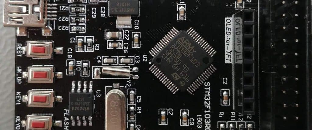
Printed circuit boards (PCBs) are becoming increasingly complex to accommodate higher density components and more sophisticated functionality. A growing trend is the use of boards with a large number of layers – 8, 10, 12 or more. In particular, many advanced designs are moving to 10 layer PCBs.
While providing more real estate for routing complex circuitry, manufacturing quality multilayer PCBs introduces challenges not present with simpler 2 layer or 4 layer designs. Great care must be taken designing the layer stackup and meeting fabrication capabilities to produce a fully functional 10 layer board.
This article provides a comprehensive guide to engineering and manufacturing considerations for high quality 10 layer PCBs. We’ll cover key stackup strategies, layer sequence, material selection and fabrication processes to yield a robust multilayer board.
Benefits of 10 Layer PCBs

Adding more layers provides several advantages that become essential for dense, high speed designs:
- More routing channels – With 10 layers, routing congestion is greatly reduced allowing complex, high pin count ICs.
- High speed design – Proper stackup essential for controlled impedance lines on inner layers.
- Smaller board sizes – More compact layout fitting into smaller enclosures.
- Higher component density – Allows minimum component spacing and footprint size.
- RF/high frequency design – Additional layers help control losses, parasitics and shielding.
- Complex power distribution – Extra layers provide power planes and decoupling capacitors near ICs.
- Mixed signal separation – Digital and analog signals can be isolated on separate layers.
For these reasons, the transition from 4 layer to 6 or more layers is common as PCBs must support more advanced functionality. However, the fabrication process also increases in complexity.
Challenges of High Layer Count PCBs
While offering advantages, moving to a 10 layer PCB also creates difficulties to address:
- Increased cost – Each additional layer adds expense for materials, processing time and lower yields.
- Panelization strategy – Must allow handling of thin multilayer panels with many small boards.
- Registration – Tighter alignment tolerances are needed for high density vias between layers.
- Aspect ratios – High layer count leads to thinner individual layers and higher aspect ratio holes.
- Fabrication limits – Not all shops can produce true 10 layer boards within their capabilities.
- Testing – Requires rigorous testing for potential issues like microvias or lamination voids.
- Rework difficulties – Repairing or modifying multilayer boards is much harder after fabrication.
With careful planning, these challenges can be avoided through robust stackup design, strict manufacturing standards and working with capable fabrication partners.
10 Layer Stackup Design

The sequence of material layers and their functions is key to maximizing routing area and isolating critical signals. Here are some best practices for 10 layer stackup:
Layer Sequence
The table below shows a typical 10 layer buildup sequence. Signal layers are labelled 1-10 while plane layers are labelled GND or PWR:
| Layer | Function |
|---|---|
| 1 | Signal |
| GND | Ground Plane |
| 2 | Signal |
| PWR | Power Plane |
| 3 | Signal |
| 4 | Signal |
| 5 | Signal |
| 6 | Signal |
| PWR | Power Plane |
| 7 | Signal |
| GND | Ground Plane |
| 8 | Signal |
| 9 | Signal |
| 10 | Signal |
- Ground and power plane layers are inserted every 2-3 signal layers to provide decoupling capacitors the shortest distance to ICs.
- High speed signals requiring impedance control are routed on layers 4-7 near the board center to minimize skew and attenuation.
- Layer 10 should be avoided for critical signals since registration capability often decreases for outer layers.
Dielectric Materials
Common PCB laminates like FR-4 can be used for 10 layer boards. Some considerations:
- Standard 1.6 mm FR-4 thickness is difficult beyond 6-8 layers. Thinner laminates of 0.8-1.2mm are preferable.
- Low Dk glass reinforced materials are better for higher frequencies compared to standard FR-4.
- Tg (glass transition temperature) should be >170°C for lead-free soldering and high reliability.
- Tight weave glass styles minimize resin pocket depth for maximum dielectric consistency.
Copper Thickness
Ultra-thin copper foils down to 1⁄4 oz (7 μm) may be needed on inner layers to achieve fine trace/space. However, thicker copper is desirable for current carrying layers:
| Location | Copper Thickness |
|---|---|
| High current power layers | 2 oz (70 μm) |
| Outer layers | 1 oz (35 μm) |
| Signal Layers | 1⁄2-1 oz (17-35 μm) |
Mask Defined Pads
Solder mask defined land patterns are preferable for higher density component pads which improve registration tolerance. The solder mask layer defines the pad geometry rather than the copper layer.
Impedance Control
Controlled impedance lines require very tight stackup tolerances. Coordinate with your PCB fabricator on required stackup accuracy. 10 layers provides multiple possible configurations for matched Z0.
Following these guidelines will maximize the routability and performance of a 10 layer PCB while meeting fabrication capabilities.
10 Layer PCB Fabrication

Achieving a high quality 10 layer board requires advanced fabrication processes. Here are key considerations during manufacturing:
Layer Registration
Typical registration between layers is around 75-100 μm for lower layer counts. However, 10 layers may require 50 μm or tighter registration, involving precision drilling and careful layer alignment during lamination.
Hole Wall Quality
With over 30 drilled holes required for connectivity through all 10 layers, excellent hole wall copper and resin coverage is mandatory. Semi-additive or high throwing power electroless processes produce the most reliable via connections.
Thin Core Requirements
Most 10 layer boards will utilize thinner dielectric cores compared to typical 1.6mm. Panel yields decrease as core thickness drops below 0.8mm, so frame design and handling becomes critical.
Oxide Alternative Processes
Oxide alternative chemistries produce finer line resolution compared to traditional subtractive etch when working with ultra-thin inner layer copper foils. This avoids over-etching during multilayer inner layer patterning.
Test Coupons
Inclusion of microsection coupons on panels allows evaluating layer quality and registration under a microscope during fabrication. These can catch potential issues like resin voids before completing the multilayer build.
Electrical Test
Testing for potential shorts between traces requires flying probe testers or fixtures to access inner conductors. IST or boundary scan testing can also verify interconnect reliability of hidden vias.
Panel Design
Frame and panel layout must provide adequate tooling holes for registration while minimizing stress on thinner multilayer boards during depanelization. Large panels with many small boards require subdivision into smaller panels.
By partnering with a high density PCB manufacturer experienced in true 10+ layer boards, potential pitfalls can be avoided to produce a reliable, functional multilayer PCB. Expect higher costs but maximize value through optimized stackup design.
Thermal Management
The insulation property of FR-4 laminate materials leads to thermal challenges when sandwiching many conductive copper layers. Here are some ways to mitigate excessive thermal rise in multilayer PCBs:
- Incorporate thermally conductive dielectric materials like aluminum oxide or boron nitride filled polymers.
- Allow adequate airflow and heat sinking on outer surfaces where components dissipate significant thermal energy.
- Use multiple smaller vias in parallel to conduct heat between layers. Copper fills inside blocking air pockets in holes.
- Consider thermal vias under hot components connecting directly to backside metal heat sinking features.
- Specify laminates with higher thermal conductivity if high power components are used.
- Model the thermal performance early in design process using thermal simulation and finite element analysis tools.
With careful engineering, even high power dissipating 10 layer boards can be effectively cooled.
Design for Manufacturing
Here are some 10 layer board guidelines to maximize manufacturing yield and minimize cost:
- Allow 5-10X spacing around panel edges for tooling and clamping pressure.
- Follow minimum annular ring, hole size, and trace spacing rules provided by your fabricator.
- Use least number of different hole sizes. All holes below 0.15mm require advanced drilling equipment.
- Minimize use of blind and buried vias to reduce process steps. Through hole vias are most reliable.
- Maintain symmetry from board centerline whenever possible as registration decreases on outer layers.
- Allow test points access to internal layers for validation of all nets.
Early engagement with your PCB production partner can inform design choices and avoid problematic features.
Conclusion
Migrating to a 10 layer PCB stackup enables increased routing density, integrated shielding, impedance control, and power distribution needed for cutting edge electronics. However, fabricating quality multilayer boards requires careful stackup planning and advanced manufacturing capabilities.
By applying the guidelines in this article around stackup sequence, material selection, hole registration, panelization and thermal management, engineers can fully utilize 10 or more layers for their complex designs. Partnering with a shop experienced in high layer count boards ensures achieving the quality and functionality required to maximize your product’s capabilities and service life.
Frequently Asked Questions

What are the most common layer counts beyond 6 layer PCBs?
The most common complex PCBs are typically 8, 10, or 12 total layers. Component density and routing channels generally drive the need for more layers. High frequency designs may use additional layers for shielding.
What is a typical dielectric thickness for a 10 layer board?
Because of the total thickness constraints, 10 layer boards typically use thinner dielectric cores in the range of 0.8mm to 1.2mm, compared to 1.6mm commonly used in simpler 4 layer boards. This maintains a reasonable overall thickness.
What are the disadvantages of using thin laminate materials?
Thinner laminate cores decrease panel rigidity, making handling more difficult and lowering fabrication yield. Registration and line resolution also decrease on more flexible boards. Some exotic materials are limited in thin core availability.
Why is symmetry important in 10 layer PCB stackups?
A symmetric sequence of dielectric materials and copper layers minimizes warpage and internal stresses. Thermal expansion differences can cause bowing or delamination with an asymmetric construction.
What special considerations are needed for buried and blind vias?
Buried and blind vias require additional processing steps and yield loss over standard through hole vias. The layer transitions must also be carefully modeled for impedance control. Tighter registration capability is needed.