The X-ray inspection is part of the process control in our quality management system, Not only detect issues in SMT, but the analysis of an X-Ray image can help to determine the root cause of a given defect, such as insufficient solder paste, skewed part placement, or improper reflow soldering profile.
To guarantee the optimal performance of electronic devices, X-ray inspection is conducted on PCBs at every stage of the assembly process. Since various categories of circuit boards adhere to different inspection standards, X-ray inspection has become a widely utilized technique. It is particularly effective in identifying defects that are invisible to the naked eye, ensuring higher quality and reliability.
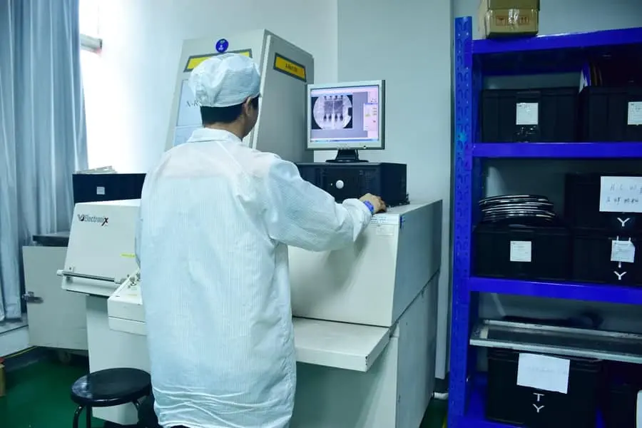
PCB X-Ray Inspection is a non-destructive testing method that uses X-ray technology to examine the internal structures of printed circuit boards. This advanced technique allows manufacturers to peer inside complex PCBs without causing any damage, revealing hidden defects that might otherwise go unnoticed until product failure.
While traditional inspection methods like optical and visual inspections are still valuable, they’re limited to surface-level examinations. PCB X-Ray Inspection takes quality control to the next level by providing:
As PCBs evolve to accommodate more complex designs, X-ray inspection becomes increasingly vital. It’s particularly crucial for:
These advanced PCBs often have hidden solder joints, internal vias, and densely packed components that are impossible to inspect visually, making X-ray technology an essential quality assurance tool.

At its core, PCB X-Ray Inspection relies on the same principles that make medical X-rays possible. Here’s a simplified breakdown of the process:
PCB X-Ray Inspection comes in several flavors, each with its own strengths:
2D X-ray Inspection:
2.5D X-ray Inspection:
3D CT (Computed Tomography) Inspection:

Implementing PCB X-Ray Inspection in the manufacturing process brings a host of advantages that contribute to higher quality products and more efficient operations.
X-ray inspection excels at uncovering issues that would otherwise remain invisible until product failure. These include:
As PCBs become more intricate, traditional inspection methods fall short. X-ray inspection provides:
By catching defects early, X-ray inspection helps:
While X-ray inspection systems represent an investment, they often pay for themselves by:
X-ray inspection is particularly adept at identifying several types of PCB defects that can compromise performance and reliability.
Voids are small air pockets or gaps within solder joints. While some level of voiding is often acceptable, excessive voids can lead to:
X-ray inspection can quantify the percentage of voiding in each joint, allowing manufacturers to ensure they meet industry standards.
Open circuits occur when there’s a break in the electrical path. X-ray inspection can reveal:
These issues might not be visible from the surface but can cause intermittent or complete failure of the PCB.
Short circuits happen when there’s an unintended connection between two points in a circuit. X-ray inspection helps identify:
Catching these defects early prevents potentially catastrophic failures down the line.
Proper component placement is crucial for PCB functionality. X-ray inspection can detect:
These alignment issues can cause intermittent connections or complete component failure.
For multilayer PCBs, X-ray inspection is invaluable in identifying defects within the board itself:
Such internal defects are impossible to spot with visual inspection alone and can lead to long-term reliability issues if left unchecked.

The versatility and effectiveness of PCB X-Ray Inspection make it an invaluable tool across various sectors where electronic reliability is paramount.
In an industry where failure is not an option, X-ray inspection ensures:
As vehicles become increasingly reliant on electronics, X-ray inspection helps:
In the competitive world of consumer devices, X-ray inspection contributes to:
For medical equipment where lives are at stake, X-ray inspection provides:
In the realm of global connectivity, X-ray inspection ensures:

While PCB X-Ray Inspection offers numerous benefits, it’s important to be aware of its limitations to use the technology effectively.
Selecting a PCB X-Ray Inspection provider is a crucial decision that can significantly impact your product quality and manufacturing efficiency.
Machine Capabilities:
Expertise and Experience:
Turnaround Time:
Reporting and Analysis:
Customer Support:

The field of PCB X-Ray Inspection continues to evolve, with several exciting developments on the horizon.
At RayPCB, we understand the critical role that X-ray inspection plays in ensuring the quality and reliability of your PCBs. Our state-of-the-art X-ray inspection capabilities are just one part of our comprehensive PCB manufacturing and quality assurance services.
Our clients across various industries have benefited from our meticulous X-ray inspection services:
Ready to experience the RayPCB difference? Contact us today for a quote or to discuss how our X-ray inspection services can enhance your PCB quality assurance process.
PCB X-Ray Inspection has become an indispensable tool in the quest for electronic perfection. As we’ve explored, its ability to peer into the hidden layers of PCBs provides unparalleled insight into potential defects and quality issues. From ensuring the reliability of life-saving medical devices to guaranteeing the performance of your smartphone, X-ray inspection plays a crucial role in our increasingly electronic world.
By embracing this technology, manufacturers can:
As PCBs continue to evolve, becoming more complex and miniaturized, the importance of X-ray inspection will only grow. Forward-thinking companies are already integrating this technology into their quality assurance processes, reaping the benefits of improved yields, enhanced reliability, and stronger customer trust.
Don’t let hidden defects compromise your products’ integrity. Partner with RayPCB to leverage our cutting-edge X-ray inspection capabilities and ensure that your PCBs meet the highest standards of quality. Contact us today to learn how we can support your commitment to excellence in electronics manufacturing.
Q: How long does a typical PCB X-ray inspection take? A: The duration can vary depending on the complexity of the PCB and the type of inspection (2D, 2.5D, or 3D CT). A simple 2D scan might take just a few minutes, while a comprehensive 3D CT scan could take several hours.
Q: Is X-ray inspection safe for the PCB components? A: Yes, PCB X-ray inspection is non-destructive and does not harm the electronic components or the board itself when performed correctly.
Q: Can X-ray inspection detect all types of PCB defects? A: While X-ray inspection is highly effective, it’s not infallible. Some surface-level defects might be better detected by optical inspection. It’s often best to use X-ray inspection as part of a comprehensive quality control strategy.
Q: How often should PCBs be X-ray inspected during production? A: This depends on your quality control needs and production volume. Some manufacturers inspect every board, while others use statistical sampling. Critical applications often require 100% inspection.
Q: What’s the difference between X-ray inspection and CT scanning for PCBs? A: X-ray inspection typically refers to 2D or 2.5D imaging, while CT (Computed Tomography) scanning creates a full 3D model of the PCB’s internal structure, allowing for virtual “slicing” of the board in any plane.