Today’s electronics demand increasingly compact, high-speed PCB designs where every trace and component interaction matters. As operating frequencies routinely reach GHz ranges and signal integrity becomes paramount, simple conductor connections no longer suffice.
Controlled impedance has emerged as a critical factor in PCB performance. Designers must now carefully analyze critical nets, trace geometries, and their board’s material properties to maintain signal quality. In high-speed digital and RF applications, proper impedance management isn’t just beneficial – it’s essential for reliable circuit operation.
What is Impedance Control PCB?
Impedance control PCB refers to the process of designing and manufacturing printed circuit boards with specific trace impedances. This technique ensures that the electrical characteristics of PCB traces remain consistent throughout the signal path, which is critical for maintaining signal integrity in high-speed and high-frequency applications.
Why is Impedance Control Important in PCB Design?
Impedance control PCB design is crucial for several reasons:
- Signal Integrity: It minimizes signal reflections and distortions, ensuring clean signal transmission.
- High-Speed Performance: Essential for devices operating at high frequencies or data rates.
- Electromagnetic Compatibility (EMC): Helps reduce electromagnetic interference (EMI) and improve overall system performance.
- Compliance: Many industry standards require specific impedance values for certain interfaces.
Types of Controlled Impedance in PCBs
When discussing impedance control PCB design, it’s important to understand the different types of controlled impedance configurations:
Single-Ended Impedance
Single-ended impedance is the most common type in impedance control PCB design. It refers to the impedance of a single trace measured against a reference plane (usually ground). Typical values for single-ended impedance are 50Ω or 75Ω, depending on the application.
Differential Impedance
Differential impedance involves a pair of traces carrying complementary signals. The impedance is measured between these two traces. Differential pairs are commonly used in high-speed digital interfaces like USB, HDMI, and PCIe. Typical differential impedance values are 100Ω or 120Ω.
Coplanar Impedance
Coplanar impedance refers to traces on the same layer with ground planes on either side. This configuration is often used in RF and microwave circuits. The impedance in coplanar waveguides depends on the trace width, the gap between the trace and adjacent ground planes, and the dielectric properties of the substrate.
Lear more about:
Factors Affecting Impedance Control PCB Design
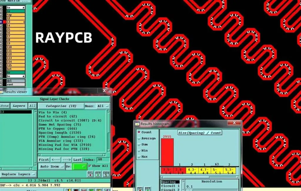
Several factors influence the impedance of PCB traces. Understanding these factors is crucial for effective impedance control PCB design:
1. Trace Geometry
The width and thickness of the trace significantly affect its impedance. Wider traces generally have lower impedance, while narrower traces have higher impedance.
2. Dielectric Material
The properties of the dielectric material, particularly its relative permittivity (εr), play a crucial role in determining trace impedance.
3. Stackup Design
The arrangement of layers in the PCB, including the distance between signal layers and reference planes, impacts impedance.
4. Copper Weight
The thickness of the copper used for traces (often referred to as copper weight) affects both the trace’s resistance and its impedance.
5. Surface Finish
Different surface finishes can slightly alter the effective dimensions of the traces, impacting their impedance.

How to Calculate Impedance in PCB Design
Calculating impedance is a critical step in impedance control PCB design. While sophisticated software tools are available for precise calculations, understanding the basic formulas provides valuable insights:
Microstrip Impedance Calculation
For a microstrip (a trace on the outer layer with a ground plane beneath), the impedance can be approximated using:
Z0 = [87 / (√(εr + 1.41))] * ln(5.98h / (0.8w + t))
Where:
- Z0 is the characteristic impedance
- εr is the relative permittivity of the substrate
- h is the height of the trace above the ground plane
- w is the width of the trace
- t is the thickness of the trace
Stripline Impedance Calculation
For a stripline (a trace embedded between two ground planes), the impedance can be approximated using:
Z0 = [60 / √εr] * ln[1.9b / (0.8w + t)]
Where:
- b is the distance between the ground planes
- Other variables are the same as in the microstrip formula
It’s important to note that these formulas are approximations. For precise impedance control PCB design, especially in high-speed or RF applications, it’s recommended to use specialized PCB design software or consult with PCB manufacturers.
Best Practices for Impedance Control PCB Design
Implementing effective impedance control PCB design requires attention to detail and adherence to best practices:
1. Maintain Consistent Trace Width
Keep trace widths consistent throughout the signal path to maintain uniform impedance.
2. Use Smooth Transitions
Avoid abrupt changes in trace direction. Use curved traces or 45-degree angles for turns.
3. Proper Stackup Design
Design your PCB stackup carefully, ensuring consistent reference planes for controlled impedance traces.
4. Mind the Return Path
Ensure a clear and uninterrupted return path for high-speed signals, typically on an adjacent layer.
5. Differential Pair Routing
For differential pairs, maintain tight coupling and equal length between the two traces.
6. Avoid Impedance Discontinuities
Minimize the use of vias in controlled impedance traces, as they can introduce impedance discontinuities.
7. Use Stitching Vias
When changing layers, use stitching vias near the transition to maintain a consistent return path.
Manufacturing Considerations for Impedance Control PCB
Successful impedance control PCB manufacturing requires close collaboration between designers and manufacturers. Here are key considerations:
1. Material Selection
Choose appropriate PCB materials with consistent dielectric properties for reliable impedance control.
2. Copper Weight
Specify the correct copper weight, as it affects both trace impedance and manufacturability.
3. Tolerances
Understand and specify the required tolerances for trace width and spacing, as well as overall board thickness.
4. Testing and Verification
Implement proper testing procedures, such as Time Domain Reflectometry (TDR), to verify impedance values.
5. Documentation
Provide clear and detailed documentation of impedance requirements to your PCB manufacturer.
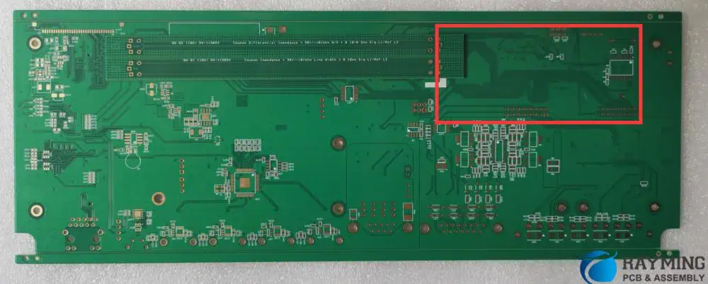
Measuring Impedance in Manufactured PCBs

Verifying the impedance of manufactured PCBs is crucial for quality control. Here are common methods for measuring impedance:
1. Time Domain Reflectometry (TDR)
TDR is the most common method for measuring PCB trace impedance. It sends a fast rise-time pulse down the trace and measures reflections caused by impedance discontinuities.
2. Vector Network Analyzer (VNA)
VNAs are powerful tools for measuring impedance, especially useful for RF and microwave circuits. They measure scattering parameters (S-parameters) of the trace, which can be used to calculate impedance.
3. Impedance Coupon Testing
Many PCB manufacturers offer impedance coupon testing as part of their quality control process. Test coupons with controlled impedance traces are included on the panel with the PCBs and measured using TDR or other methods.
Advanced Topics in Impedance Control PCB Design
As you delve deeper into impedance control PCB design, consider these advanced topics:
1. High-Speed Design Considerations
For high-speed designs, factors like skin effect and dielectric loss become increasingly important. These phenomena can affect signal integrity and must be accounted for in impedance calculations and overall PCB design.
2. Impedance Control in Flexible PCBs
Flexible and rigid-flex PCBs present unique challenges for impedance control. The bending of traces and varying dielectric properties in different areas of the board require special consideration.
3. Electromagnetic Simulation
Advanced electromagnetic simulation tools can provide detailed insights into signal behavior and impedance characteristics, allowing for more precise impedance control PCB design.
4. Embedded Passives and Impedance Control
The use of embedded passive components can impact impedance control. Understanding how to design and manufacture PCBs with embedded passives while maintaining controlled impedance is an advanced skill.
Troubleshooting Common Impedance Control PCB Issues
Even with careful design and manufacturing, impedance control PCB issues can arise. Here are some common problems and their solutions:
1. Impedance Mismatch
Symptom: Signal reflections and degraded signal quality. Solution: Verify trace widths, dielectric thicknesses, and material properties. Adjust design or manufacturing process as needed.
2. Crosstalk
Symptom: Interference between adjacent traces. Solution: Increase spacing between traces, use guard traces, or adjust layer stackup to improve isolation.
3. Inconsistent Impedance Along Trace Length
Symptom: Varying signal quality at different points along the trace. Solution: Ensure consistent trace width and reference plane integrity throughout the signal path.
4. Resonance Issues
Symptom: Signal integrity problems at specific frequencies. Solution: Analyze and adjust trace lengths to avoid creating unintentional resonant structures.
Future Trends in Impedance Control PCB Design
As technology continues to advance, impedance control PCB design is evolving to meet new challenges:
1. Higher Frequencies
With the advent of 5G and beyond, PCB designs must accommodate ever-higher frequencies, requiring more precise impedance control.
2. Miniaturization
As devices become smaller, maintaining controlled impedance in dense, compact layouts becomes more challenging.
3. New Materials
Development of new PCB materials with improved dielectric properties will offer new possibilities for impedance control in high-performance applications.
4. Artificial Intelligence in PCB Design
AI-assisted design tools are emerging, potentially revolutionizing how we approach impedance control PCB design and optimization.
Conclusion
Mastering impedance control PCB design is essential for creating high-performance electronic products in today’s fast-paced technological landscape. From understanding the basic principles to implementing advanced techniques, this guide has covered the critical aspects of controlled impedance in PCB design and manufacturing.
Remember, successful impedance control PCB design is not just about following rules and formulas. It requires a deep understanding of electromagnetic principles, close collaboration between designers and manufacturers, and a commitment to continuous learning and improvement.
As you apply these principles in your PCB projects, you’ll develop an intuition for impedance control that goes beyond mere calculations, leading to more robust and reliable electronic products. Whether you’re designing high-speed digital circuits, sensitive analog systems, or cutting-edge RF applications, mastering impedance control PCB design is an essential skill that will set your work apart in the ever-evolving field of electronics.