In the ever-evolving world of electronics, the demand for faster and more efficient devices continues to grow. As signal speeds increase, maintaining signal integrity becomes a critical challenge for PCB designers. One technique that has emerged as a powerful solution is back drilling. This article will delve into the intricacies of back drilling in PCB manufacturing, exploring its benefits, processes, and applications in high-speed designs.
What is a Backdrill Via?
Before we dive into the specifics of back drilling, it’s essential to understand what a backdrill via is and why it’s crucial in PCB design.
Definition of a Backdrill Via
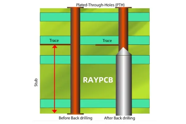
A backdrill via, also known as a controlled depth via, is a plated through-hole (PTH) in a printed circuit board that has been partially drilled out from one or both sides. This process removes the unused portion of the via barrel, leaving only the necessary interconnection between layers.
The Need for Backdrilled Vias
In high-speed PCB designs, traditional plated through-holes can act as stubs, causing signal reflections and degrading signal integrity. Backdrilled vias address this issue by eliminating these stubs, thereby improving signal quality and allowing for higher data rates.
How Back Drilling Works in PCB

Understanding the process of back drilling is crucial for both PCB designers and manufacturers. Let’s break down the steps involved in this precision technique.
The Back Drilling Process
- Initial Via Creation: The process begins with a standard plated through-hole via.
- Depth Calculation: Engineers determine the optimal depth for back drilling based on the required layer connections.
- Precision Drilling: Using specialized equipment, the unused portion of the via is carefully drilled out.
- Depth Control: Advanced machinery ensures that the drilling stops at the precise depth, leaving the necessary connections intact.
Key Considerations in Back Drilling
- Drill Bit Selection: The choice of drill bit is crucial for achieving the required precision.
- Depth Accuracy: Maintaining consistent depth across all backdrilled vias is essential for optimal performance.
- Board Material: The PCB material can affect the back drilling process and must be considered in the design phase.
Advantages of Back Drilling PTH Vias
Back drilling offers several significant benefits for high-speed PCB designs. Let’s explore these advantages in detail.
Improved Signal Integrity
- Reduced Signal Reflections: By removing unused via stubs, back drilling minimizes signal reflections that can cause distortion.
- Enhanced Signal Quality: The cleaner signal path results in improved overall signal quality and reduced noise.
Increased Bandwidth
- Higher Data Rates: Back drilling allows for higher frequency signals to be transmitted without degradation.
- Extended Reach: It enables longer trace lengths for high-speed signals, expanding design possibilities.
Design Flexibility
- Layer Stack-up Options: Back drilling provides more flexibility in layer stack-up design, allowing for optimized signal routing.
- Component Placement: It can free up board space, offering more options for component placement.
Cost-Effectiveness
- Alternative to Microvias: In some cases, back drilling can be a more cost-effective solution compared to using microvias.
- Improved Yield: By enhancing signal integrity, back drilling can lead to higher manufacturing yields and reduced rework costs.
Read more about:
Controlled Depth Drilling from a Design Perspective (By Altium Designer)
Altium Designer, a popular PCB design software, offers robust features for implementing back drilling in your designs. Let’s walk through the process step by step.
1. Selecting the Circuit Segment
- Open your PCB design in Altium Designer.
- Identify the high-speed circuit segments that would benefit from back drilling.
2. Adding a Back Drill Via
- Navigate to the PCB editor.
- Select the via you wish to back drill.
- Right-click and choose “Properties”.
- In the via properties dialog, enable the “Back Drill” option.
3. Selecting the Start and Stop Layer
- In the via properties, specify the start and stop layers for back drilling.
- Ensure that the remaining via length connects the necessary layers.
4. Adding a Design Rule
- Go to “Design” > “Rules”.
- Create a new Back Drill rule.
- Define the scope and constraints for back drilling.
5. Checking the Back Drills
- Use the “Design Rule Check” (DRC) feature to verify your back drill settings.
- Resolve any issues highlighted by the DRC.
6. Viewing Backdrilling PCB Drill Table
- Generate a drill table report.
- Review the back drill information, including depths and affected vias.
7. Backdrilling in PCB Manufacturing
- Ensure that your design output includes clear back drilling instructions for the manufacturer.
- Consider adding notes or a separate document detailing back drill requirements.
8. Backdrilling PCB DFM Tip
- Consult with your PCB manufacturer early in the design process.
- Understand their back drilling capabilities and limitations to optimize your design.
How Back Drilling Improves Via Signal Integrity in High-Speed PCBs
Back drilling plays a crucial role in enhancing signal integrity, particularly in high-speed PCB designs. Let’s delve into the specifics of how this technique achieves these improvements.
Elimination of Via Stubs
- Stub Effect: In traditional PTH vias, the unused portion acts as a stub, causing signal reflections.
- Stub Removal: Back drilling eliminates these stubs, creating a cleaner signal path.
Reduced Signal Reflections
- Impedance Discontinuities: Via stubs create impedance discontinuities that lead to signal reflections.
- Smoother Transitions: By removing stubs, back drilling ensures smoother impedance transitions along the signal path.
Minimized Crosstalk
- Coupling Reduction: Shorter via barrels reduce coupling between adjacent signals.
- Improved Isolation: This leads to reduced crosstalk and better signal isolation.
Enhanced Bandwidth
- Frequency Response: Back drilled vias have a better frequency response compared to standard PTH vias.
- Higher Data Rates: This allows for higher data rates and improved overall system performance.
The Manufacturing Process of Back Drilling

Understanding the manufacturing process of back drilling is crucial for both designers and manufacturers. Let’s break down the key steps and considerations.
Pre-Production Planning
- Design Review: Carefully review the PCB design to identify all vias requiring back drilling.
- Tooling Preparation: Select appropriate drill bits and set up the back drilling equipment.
Drilling Process
- Board Alignment: Precisely align the PCB on the drilling machine.
- Depth Calibration: Calibrate the drilling depth for each via based on design specifications.
- Controlled Drilling: Execute the back drilling process, carefully controlling depth and speed.
- Inspection: Conduct real-time inspection to ensure drilling accuracy.
Post-Drilling Procedures
- Cleaning: Remove any debris generated during the drilling process.
- Quality Control: Perform thorough checks to verify drilling depth and quality.
- Measurement and Verification: Use precision measurement tools to confirm back drill depths.
Challenges and Considerations
- Drill Bit Wear: Monitor and replace drill bits regularly to maintain precision.
- Material Considerations: Adjust drilling parameters based on PCB material properties.
- Thermal Management: Manage heat generation during drilling to prevent board damage.
The Application of Back Drilled Vias
Back drilling finds applications in various high-speed and high-frequency PCB designs. Let’s explore some key areas where this technique proves invaluable.
Telecommunications Equipment
- High-Speed Routers: Back drilling enables cleaner signal transmission in complex routing systems.
- 5G Infrastructure: Essential for maintaining signal integrity in high-frequency 5G equipment.
Data Centers
- Server Boards: Back drilling allows for higher data rates in densely packed server environments.
- Storage Systems: Improves reliability in high-speed data storage applications.
Aerospace and Defense
- Radar Systems: Enhances signal quality in sensitive radar equipment.
- Avionics: Ensures reliable communication in critical aerospace applications.
Automotive Electronics
- Advanced Driver Assistance Systems (ADAS): Supports high-speed data processing in modern vehicles.
- Infotainment Systems: Enables faster, more reliable in-car entertainment and information systems.
Test and Measurement Equipment
- Oscilloscopes: Improves accuracy in high-frequency measurement devices.
- Signal Generators: Enhances signal quality in precision testing equipment.
Consumer Electronics
- High-End Smartphones: Supports faster data transfer and processing in premium mobile devices.
- Gaming Consoles: Enables smoother, high-speed graphics processing and data handling.
Conclusion: The Future of Back Drilling in PCB Design
As we’ve explored throughout this article, back drilling has become an indispensable technique in high-speed PCB design. Its ability to enhance signal integrity, increase bandwidth, and provide design flexibility makes it a powerful tool in the PCB designer’s arsenal.
Emerging Trends
- Automation: Increasing automation in back drilling processes for improved precision and efficiency.
- Advanced Materials: Development of new PCB materials optimized for back drilling applications.
- Integration with Design Software: Closer integration of back drilling considerations in PCB design software.
Challenges and Opportunities
- Cost Optimization: Balancing the benefits of back drilling with manufacturing costs.
- Education and Training: Ensuring PCB designers are well-versed in back drilling techniques and best practices.
- Standards Development: Establishing industry-wide standards for back drilling processes and quality control.
As the demand for faster, more efficient electronic devices continues to grow, the importance of techniques like back drilling will only increase. By understanding and leveraging this technology, PCB designers and manufacturers can stay at the forefront of high-speed electronic design, delivering products that meet the ever-increasing demands of modern technology.
In conclusion, back drilling in PCB manufacturing represents a critical advancement in high-speed design. As we’ve seen, it offers significant improvements in signal integrity, bandwidth, and design flexibility. For engineers and manufacturers working on cutting-edge electronic products, mastering the art and science of back drilling is not just beneficial—it’s essential for staying competitive in today’s fast-paced technological landscape.