PCB Manufacturing

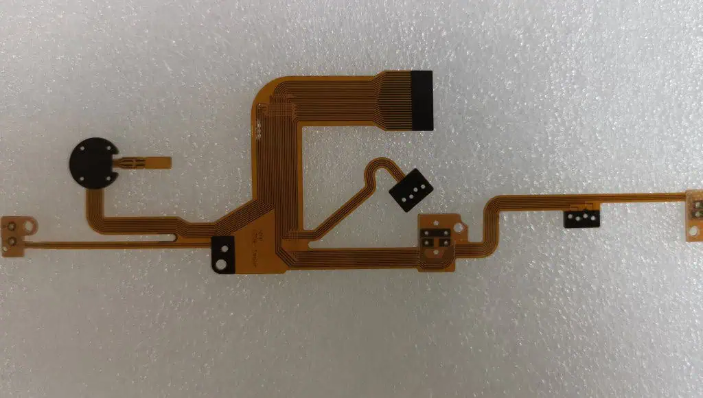
Advanced PCB manufacturing services, specializing in high-precision, high-difficulty, and special materials, serving industries such as scientific research, aviation, military, medical, robotics, and AI.

About Us

20 Years PCB Manufacturer

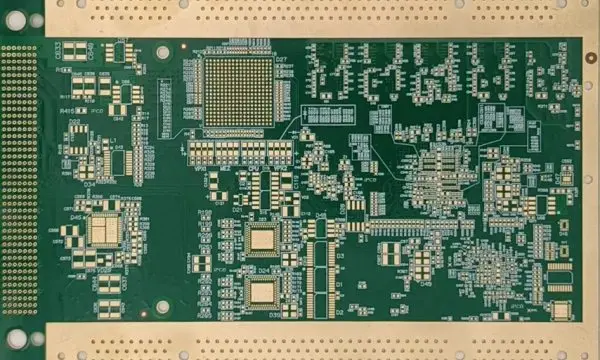
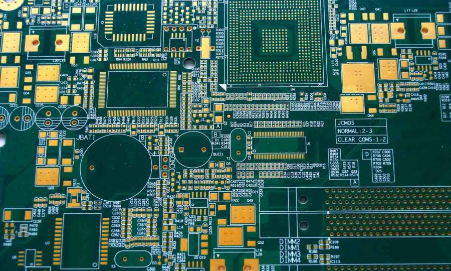
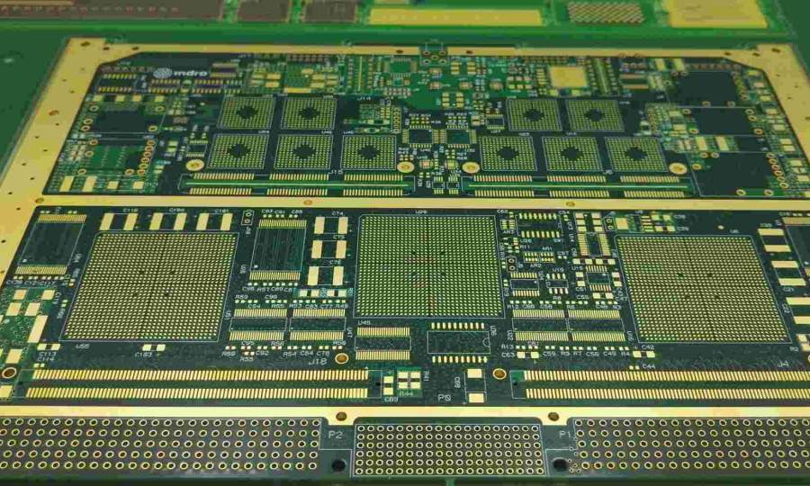
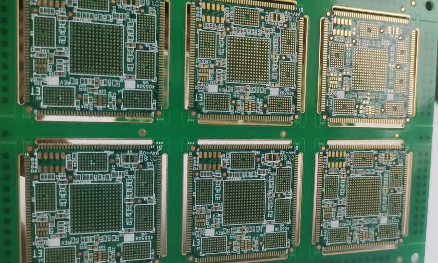
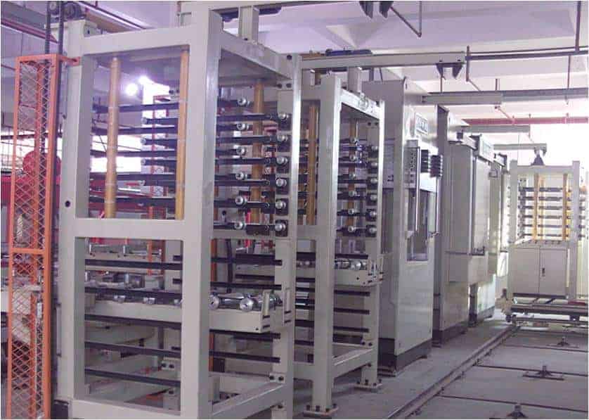
RAYMING PCB is a leading provider of cutting-edge printed circuit board manufacturing technologies, delivering the highest quality standards for the electronics industry. Our unwavering commitment to technological leadership drives us to continuously innovate and meet new design challenges.

Our state-of-the-art innovation lab and expert engineering team specialize in overcoming complex design hurdles, including:

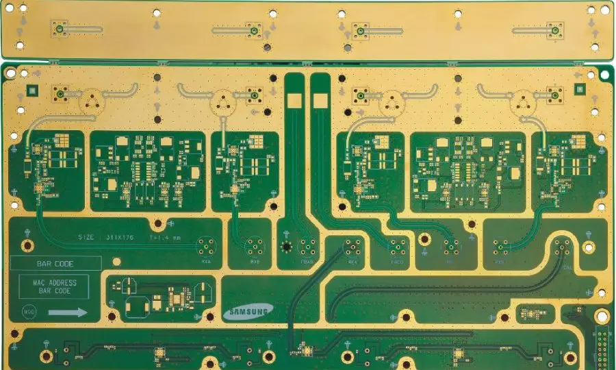
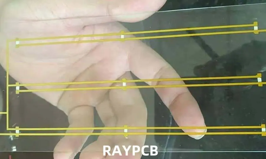
  1. High Speed and High Capacity circuits
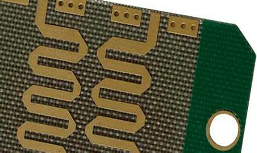
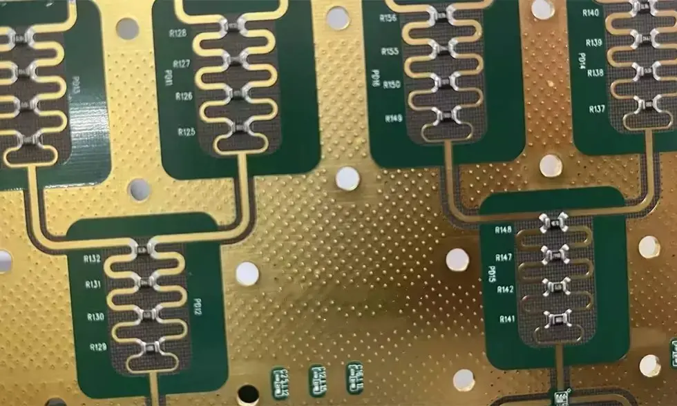
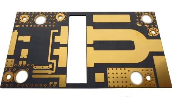
  2. RF and Microwave technology
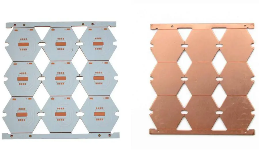
  3. Thermal Management solutions
  4. Miniaturization techniques
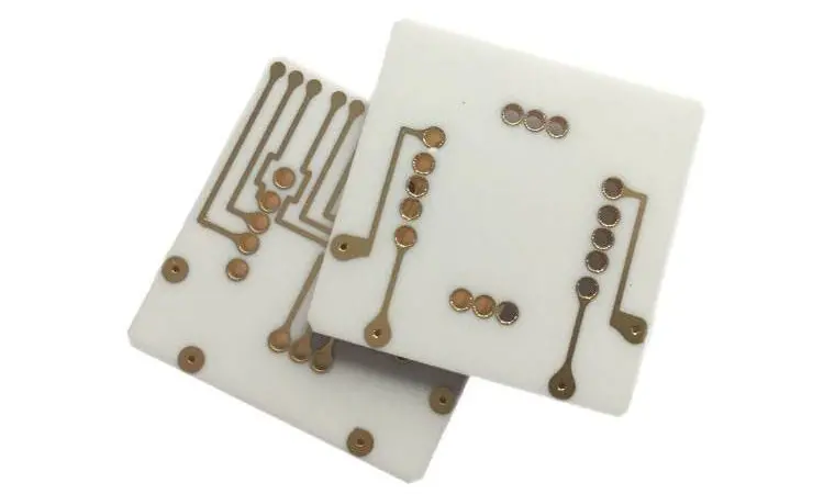
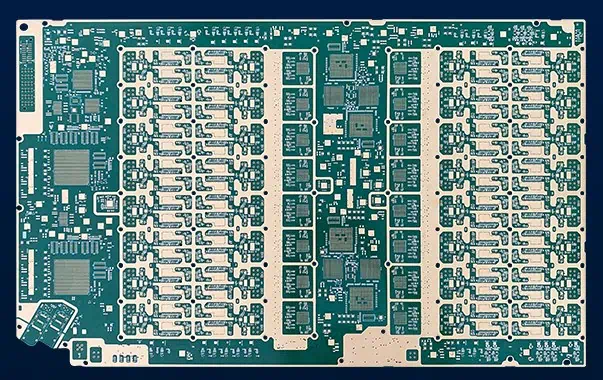
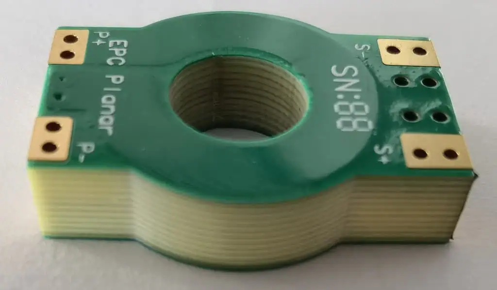
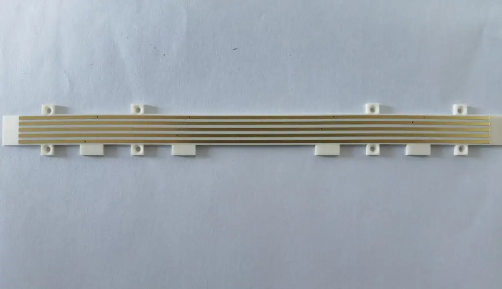
  5. Chip package substrates

We offer tailored solutions for various industries, including 5G, AI Robotics, and Battery Management Systems (BMS). Our technical capabilities encompass:

RAYMING welcomes complex RFQs for cost estimation. We are proud to hold UL Certifications for our products:

  • Rigid PCB/Aluminum PCB: E472163
  • Flex PCB/Rigid-flex PCB: E544606

Latest PCB Projects

5G TRX PCB

optical module PCB

Medical PCB

Rogers 4350B + Copper Base PCB

Hybrid PCB: Rogers 4350B + Copper Base PCB

32 layer PCB

32 Layer PCB Manufacturing with 6.5mm thickness, Motor EPC Application

Ceramic PCB

Ceramic PCB manufacturing with Step holes + bevelled edges process

Radar RF PCB

8 Layer 77 GHz millimeter wave radar, Material: Ro3000+IT180A

14 layer SSD PCB

14 Layer High TG FR4+ PI, 4 Step HDI PCB

E-band ODU RF Board

4 Layer 1oz E-band ODU RO4350+FR4 Hybrid PCB

Flexible PCB

2 Layer Flex PCB with PI & FR4 stiffener

Rogers 4350b pcb

Rogers 4350B PCB manufacturing, 0.8mm thickness

PCB Manufacturing Capability

emsMassPrototypes
Layers1-18 Layers PCB1-56 Layers PCB
Max. Panel Size600*770mm( 23.62″*30.31″)600*770mm(23.62″*30.31″) 500*1200mm(19.69″*47.24″)
Max.Board Thickness8.5mm8.5mm
Min. Board Thickness2L:0.3mm2L:0.1mm
4L:0.4mm4L:0.3mm
6L:0.8mm6L:0.6mm
Min Inner Layer Clearance3mil3mil
Min Line width3/3 mil3/3 mil
Min Line space3/3 mil3/3 mil
Min.Hole Size0.1mm0.1mm
Min plated hole thickness25um25um
Min Blind/Buried hole size0.1mm0.1mm(1-18layers)
PTH Dia. Tolerance±0.076mm(±3mil)±0.076mm(±3mil)
Non PTH Dia. Tolerance±0.05mm(±2mil)±0.05mm(±2mil)
Hole Position Deviation±0.05mm(±2mil)±0.05mm(±2mil)
Heavy Coppe4OZ/140μm6OZ/175μm
Min S/M Pitch0.1mm (4mil)0.1mm (4mil)
Soldermask colourGreen,black,Blue,White,Yellow,RedGreen,black,Blue,White,Yellow,Red
Silkscreen colourWhite,Yellow,Red,BlackWhite,Yellow,Red,Black
OutlineRouting,V-Groove, Beveling punchRouting,V-Groove, Beveling punch
Outline Tolerance±0.15mm ±6mil±0.15mm (±6mil)
Peelable maskTop,bottom,double sidedTop,bottom,double sided
Controlled Impedance+/- 10%+/- 7%
Insulation Resistance1×1012Ω(Normal)1×10¹²Ω(Normal)
Through Hole Resistance<300Ω(Normal)<300Ω(Normal)
Thermal Shock3×10sec@288℃3×10sec@288℃
Warp and Twist≤0.7%≤0.7%
Electric Strength>1.3KV/mm>1.4KV/mm
Peel Strength1.4N/mm1.4N/mm
Solder Mask Abrasion>6H>6H
Flammability94V-094V-0
Test Voltage50-330V50-330V