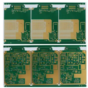
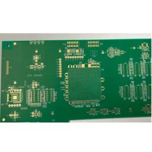
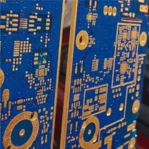
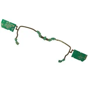
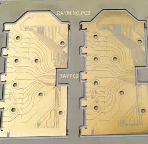
RayMing believes in making your PCB board perfect happen by providing you with quality service and the best FQC inspection. We are proud to stand by our manufacturing management, we are also proud to boast about our high ratio of repeat and loyal customers. When your customers stay with you, you know you”re doing things right.
Because we make no compromises on our incoming quality assurance, we refuse to compromise on our outgoing quality. Our professional team maintain constant vigilance over our processes, we know that our products are created with the best possible processes, and that everything we do conforms to the ISO bodies to which we subscribe.We invite you to rely on our service. We value the faith and trust of our customers above everything, and do everything possible to ensure that your expectations are met or exceeded. We have a proven track record of quality that we intend to maintain.
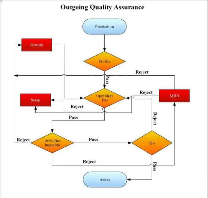
Quality Control Process
1. PCB File Verification Prior to Production
For every order received, our team of professional engineers conducts a thorough review of the Gerber files before they proceed to production. This review ensures the design meets manufacturing feasibility by evaluating critical tolerance constraints, including board edge clearance, drilling accuracy, pad spacing, impedance requirements, and routing specifications. If any issues are identified or potential optimizations are detected, an Engineering Query (EQ) will be raised. Our customer service team will promptly contact you to address the concerns, ensuring a smooth production process without unnecessary delays.
2. Raw Material Quality Assurance
The durability and performance of finished products are directly influenced by the quality of raw materials. At RayMing, maintaining the highest standards of raw material quality is a fundamental principle in our manufacturing process. We collaborate with industry-leading suppliers and rigorously inspect all materials in accordance with international standards and customer-specific requirements. Our trusted suppliers include Shengyi, Rogers, KB (Kingboard) laminates, Rohm & Haas, and TAIYO, known for their high-performance solder mask inks. This commitment ensures that every product we deliver meets exceptional quality and reliability standards.
3. State-of-the-Art Production Equipment
o guarantee the highest quality and reliability of our PCB products, RayMing consistently invests in cutting-edge production equipment. Our advanced machinery includes, but is not limited to:
- LDI Exposure Machines for precise imaging and high-resolution patterning.
- Automatic Solder Mask Production Lines to ensure consistent and flawless solder mask application.
- Fully Automatic PCB Testing Machines for rigorous quality control and performance verification.
- Fully Automatic PCB Etching Equipment to achieve precise and uniform circuit traces.
- Automatic Silkscreen Printing Production Lines for accurate and durable component labeling.
- Fully Automatic Electroplating Lines to enhance conductivity and durability of PCB layers.
By leveraging these world-class technologies, we ensure that every PCB meets the highest standards of precision, reliability, and performance.
4. Pre-Shipment Quality Inspection
At RayMing, we adhere strictly to ISO9001:2015 standards and ensure all production processes comply with IPC guidelines. Beyond basic visual inspections, every PCB undergoes rigorous electrical testing to guarantee optimal functionality. We utilize industry-leading inspection and testing equipment, including:
- Flying Probe Testing for comprehensive electrical performance verification.
- AOI (Automated Optical Inspection) to detect any visual or structural defects.
- Copper Thickness Testers to ensure precise and consistent copper layer thickness.
We are committed to delivering PCBs in perfect condition, ensuring they are ready for the next stage of assembly without any concerns. Detailed test reports are available upon request, providing full transparency and confidence in the quality of your products.
5. Rigorous Quality Management
Our quality control systems undergo regular audits and assessments to ensure compliance with industry standards and maintain their effectiveness. With a comprehensive quality control framework and 100% testing procedures for every PCB, we guarantee that every order you place is executed flawlessly. This strict management approach ensures the highest level of reliability and satisfaction in the products we deliver.
PCB Quality Reports
To ensure every order meets the stringent RayMing Manufacturing Standards, we offer comprehensive quality inspection reports tailored to your specific requirements. These reports may include, but are not limited to:
- Electrical Test Reports (e.g., Flying Probe Test Results)
- AOI (Automated Optical Inspection) Reports
- Copper Thickness Measurement Data
- Solder Mask and Silkscreen Inspection Reports
- Impedance Test Results
- Dimensional and Tolerance Verification
These detailed reports provide full transparency and assurance of the quality and reliability of your PCBs, ensuring they meet your exact specifications and performance expectations.
1. Standard Inspection
This document serves as certification that the order has been delivered in compliance with the specified requirements. RayMing conducts thorough inspections, including dimensional and surface feature checks, based on the drawings provided by the customer. Additionally, each PCB is tested for open circuits and short circuits to ensure electrical integrity and functionality.
2. Default Inspection Report
The standard shipment report includes additional documentation such as the test report and dimensional inspection report, ensuring comprehensive verification of the PCB’s quality and compliance with specifications.
3. Microsection Inspection Report
Using advanced micro-sectioning technology, printed circuit boards are analyzed to evaluate critical internal features. This inspection includes assessing the thickness of conductive traces, the number of layers, the dimensions of through-holes, and the overall quality of through-hole plating. Additionally, it provides a detailed evaluation of wet process quality, ensuring the integrity and reliability of the PCB’s internal structure.
4. REACH Compliance Certification
This document certifies that the materials used in the manufactured product comply with the European REACH regulation (Registration, Evaluation, Authorization, and Restriction of Chemicals). It confirms that the product contains no more than 0.1% of any Substance of Very High Concern (SVHC) listed under the regulation, ensuring adherence to environmental and safety standards.
5. Thermal Stress Test Report
The thermal stress test evaluates the reliability of PCBs, which serve as the foundational carriers for electronic components. The test ensures that the PCB can withstand thermal fluctuations and stresses, as its durability directly impacts the overall performance and longevity of electronic products. This report verifies the PCB’s ability to maintain structural and functional integrity under varying thermal conditions.
6. Impedance Test Report
PCB Impedance Test
7. Full Dimensional Report
This report provides detailed dimensional measurements to verify the critical dimensions of product components. It includes allowable tolerance ranges for comparison, ensuring that all parts meet the specified design requirements and quality standards.
8. Humidity Indicator Cards
These cards are used to monitor and display the humidity levels within a sealed environment, ensuring that the conditions remain within acceptable limits to protect the integrity of the contents.