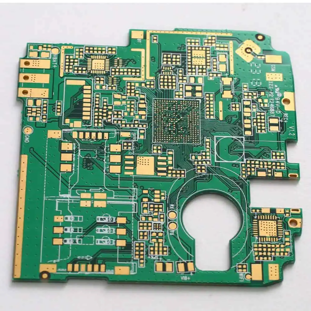
Understanding 6 Layer PCBs
A 6 layer PCB consists of six conductive copper layers separated by insulating material. This multilayer structure allows for higher component density and improved performance compared to simpler PCB designs. The layers typically include:
- Top layer
- Ground plane
- Power plane
- Signal layer 1
- Signal layer 2
- Bottom layer
This configuration provides excellent signal integrity, reduced electromagnetic interference (EMI), and better power distribution, making it ideal for complex IoT control applications.
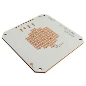
ENIG Surface Finish
ENIG is a popular surface finish for PCBs, especially in IoT applications. It involves depositing a layer of nickel, followed by a thin layer of gold on the exposed copper surfaces. Benefits of ENIG include:
- Excellent surface planarity
- Good solderability
- Long shelf life
- Suitable for fine-pitch components
- Resistant to oxidation
These characteristics make ENIG an excellent choice for IoT control boards that may require precise component placement and reliable connections.
Manufacturing Process
The manufacturing of 6 Layer ENIG IoT Control PCB boards involves several steps:
-
Design and File Preparation: The process begins with creating the PCB design using CAD software. The design is then converted into Gerber files, which contain all the necessary information for manufacturing.
-
Material Selection: High-quality substrate materials are chosen, typically FR-4 (Flame Retardant 4) or high-performance alternatives like Rogers or Taconic materials for specialized applications.
-
Inner Layer Processing: The inner layers (layers 2-5) are imaged, etched, and oxidized to create the circuit patterns and improve adhesion between layers.
-
Layer Lamination: The inner layers are stacked with prepreg (pre-impregnated bonding material) between each layer. This stack is then pressed under high temperature and pressure to form a solid board.
-
Drilling: Holes are drilled for vias, through-holes, and component mounting. This step requires high precision, especially for the small vias often used in IoT boards.
-
Plating and Filling: The drilled holes are plated with copper to create electrical connections between layers. Vias may be filled with epoxy resin for a smoother surface.
-
Outer Layer Processing: The outer layers (top and bottom) are imaged and etched to create the final circuit patterns.
-
Solder Mask Application: A solder mask is applied to protect the copper traces and prevent solder bridges during component assembly.
-
Surface Finish – ENIG Process: The ENIG process is applied:
- Microetching to clean the copper surface
- Catalytic treatment to prepare for nickel plating
- Electroless nickel plating
- Immersion gold plating
-
Silkscreen Printing: Component designators, logos, and other markings are printed on the board.
-
Electrical Testing: Each board is tested to ensure all connections are correct and there are no short circuits.
-
Cutting and Profiling: The individual boards are cut from the panel and shaped to their final dimensions.
IoT-Specific Considerations
When manufacturing PCBs for IoT control applications, several factors require special attention:
-
Signal Integrity: Proper layer stackup and impedance control are crucial for maintaining signal quality, especially for high-speed digital and RF signals common in IoT devices.
-
Power Management: Efficient power distribution is essential for battery-operated IoT devices. This may involve using entire layers for power and ground planes.
-
Thermal Management: IoT devices often need to operate in varied environmental conditions. Proper thermal design, including the use of thermal vias and copper pours, is important.
-
EMI/EMC Compliance: IoT devices must comply with electromagnetic compatibility regulations. Proper grounding, shielding, and layout techniques are employed to minimize EMI.
-
Size Constraints: Many IoT applications require compact designs. This necessitates the use of fine-pitch components and high-density interconnect (HDI) techniques.
-
Antenna Integration: For wireless IoT devices, antenna design and integration are critical. This may involve impedance-matched traces and clearances for antenna performance.
Quality Control and Testing
Rigorous quality control measures are implemented throughout the manufacturing process:
- Automated Optical Inspection (AOI): Used to detect defects in the copper patterns and solder mask.
- Flying Probe Testing: Ensures electrical connectivity and absence of short circuits.
- X-ray Inspection: Used for checking internal layers and plated through-holes.
- Cross-sectioning: Performed on sample boards to verify internal structure and plating quality.
- Solderability Testing: Ensures that the ENIG finish will accept solder properly during assembly.
Conclusion
The manufacturing of 6 Layer ENIG IoT Control PCB boards is a sophisticated process that combines cutting-edge technology with meticulous attention to detail. By leveraging the benefits of multilayer design and the ENIG surface finish, these PCBs provide the perfect foundation for creating robust, high-performance IoT control devices. As the IoT continues to evolve, PCB manufacturing techniques will undoubtedly advance to meet the growing demands of this exciting field.