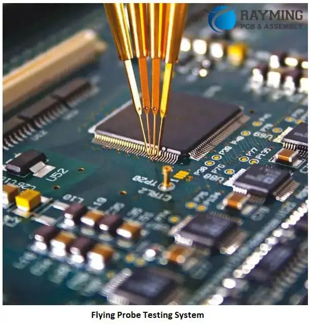
The production of a Printed Circuit Board (PCB) involves a crucial testing phase. It is essential that every PCB undergoes thorough testing to identify and address any electrical or circuit-related problems before it leaves the manufacturing facility. Common testing methods include In-Circuit Testing (ICT), Flying Probe Testing (FPT), and 4-wire Kelvin testing (particularly for PCBs used in automotive or aerospace applications).
Among these, Flying Probe Testing (FPT) has gained significant popularity due to its high precision and numerous advantages, especially with the growing demand for compact electronic devices. Let’s delve deeper into Flying Probe Testing and explore its benefits.

What is a Flying Probe Test?
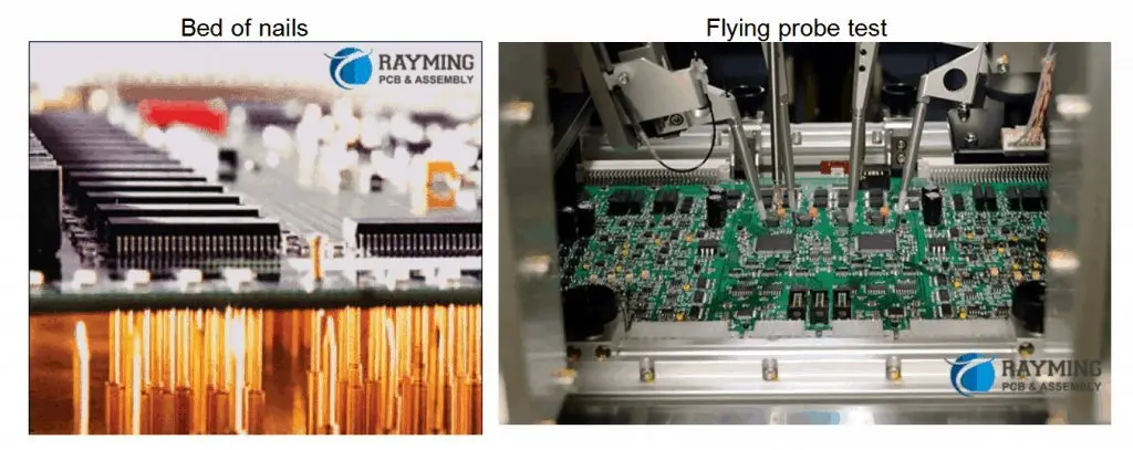
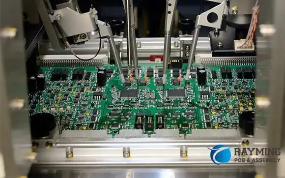
A flying probe test (FPT) is a highly flexible and precise method of testing printed circuit boards (PCBs) and printed circuit board assemblies (PCBAs). Unlike traditional bed-of-nails testing, which requires custom fixtures for each board design, flying probe testing uses mobile test probes that can move freely across the surface of the board.
These “flying” probes are controlled by high-precision motors and can access test points on the PCB with remarkable accuracy. The probes make contact with specific points on the board to perform various electrical tests, including continuity checks, short circuit detection, and component value measurements.
Flying probe testing is particularly valuable for:
- Prototyping and small production runs
- Testing complex or densely populated boards
- Verifying boards with limited access to test points
- Situations where fast setup times are crucial
The flexibility and precision of flying probe testing make it an indispensable tool in modern electronics manufacturing.
Guidelines for Test Point Design
To maximize the effectiveness of flying probe testing, it’s essential to consider several factors when designing test points on a PCB. Here are some key guidelines to keep in mind:
Accessibility to Nets
One of the primary considerations in test point design is ensuring that all critical nets are accessible to the flying probes. This involves:
- Strategic placement of test points across the board
- Avoiding obstruction by components or other board features
- Considering both top and bottom sides of the PCB for optimal coverage
Designers should work closely with test engineers to identify critical nets and ensure they can be reached by the flying probes.
Features of Test Points
The physical characteristics of test points play a crucial role in the success of flying probe testing. Key features to consider include:
- Size: Test points should be large enough for reliable probe contact but small enough to minimize board space usage. Typically, a diameter of 0.5mm to 1mm is suitable.
- Shape: Circular test points are most common, but other shapes may be used depending on the specific requirements of the test system.
- Surface finish: A smooth, flat surface ensures good electrical contact between the probe and the test point.
- Solder mask clearance: Adequate clearance around the test point prevents interference with probe contact.
- Labeling: Clear labeling of test points can facilitate easier programming and troubleshooting.
Board Clamping
Proper board clamping is crucial for accurate and reliable flying probe testing. Consider the following aspects:
- Clamping areas: Designate specific areas on the PCB for clamping, ensuring they don’t interfere with component placement or test points.
- Edge clearance: Maintain sufficient clearance from the board edges to accommodate clamping mechanisms.
- Stability: Ensure the clamping method provides stable support to prevent board flexing during testing.
- Compatibility: Consider the compatibility of the clamping method with both top and bottom side testing.
Board Dimensions
The physical dimensions of the PCB can impact the feasibility and efficiency of flying probe testing:
- Maximum board size: Ensure the PCB dimensions are within the working area of the flying probe tester.
- Minimum board size: Very small boards may require special fixturing or adapters.
- Thickness: Consider the board thickness in relation to the probe travel distance and clamping mechanisms.
- Warpage: Minimize board warpage to ensure consistent probe contact across the entire surface.
Maximum Component Height
The height of components on the PCB can affect the movement and accessibility of flying probes:
- Probe clearance: Ensure sufficient clearance for probes to move between components.
- Tall component placement: Consider strategic placement of tall components to minimize interference with probe movement.
- Dual-side testing: If testing both sides of the board, consider the cumulative height of components on both sides.
- Probe tip selection: Choose appropriate probe tips that can navigate around components of varying heights.
By carefully considering these guidelines during the design phase, engineers can significantly enhance the effectiveness and efficiency of flying probe testing.

How Does Flying Probe Testing Work?
Flying probe testing is a sophisticated process that involves several key steps. Understanding these steps can help engineers and manufacturers optimize their testing procedures and improve overall product quality.
1. Create an FPT Test Program
The first step in flying probe testing is creating a comprehensive test program. This involves:
- Design analysis: Studying the PCB design to identify all test points and critical nets.
- Test point mapping: Creating a precise map of all test points on the board.
- Test sequence planning: Determining the optimal sequence of tests to maximize efficiency.
- Probe movement optimization: Planning the most efficient path for probe movement across the board.
- Test parameter definition: Setting appropriate voltage levels, current limits, and measurement thresholds for each test.
Creating an effective test program requires a deep understanding of both the PCB design and the capabilities of the flying probe tester.
2. Upload the Program to the FPT Tester
Once the test program is created, it needs to be uploaded to the flying probe tester. This typically involves:
- File transfer: Securely transferring the test program files to the tester’s control system.
- Program verification: Running checks to ensure the program is compatible with the tester’s software and hardware.
- Calibration: Performing any necessary calibrations to ensure accurate probe positioning and measurements.
- Test run: Conducting a trial run to verify the program’s functionality and identify any potential issues.
3. Application of Electrical and Power Test Signals
With the program in place, the flying probe tester can begin the actual testing process:
- Board loading: The PCB is carefully loaded onto the test bed and secured.
- Probe positioning: The flying probes move to their initial positions based on the test program.
- Signal application: Electrical signals are applied to specific points on the board through the probes.
- Measurements: The tester measures various electrical parameters, such as voltage, current, resistance, and capacitance.
- Data analysis: The measured values are compared against expected values defined in the test program.
- Fault detection: Any discrepancies are flagged as potential faults for further investigation.
- Results logging: All test results are recorded for quality control and traceability purposes.
This process is repeated for all defined test points and sequences, providing a comprehensive evaluation of the PCB’s electrical integrity.
Why is This Type of Test Important?
Flying probe testing plays a crucial role in ensuring the quality and reliability of electronic products. Its importance stems from several key factors:
- Flexibility: FPT can adapt to different board designs without requiring custom fixtures, making it ideal for prototyping and small production runs.
- Precision: The high accuracy of flying probes allows for testing of densely populated boards and fine-pitch components.
- Cost-effectiveness: For low to medium volume production, FPT can be more cost-effective than fixture-based testing methods.
- Quick setup: The software-driven nature of FPT allows for rapid test program development and implementation.
- Comprehensive testing: FPT can perform a wide range of electrical tests, from basic continuity checks to complex functional tests.
- Non-destructive: Unlike some testing methods, FPT doesn’t require additional test points or modifications to the board design.
- Early defect detection: By identifying issues early in the production process, FPT helps reduce rework costs and improve overall product quality.
- Traceability: Detailed test results provide valuable data for quality control and continuous improvement efforts.
In an industry where product reliability is paramount and time-to-market pressures are intense, flying probe testing offers a powerful solution for ensuring electronic assemblies meet the highest standards of quality and performance.
10 Benefits of Flying Probe Testing
Flying probe testing offers numerous advantages that make it an attractive option for many electronics manufacturers. Here are ten key benefits:
- Flexibility: FPT can easily adapt to different board designs without requiring custom fixtures, making it ideal for prototyping and small to medium production runs.
- Cost-effectiveness: For low to medium volume production, FPT eliminates the need for expensive dedicated test fixtures, reducing overall testing costs.
- Quick setup time: Test programs can be developed and implemented rapidly, significantly reducing time-to-market for new products.
- High precision: Flying probes can access test points with exceptional accuracy, allowing for testing of high-density boards and fine-pitch components.
- Comprehensive testing: FPT can perform a wide range of electrical tests, including continuity, short circuit detection, component value measurement, and functional testing.
- Non-destructive testing: Unlike some testing methods, FPT doesn’t require additional test points or modifications to the board design, preserving the integrity of the original layout.
- Easy program modification: Test programs can be quickly modified to accommodate design changes or to focus on specific areas of concern.
- Reduced fixturing costs: The elimination of custom test fixtures not only reduces costs but also saves storage space and simplifies inventory management.
- Improved fault diagnosis: The precise nature of flying probe testing allows for accurate identification and localization of faults, facilitating easier troubleshooting and repair.
- Data collection and analysis: FPT systems typically provide detailed test results, enabling comprehensive quality control analysis and continuous improvement of manufacturing processes.
These benefits make flying probe testing an invaluable tool in the electronics manufacturing industry, particularly for companies dealing with diverse product lines or frequent design iterations.
PCB Flying Probe Test Vs. PCBA Flying Probe Test
While both PCB (Printed Circuit Board) and PCBA (Printed Circuit Board Assembly) flying probe tests use similar technology, they focus on different aspects of the manufacturing process. Understanding the differences between these two types of tests is crucial for implementing an effective quality control strategy.
PCB Flying Probe Test
PCB flying probe testing focuses on the bare board before components are mounted. Key characteristics include:
- Test focus: Primarily tests the integrity of the PCB itself, including copper traces, vias, and pads.
- Timing: Conducted after PCB fabrication but before component assembly.
- Test types:
- Continuity testing
- Short circuit detection
- Impedance testing
- High-voltage isolation testing
- Accessibility: Generally has full access to all test points on both sides of the board.
- Speed: Typically faster than PCBA testing due to fewer obstacles and test points.
- Fault types detected: Manufacturing defects in the PCB, such as open circuits, shorts, or incorrect impedance.
PCBA Flying Probe Test
PCBA flying probe testing is performed on assembled boards with components in place. Its characteristics include:
- Test focus: Evaluates both the PCB and the mounted components.
- Timing: Conducted after component assembly, often as a final quality check.
- Test types:
- All PCB tests
- Component presence and orientation
- Component value verification
- Functional testing of active components
- Accessibility: May have limited access to some test points due to component placement.
- Speed: Generally slower than PCB testing due to more complex test sequences and potential obstacles.
- Fault types detected: PCB manufacturing defects, component placement errors, faulty components, and assembly issues.
Key Differences
- Scope: PCB testing is more limited in scope, focusing solely on board integrity, while PCBA testing provides a comprehensive evaluation of the entire assembly.
- Complexity: PCBA testing is typically more complex due to the presence of components and the need for more sophisticated test sequences.
- Test point access: PCB testing usually has better access to test points, while PCBA testing may require careful probe navigation around components.
- Fault detection: PCBA testing can detect a wider range of faults, including issues related to component assembly and functionality.
- Test program development: PCBA test programs are generally more complex and may require more time to develop and optimize.
- Cost: PCB testing is often less expensive due to its simpler nature and faster execution.
- Stage in manufacturing process: PCB testing occurs earlier in the process, allowing for defect detection before valuable components are added.
Both PCB and PCBA flying probe tests play crucial roles in ensuring the quality of electronic products. PCB testing helps catch defects early in the manufacturing process, potentially saving costs by preventing the assembly of components onto faulty boards. PCBA testing provides a final quality check, ensuring that the completed assembly meets all specified requirements.
In many cases, manufacturers may choose to implement both types of testing at different stages of production to maximize quality control and minimize the risk of defective products reaching the end-user.
Conclusion
Flying probe testing has established itself as a critical tool in the electronics manufacturing industry. Its flexibility, precision, and cost-effectiveness make it particularly valuable for prototyping, small to medium production runs, and testing complex or densely populated boards.
By following best practices in test point design and understanding the nuances of both PCB and PCBA flying probe testing, manufacturers can leverage this technology to improve product quality, reduce time-to-market, and enhance overall manufacturing efficiency.
As electronics continue to become more complex and miniaturized, the role of flying probe testing is likely to grow even more significant. Its ability to adapt to new designs and technologies positions it as a key player in the future of electronics quality assurance.
Whether you’re a design engineer, a quality control specialist, or a manufacturing manager, understanding the capabilities and benefits of flying probe testing can help you make informed decisions about your testing strategies and ultimately contribute to the production of higher-quality electronic products.