
RAYPCB / Flexible circuits
Single-Sided Flexible PCB Manufacturing
One copper layer for a thin, clearly defined interconnect.
Share your drawings, quantities and mechanical requirements for an engineering-reviewed quote. You can contact us directly without completing the optional tools.
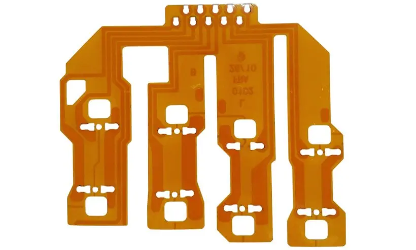
Single-Sided Flexible PCB — design decisions
A single-sided flexible PCB carries one patterned copper layer on a flexible dielectric. It is useful when the net routing can remain on one layer and a second layer would add thickness without solving a real routing requirement. Exposed contacts can have local reinforcement while the cable region remains flexible.
| Decision | Specify | Review |
|---|---|---|
| Routing | Trace width, clearance and any shielding requirement | One layer cannot provide independent crossing traces without changing the interconnect approach. |
| Contact access | Exposed-pad side, contact finish and connector part number | Do not confuse access from two faces with two copper layers. |
| Bend region | Finished thickness, bend direction and installed radius | Keep the thickness calculation local to the moving or formed region. |
| Reinforcement | Stiffener outline, material, adhesive and thickness | Connector thickness is a local mechanical requirement. |
If routing needs a second copper layer, compare double-sided flexible PCB. More layers should solve a routing or return-path problem, rather than being added as a general upgrade.
One copper layer does not mean every opening is on one side
| Top-to-bottom order | Construction note |
|---|---|
| Top coverlay | PI film + bonding adhesive; openings only where required |
| Copper L1 | Specify finished copper and function; do not assume every layer is a plane |
| Bottom surface | PI substrate |
A single conductor layer can serve contacts exposed through selected openings, but exposing both sides of a conductor is not the same as adding a second copper routing layer. Show the access side and protection boundaries on the drawing. A local stiffener adds mechanical support, not circuitry.
If crossing nets require a second conductor layer or plated interconnections, compare double-sided flex manufacturing rather than describing the job as a single-layer circuit.
Relevant construction examples

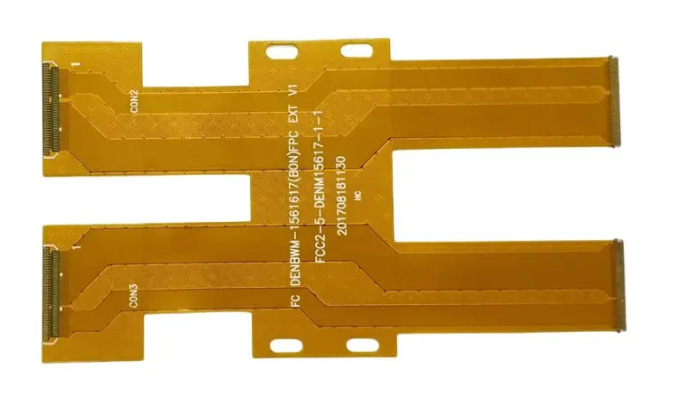
Where one layer needs careful detailing
Document exposed copper openings and the transition between the supported contact area and the free flex. A stiffener can help a connector or component area, but the edge also defines a mechanical transition. Avoid assuming that a smaller bend radius is acceptable simply because the circuit has one copper layer.
For repeated motion, identify the moving length, bend direction, installed radius, temperature and required cycles in the enquiry. Copper type alone does not determine life. The calculator deliberately returns geometry instead of a fatigue-life promise.
Material selection starts with the actual laminate, copper and coverlay grades. Refer to DuPont’s laminate portfolio and the supplier drawing for each selected grade. Kapton and Pyralux are not interchangeable names for every flexible circuit material.
Flex design & project planning
Check bend-region thickness and the local connector stack separately. Enter the actual supplier values; do not count stiffeners as part of a flexible bend.
RAYPCB ENGINEERING
Project PreparationFlexible PCB Design Workbench
Loading Flexible PCB Design Workbench…
Optional bare-flex budget
Choose the construction independently from the design check. This is an early budget scenario; it does not price a validated stackup.
RAYPCB ENGINEERING
Project PreparationFlexible PCB Budget Estimator
Loading Flexible PCB Budget Estimator…
Prepare the next engineering review
Send the available files even if some decisions remain open. Mark the points where you need advice.
- Gerber or agreed fabrication data, outline drawing and drill data where applicable.
- Layer stackup, material grades, finished thickness and tolerances.
- Bend zones, installed radius, motion duty, coverlay openings and reinforcement drawing.
- Connector requirements, order quantities and requested delivery.
Download calculator results if you want to include them. Contact inputs are not automatically filled from these tools.
Practical questions
What is the first decision for this construction?
Resolve single-layer contact openings before treating the layer count as a complete specification. Include the mechanical drawing and identify any unknowns.
Does the design tool approve the bend radius?
No. It checks the entered geometry and planning assumptions; it does not predict fatigue life or release the construction for manufacture.
Is the displayed budget an exact quote?
No. The model is uncalibrated. Unsupported or complex constructions need manual review. Send the files for an exact quotation without completing the calculator if you prefer.