
RAYPCB · Surface engineering
OSP PCB Surface Finish: IPC-4555, Assembly & Cost
OSP protects exposed copper with a thin organic film before soldering. It can offer flat pads and economical processing when storage, handling and the complete assembly sequence are controlled. The useful specification is a qualified coating-and-assembly window, not simply the lowest-cost finish name.
Send preliminary files or an existing fabrication note. Identify the finish decision you need help resolving.
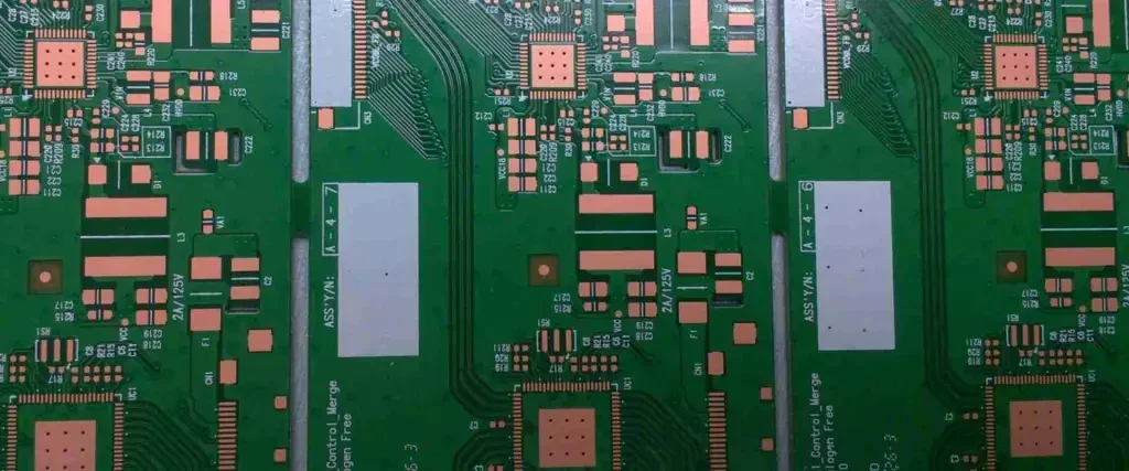
A clear starting point for the finish decision
| Specification item | How to use it |
|---|---|
| Finish system | OSP |
| Standards map | IPC-4555 high-temperature OSP; J-STD-003 solderability |
| Thickness planning | Chemistry-dependent thin organic film; agree the supplier measurement method and qualified coating window. |
| Main cost drivers | Low precious-metal cost; packaging, timing, exposure and rework affect the complete build. |
| Acceptance basis | Ordered revision, drawing, measurement, sampling and application-specific evidence. |
Thickness examples and selection guidance are not a complete IPC acceptance specification. State the contracted revision, measurement basis, sampling and application requirements on the order.
Shortlist by the interface your product needs
Choose the primary interface and the constraints that matter. The selector explains candidates and open questions; it does not rank finishes by a fabricated quality score. You can open the relevant finish page or go directly to an enquiry.
RAYPCB ENGINEERING
Surface FinishPCB Surface Finish Selector
Loading PCB Surface Finish Selector…
What an organic solderability preservative does
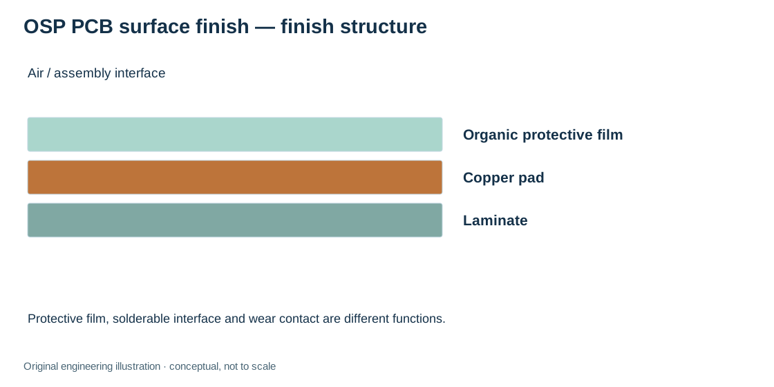
OSP means organic solderability preservative. The finish forms a protective organic film on exposed copper rather than adding a nickel or precious-metal stack. During the qualified soldering process, flux and thermal exposure allow the solder to wet the copper. The coating therefore serves a temporary protection function within a defined manufacturing and logistics route.
OSP is not soldermask or a permanent conformal coating. Soldermask controls exposed regions; OSP protects the copper within those regions before assembly. The board can look copper-coloured, but appearance does not establish film thickness, chemistry or remaining solderability. The finish follows the underlying topography and does not correct recessed features or warpage.
For dense solderable layouts, that lack of a thick metal buildup can be useful. The decision still needs assembly evidence. A flat finish does not compensate for an unsuitable stencil, an open via draining solder or a poorly controlled reflow profile. Use OSP as one part of the board-and-assembly system, with the coating and downstream operations qualified together.
Storage and assembly date planner
Enter the start of the relevant approved window, the last planned use date and the supplier-approved day limit. Calendar margin = approved days − elapsed days. The limit is not prefilled because it depends on chemistry, packaging and exposure.
RAYPCB ENGINEERING
Surface FinishSurface Finish Engineering Workbench
Loading Surface Finish Engineering Workbench…
From surface preparation to a controlled release
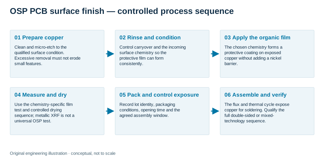
Follow the sequence below. The optional step player is a conceptual explanation, not factory footage or a production recipe.
- Prepare copper
Clean and micro-etch to the qualified surface condition. Excessive removal must not erode small features.
- Rinse and condition
Control carryover and the incoming surface chemistry so the protective film can form consistently.
- Apply the organic film
The chosen chemistry forms a protective coating on exposed copper without adding a nickel barrier.
- Measure and dry
Use the chemistry-specific film test and controlled drying sequence; metallic XRF is not a universal OSP test.
- Pack and control exposure
Record lot identity, packaging conditions, opening time and the agreed assembly window.
- Assemble and verify
The flux and thermal cycle expose copper for soldering. Qualify the full double-sided or mixed-technology sequence.
IPC-4555 and the chemistry-specific coating window
The appropriate finish reference is IPC-4555, the performance specification for high-temperature OSP. The official IPC-4555 contents covers coating, measurement, solderability, storage and other performance topics. IPC-4552 is the ENIG specification; it should not be substituted as an OSP thickness reference.
OSP chemistries do not all use one universal film thickness. Agree the chemical system, supplier operating window and measurement method. A commonly repeated numerical range from another chemistry is not automatically transferable. Too little or too much coating can create different process concerns, so “thicker is safer” is not an adequate instruction.
Use an appropriate organic-film measurement technique. Standard metallic-finish XRF settings are not a universal way to establish the OSP film. Keep coating results separate from copper thickness measurements and from actual solderability evidence. The release should identify what is controlled by the finishing process and what is verified after the agreed storage or thermal conditioning.
Modern OSP is not limited by a universal reflow count
Different OSP systems have different qualified thermal capabilities. The chemical supplier's OSP information describes systems developed for multiple lead-free reflows. That does not justify a blanket promise that every OSP board can tolerate any number of reflows, but it also means that a universal “one reflow only” rule is misleading.
Plan the actual sequence: first-side reflow, second-side reflow, selective soldering and any repair. Include which pads remain unsoldered during earlier heat exposures. Their final soldering condition may matter more than the condition of pads already covered by solder. Tell the fabricator and assembler about that sequence before agreeing the finish.
Qualify the coating with the flux, atmosphere, thermal profile and handling used in production. If the route changes, review whether existing evidence still applies. A new rework step or a longer hold can change the condition at the last soldering operation. Keep process changes visible rather than assuming the original OSP approval covers every future variation.
Storage planning: sealed life and open exposure are different
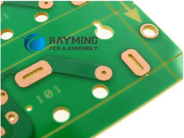
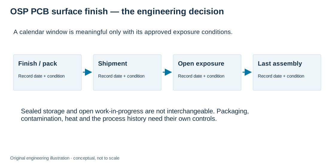
An OSP board may spend time in sealed packaging, incoming inspection, an open tray and partially completed assembly. These periods are not equivalent. Record the fabrication lot, packaging instructions, opening date and the planned last soldering operation. Follow the qualified conditions supplied for that finish chemistry and the product.
The schedule tool compares calendar dates with a user-entered permitted window. It does not predict oxidation or infer a universal shelf life from the finish name. A positive number of days remaining is useful only if packaging, environment and exposure assumptions remain valid. If those conditions are unknown, treat the result as a planning reminder and obtain a review.
Handle boards by appropriate edges with the approved precautions. Fingerprints, incompatible cleaners and repeated unwrapping can change the surface. Do not automatically bake, polish or chemically clean a suspect OSP lot using a generic repair recipe. Additional heat or chemistry may affect the coating and solderability. Ask for a finish-specific disposition supported by the actual lot condition.
Design for probing, press-fit and mixed interfaces
OSP is primarily selected for a protected solderable copper interface. It is not a wear-resistant sliding contact finish. Test probing, connector insertion and bonding each require their own review. A board electrically tested once at fabrication presents a different contact task from a product test pad probed repeatedly through production and service.
If a connector relies on a particular finished-hole or contact surface, follow its specification rather than assuming OSP is interchangeable with tin, silver or gold. Press-fit performance depends on hole dimensions, plating and the compliant-pin system. A finish name alone cannot approve the connector interface.
Mixed OSP and selective gold constructions also need process planning. The IPC-4555 contents explicitly identifies mixed-finish and galvanic-corrosion topics. Define the zones and ask about sequence, transitions and compatibility. Do not add selective gold after routing without checking the manufacturing consequences. Where a flat metallic finish better serves the handling or interface need, compare ENIG using the same board and assembly scope.
Cost advantage depends on the complete production route
OSP does not require a precious-metal deposit, which can make it attractive for cost-sensitive assemblies. The actual quote still reflects setup, panel handling, inspection, packaging and order size. A finish-line saving is not the same as a guaranteed reduction in total product cost.
Include the logistics needed to preserve the qualified surface. Smaller delivery lots, controlled work-in-progress, appropriate packaging and a defined action for overdue material may be important. Those controls can be entirely practical for a stable production line, while a product with uncertain assembly timing may benefit from a different finish strategy.
Use the budget tool to compare actual entered allowances and keep the assumptions visible. Do not assign a guessed failure rate to OSP or assume another finish eliminates all assembly defects. If the production schedule is stable, quote OSP against an alternative with the same inspection and delivery scope. If timing is uncertain, ask for a technical and commercial comparison before choosing on unit price.

Prepare an OSP fabrication and assembly brief
Name the OSP requirement and the agreed standard revision, then state the assembly sequence and logistics. Include board quantity, critical footprints, unsoldered pads exposed to prior heat, test access and any selective finish. Where the chemistry is not fixed, identify the thermal and storage performance that the supplier needs to support.
Request a clear definition of the permitted storage and open-exposure conditions and the action required when they are exceeded. Record whether solderability testing, conditioning or other evidence is included. A useful acceptance plan provides a way to resolve an overdue or mishandled lot instead of leaving the receiving team with only a generic expiry date.
Send the files directly to RAYPCB for an OSP review when you already know the intended route. If you also need the board assembled, coordinate the finish with the PCB Assembly service before fabrication release. For an earlier selection decision, return to the surface finish comparison and compare OSP with the handling and interface requirements of the actual product.
Compare finish allowances and prepare a useful RFQ
Use the same quantity, currency and included scope for both options. Enter a bare-board allowance only if you want it included; leaving it blank produces a finish-only comparison. Setup and inspection or packing are lot charges, while the finish allowance is per board. Enter zero only for a confirmed zero or already-included item.
The comparison exposes the arithmetic behind your inputs. It does not estimate a supplier tariff, promise a yield saving or approve a complex selective-finish route. Changing quantity or finish choice clears the affected allowances so an old assumption is not silently carried into a new scenario. Exact quotes require fabrication files and an agreed finish specification.
RAYPCB ENGINEERING
Surface FinishSurface Finish Cost Comparison
Loading Surface Finish Cost Comparison…
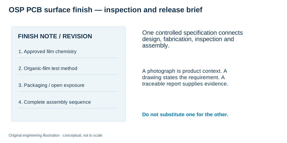
Keep the finish requirement with the design revision
| Include in the enquiry | Why it matters |
|---|---|
| Fabrication files, revision and quantity | Keeps the quotation tied to the correct geometry and build. |
| Finish system and selective area map | Separates solder, bond and contact functions. |
| Standard revision, metal / film requirement and method | Makes the acceptance requirement interpretable. |
| Assembly sequence, storage and service exposure | Identifies the condition in which the interface must function. |
| Required reports and open decisions | Distinguishes supplied evidence from qualification still needed. |
Use the tool download or email draft to carry the current inputs into a discussion. Attach your fabrication data separately. The Contact button opens the enquiry page; it does not automatically transfer calculator parameters or upload files. Preliminary information is welcome when the finish still needs to be selected.
Questions engineers and buyers ask
Which IPC standard applies to OSP?
IPC-4555 addresses high-temperature OSP. Use the contracted revision and the qualified chemistry and measurement requirements.
Can OSP support double-sided reflow?
Some qualified OSP systems support multiple lead-free reflows. Validate the actual chemistry and complete sequence rather than using a universal cycle count.
Can I use the date tool to certify solderability?
No. It checks your entered schedule against your entered window. It cannot measure oxidation, coating condition or solderability.
Is OSP appropriate for repeatedly mating contacts?
Do not use it as a generic wear-contact finish. Specify the contact function and select a qualified interface.
Continue with a related finish decision
Standards and original technical references
These references support scope and engineering context. Public previews do not contain every licensed acceptance clause. Use the ordered standard revision, agreed drawing and qualified supplier process for production acceptance.

