
RAYPCB · High-speed channel planning
MEGTRON PCB: design to a channel budget
Select Panasonic MEGTRON by full grade and construction, then allocate channel loss across traces, connectors and vias. Keep material data and manufactured-board evidence connected.
Preliminary material choices and open construction questions are welcome.
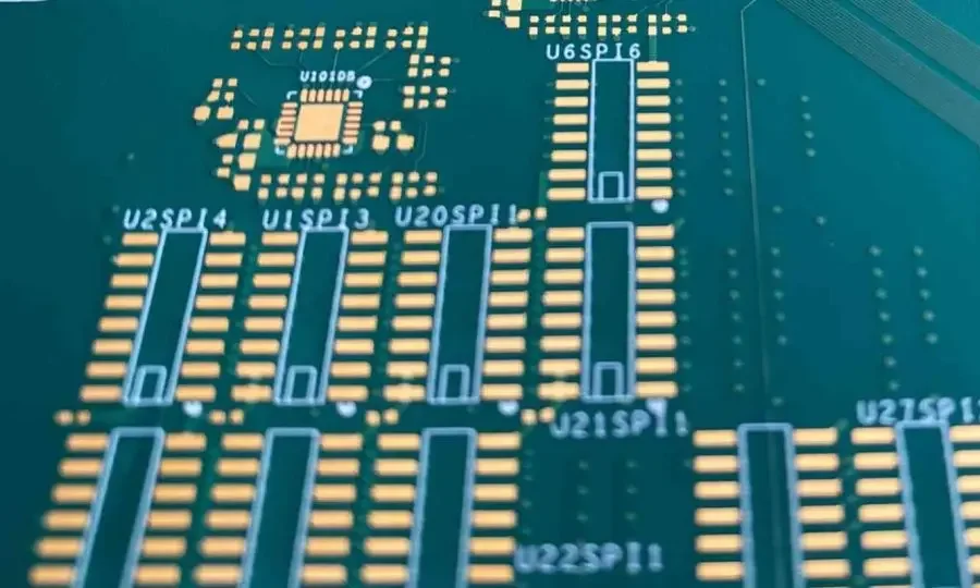
What is a MEGTRON PCB?
A MEGTRON PCB uses a specified Panasonic MEGTRON laminate and bonding construction, commonly for high-speed digital or low-loss interconnect applications. MEGTRON is a material family, not a finished-board performance grade. The full series, product suffix, glass system, resin content, copper profile and stackup determine which material data applies. A board does not gain a guaranteed data rate merely because its drawing says MEGTRON 6, 7 or 8.
For a design engineer, the practical task is to choose a manufacturable construction that leaves enough electrical margin for the complete channel. For a buyer, it is to obtain comparable quotations against that same construction. This page connects those tasks: interpret the supplier's material data, allocate channel losses, identify manufacturing variables and prepare a material-specific RFQ. Existing RF PCB services remain the route for a broader manufacturing review across brands.
Start with the complete channel, then select the laminate
A high-speed path can contain packages, PCB traces, vias, connectors and another board. The system requirement applies to that path under defined conditions. If the trace consumes nearly all of an insertion-loss allowance, a nominally lower-loss laminate may help. If a resonant via or connector launch dominates the response, changing the resin system alone may leave the actual problem unresolved.
Write down the required frequency range and the reference planes of the channel requirement. For a serial interface, symbol rate, modulation, equalization and the applicable compliance method matter; the word “high speed” is not a specification. Do not use the highest clock frequency as a universal signal-bandwidth limit. Record the actual channel model or test definition that the design must meet.
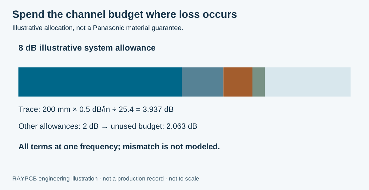
The example above allocates an 8 dB allowance at one chosen frequency. A 200 mm trace at an entered 0.5 dB/in contributes 3.937 dB. Adding 1 dB for connectors, 0.7 dB for vias and 0.3 dB for other included effects gives 5.937 dB, leaving 2.063 dB by scalar arithmetic. These are illustrative allowances, not Panasonic test results or a prediction for a particular RAYPCB board.
Build a transparent channel-loss allocation
Use this worksheet when you have an attenuation rate from a relevant measurement or model and want to understand how much allowance the routed length consumes. Enter all terms at the same evaluation frequency. The tool shows the trace contribution, non-trace contributions, remaining budget and the trace length that would consume the remaining allowance. A negative margin is visible without hiding it behind a “recommended material” badge.
RAYPCB ENGINEERING
RF Material FamiliesMEGTRON Channel Loss Allocation
Loading MEGTRON Channel Loss Allocation…
This is a scalar planning calculation. Adding dB allowances is not equivalent to cascading full S-parameters when mismatch and reflections matter. The result excludes effects not represented in the inputs, and a positive remainder is not an interface-compliance result. For detailed routing decisions, combine the allocation with controlled impedance planning and the actual channel simulation. If via stubs are a concern, discuss the geometry through the back drilling page rather than assigning every via the same loss.
Read MEGTRON series, suffixes and conditions together
The Panasonic MEGTRON family directory is the starting point for current product documents. A family comparison can narrow a shortlist, but it does not replace a construction-specific stackup. Keep the exact laminate and prepreg product codes on the drawing. Where a product has multiple glass or copper options, keep the suffix through purchasing, fabrication and change control.
| Selection level | What it helps establish | What it does not establish alone |
|---|---|---|
| MEGTRON family or series | A route to relevant supplier products and documents | Finished-board attenuation or a supported data rate |
| Full product and suffix | The intended variant and available construction context | Your pressed dielectric thickness or trace geometry |
| Glass, resin and copper | The actual stackup ingredients and roughness context | A validated model of connectors, vias and packages |
| Measured channel or coupon | Performance of a defined specimen under stated conditions | Every board geometry or every operating environment |
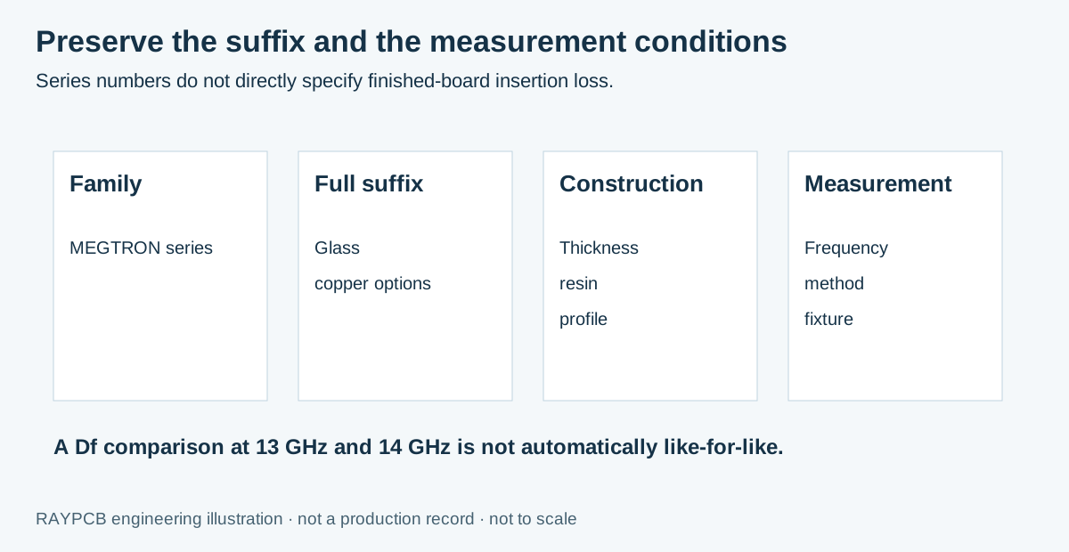
Panasonic's MEGTRON 7 product information distinguishes variants rather than publishing one universal MEGTRON 7 number. Some tabulated values use different glass systems and measurement frequencies. Those conditions are part of the data. A Df measured at 13 GHz should not be silently ranked against another candidate measured at 14 GHz as though both represented an identical test. Request a common comparison basis when the difference is important to the decision.
For a newer series such as MEGTRON 8, review the current product construction and fabrication fit before using a “newer is better” shortcut. A lower typical dielectric loss may have little economic value on a short path with ample margin. A longer or more constrained channel may justify it. The appropriate choice follows the requirement and manufacturing evidence, not the series number by itself.
For a project narrowed to this series, use the MEGTRON 6 grade and stackup review to identify glass and foil variants before comparing the channel model. The series name alone does not define an approved construction.
Copper profile and geometry belong in the material decision
The laminate dielectric is only one contributor to trace attenuation. Copper roughness and conductor geometry affect conductor loss, particularly as frequency rises. A supplier's test coupon may use a copper profile or dielectric thickness different from the proposed board. Importing its attenuation rate into another geometry without adjustment can create an optimistic budget.
Ask which copper foil and treatment are available in the requested construction. Distinguish nominal starting copper from finished outer-layer copper after processing. Width, etch shape, dielectric spacing and reference-plane geometry all enter the transmission-line model. For a fine-pitch escape region, the geometry that satisfies routing density may be narrower and lossier than the long-route geometry, so a single board-wide dB/in value may be inadequate.
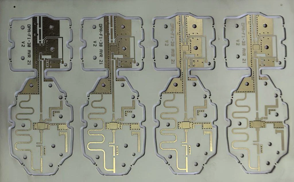
The RF panel photograph illustrates why conductor shapes and transitions deserve attention; it is not MEGTRON qualification evidence. A practical layout review identifies uniform line sections separately from launches, branches, vias and bends. For mixed-material designs, use the high frequency material comparison guide to check whether a hybrid route serves the actual circuit instead of placing an expensive material everywhere by default.
Design a stackup that can be quoted and repeated
Begin with the electrical layer functions, references and thickness target. Then choose available cores and prepreg constructions with the fabricator. A nominal finished thickness does not uniquely determine glass style, resin content or the spacing around a signal layer. Changing the pressed dielectric to meet mechanical thickness can also change impedance and loss, so the mechanical and electrical constraints must be reconciled together.
Include copper balance, plane distribution and the proposed via architecture. Sequential lamination, filled structures or unusual board thickness can influence process risk and quote scope independently of the MEGTRON family. The multilayer PCB planning page provides the layer-function framework; this page adds the grade and channel evidence needed for material selection.
Where a design permits alternatives, define the comparison process instead of writing “MEGTRON or equivalent” with no acceptance basis. An alternative may require revised widths or a different core/prepreg combination. Request a separate proposed stackup, updated electrical assessment and explicit approval. A procurement substitution should never be assumed to preserve channel behavior automatically.
Agree coupon and measurement boundaries before fabrication
The strongest acceptance discussion starts before the board is built. State the intended characteristic: impedance, insertion loss, dimensional geometry, thermal reliability or another requirement. Identify the measurement method, coupon design, frequency range, reference planes, sample scope and reporting format. A certificate stating the material family is not a substitute for those measurements.
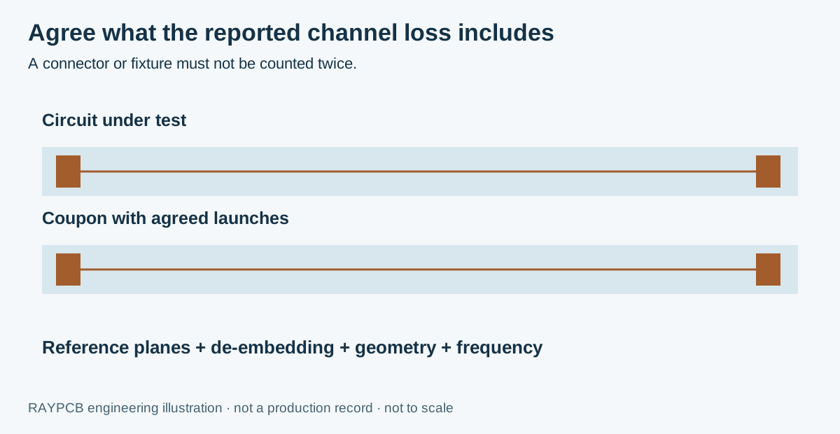
If attenuation comes from a measured coupon, understand whether the reported value includes launches and fixture effects. De-embedding and extraction choices determine how the data can be reused. Do not enter a connector allowance again if the line attenuation already includes the same connector. Conversely, a dielectric-only estimate must not be presented as the full channel insertion loss.
Retain the material and stackup revision with the results. If the layout, copper option, glass construction or finish changes, assess whether the old evidence still applies. A repeat order is easiest to manage when the approved construction, fabrication files and test requirements are linked by one release revision. Use PCB DFM review to resolve build questions before locking the purchasing specification.
What drives MEGTRON PCB cost?
Material grade and construction availability matter, but cost also follows panel utilization, copper layers, board dimensions, drilling and lamination sequence, finish, testing and the quantity over which setup is distributed. A material upgrade can be economical if it avoids a more complex channel or reduces a critical design risk. It can also add cost without useful benefit when the original channel already meets its requirement.
Compare options on the same finished-board specification. If one quotation includes insertion-loss coupons and another includes only electrical continuity testing, their totals do not represent the same purchase. Separate one-time engineering and tooling allowances from repeat-board cost, and keep freight, tax, components and assembly exclusions visible. Current material stock and production timing require a project-specific confirmation.
RAYPCB ENGINEERING
RF Material FamiliesMEGTRON Material Budget and RFQ Brief
Loading MEGTRON Material Budget and RFQ Brief…
The budget tool accepts your own per-board, setup and verification allowances. It can also produce an RFQ brief with all costs left blank. It contains no automatic MEGTRON price table or universal multiplier. For a firm quotation, send the full product callout, proposed stackup, fabrication data, quantity and required evidence through RAYPCB manufacturing review. Downloaded worksheet parameters must be attached manually.
MEGTRON design and sourcing questions
Is MEGTRON only for RF circuits?
No. The family is also used in high-speed digital interconnect contexts. Select according to the electrical channel and product construction rather than the label RF or digital. The relevant frequencies, losses, references and manufacturing requirements still need definition.
Can the channel tool choose MEGTRON 6, 7 or 8 for me?
No. It allocates loss using the attenuation data you enter. The selection requires matched-condition data for the proposed construction, the complete channel requirement, availability and fabrication review. An automatic series recommendation without those inputs would imply more certainty than the model supports.
Is the lowest Df always the lowest-cost design?
No. The total cost depends on board construction and the value of the resulting margin. Copper, geometry, vias and connectors can dominate the remaining problem. Compare complete design options and measurement scope, not just the laminate's typical Df.
What information makes a quotation useful?
Provide the complete MEGTRON product and suffix if fixed, or a requirements-led shortlist if it is still open. Include the layer stack, dimensions, finished copper, quantity, channel evaluation conditions and verification scope. Identify allowable alternatives and who must approve them.
Discuss a MEGTRON stackup
Send the exact material callout or your shortlist, drawing revision, construction, quantity and the main unresolved engineering question. Include the measurement or qualification scope you need.
Tool use is optional. Attach any downloaded brief manually; Contact does not automatically receive worksheet inputs. References reviewed September 2026. Illustrations are explanatory, and photographs are not process qualification records.

