Introduction
Printed circuit boards (PCBs) have evolved from simple single or double layer boards to complex multilayer boards with 6 or more layers to accommodate increasing component density and interconnectivity needs. 6 layer PCBs provide more flexibility for routing, plane separation and enable partitioning of circuits across layers.
However, designing the 6 layer stackup requires careful planning to utilize the layers effectively and avoid signal integrity issues. Key considerations include layer sequence, reference planes, material selection, copper weights, trace routing and via design. This article provides a detailed overview of 6 layer PCB stackup configurations, thickness calculations and manufacturing processes.
6-Layer PCB Stackup Selector 6L
Configure layer thicknesses for your 6-layer PCB stackup
Copper Layers
Prepreg Layers
Core Layers
| Component | Thickness |
|---|---|
| Copper (6 layers) | 210 µm |
| Prepreg (3 layers) | 456 µm |
| Core (2 layers) | 400 µm |
Stackup Visualization
1.2mm: Standard thin multilayer
1.6mm: Most common thickness
2.0mm: Power applications, thermal management
L3 & L4: Inner signal layers – route high-speed signals here for protection.
6 Layer PCB Stackup Configuration
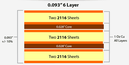
The 6 conductive copper layers in a multilayer PCB are arranged in a predetermined sequence along with dielectric materials separating them. This is referred to as the layer stackup. Some key guidelines for 6 layer stackup design:
Layer Sequence
The conductors are numbered sequentially with the topmost layer being Layer 1. A typical 6 layer board stackup has:
Layer 1: Top/Component layer
Layer 2: Reference plane 1
Layer 3: Signal/Plane layer 2
Layer 4: Signal/Plane layer 3
Layer 5: Reference plane 2
Layer 6: Bottom layer
The top and bottom layers are used for component placement and routing. The inner layers are used for signals and reference planes.
Reference Plane Placement
The reference planes (ground and power) should be adjacent to routing layers for controlled impedance. A continuous ground plane next to signals is highly recommended.
Plane Splits
Reference planes can be split into analog and digital power sections to provide clean isolated supplies to sensitive analog circuits.
Symmetry
Symmetrical arrangement with reference planes above and below the mid layer provides optimal signal integrity. Asymmetrical stackups also used when needed.
Signal Routing
Route critical high speed or noise sensitive signals on inner layers sandwiched between planes. Avoid routing them on outer layers.
Breakout Vias
Use breakout/stub vias when routing inner layer traces to outer layers. Confines any stub effects.
Minimum Spacing
Follow board fabricator's design rule check (DRC) guidelines for minimum trace width, spacing, annular rings.
Common 6 Layer Stackup Arrangements
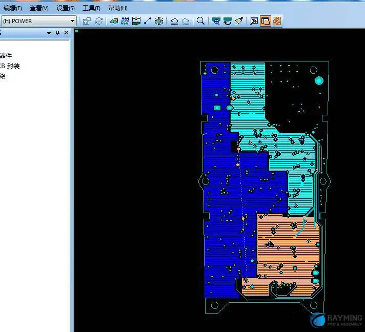
1. Symmetrical Arrangement
Copy code
Layer 1: Signal Layer 2: Ground Layer 3: Signal Layer 4: Power Layer 5: Signal Layer 6: Ground Layer 7: Signal
- Identical reference planes above and below mid layer
- Excellent signal integrity performance
- Widely used for digital, analog, RF designs
2. Asymmetrical Arrangement
Copy code
Layer 1: Signal Layer 2: Ground Layer 3: Signal Layer 4: Power Layer 5: Power Layer 6: Ground Layer 7: Signal
- Permits splitting power plane into sections
- Discontinuous ground planes affect signal quality
- Used when power distribution needs warrant it
3. Hybrid Arrangement
Copy code
Layer 1: Signal Layer 2: Ground Layer 3: Signal Layer 4: Ground Layer 5: Power Layer 6: Ground Layer 7: Signal
- Top and bottom ground planes for signals
- Mid power plane for splitting
- Balances signal integrity and power needs
6 Layer PCB Stackup Thickness Considerations
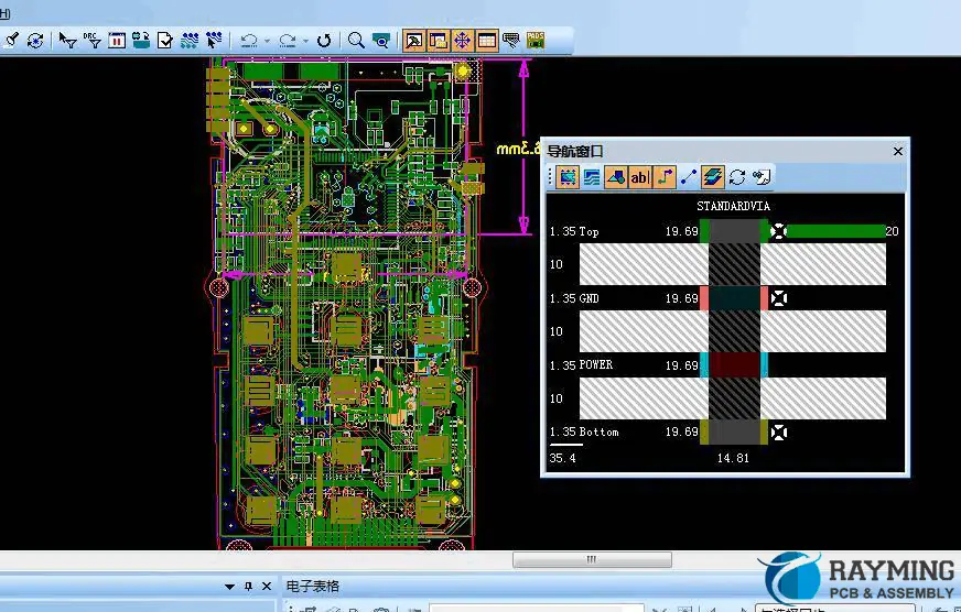
The overall thickness of a 6 layer PCB depends on:
- Copper layer thickness
- Dielectric layer thickness
- Number of lamination cycles
Copper Layer Thickness
Typical copper weights:
- Outer layers : 1 oz (35 μm)
- Inner layers: 1 oz or 0.5 oz (18 μm)
- Plane layers: 2 oz (70 μm) recommended
Heavier copper allows higher current carrying capacity.
Dielectric Layer Thickness
Typical dielectric layer thickness:
- 8 mil to 14 mil per layer
- 112-170 μm glass epoxy FR4 material
- Thinner dielectrics help minimize layer to layer capacitance
Lamination Cycles
A 6 layer board can be fabricated by:
- 2 lamination cycles - Bottom 3 layers pressed first, then top 3 layers
- 3 lamination cycles - Bottom 2, mid 2 and top 2 layers bonded
2 lamination cycles results in lower thickness variation versus 3 cycles.
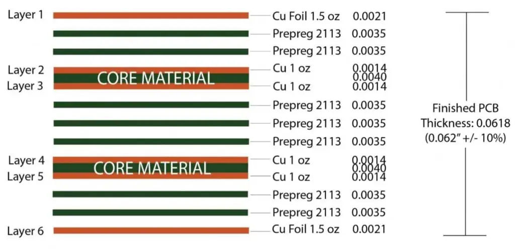
Example 6 Layer PCB Stackup Thickness
Here is a sample 6 layer PCB stackup with typical thickness values:
Copy code
Layer Type Thickness Layer 1 - Top Signal 1 oz (35 μm) Layer 2 Ground 2 oz (70 μm) Layer 3 Signal 1 oz (35 μm) Layer 4 Signal 1 oz (35 μm) Layer 5 Power 2 oz (70 μm) Layer 6 - Bottom Signal 1 oz (35 μm) Dielectric 10 mil (254 μm) Total Thickness 6 Layers 110 mils (2.79 mm)
This is a symmetrical arrangement with approximately 110 mils (2.79 mm) total board thickness. Thinner dielectrics or copper can be used to reduce overall thickness. 8 layer boards typically range from 130 mils to 200 mils thickness.
6 Layer PCB Design and Manufacturing Process
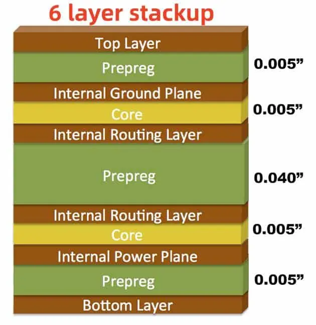
The typical workflow for assembling a 6 layer PCB is:
1. Design
- Create schematic, layout, stackup in PCB design software
- Floorplan components, route traces, assign plane layers
- Design rule checks, signal integrity simulations
- Panelization, generate Gerber and drill files
2. Fabrication Data
The board fabricator reviews:
- Layer stackup and netlist
- Material selection
- Trace widths, spacing, annular rings
- Hole sizes, drill data, test points
- Panel drawing, breakaway tabs, fiducials
3. Inner Layer Processing
- Coat photosensitive dry film on copper clad laminate
- Expose dry film with circuit pattern using artwork/laser
- Develop and strip to form desired copper pattern
- Etch away unwanted copper, remove resist coating
- Clean and prepare layers for lay up
4. Lay Up
- Stack material layers as per 6 layer sequence
- Align layers precisely using fixtures and tooling pins
- Layup can be symmetrical or asymmetrical
- 2 or 3 lamination cycles followed
5. Lamination
- Layers bonded using high pressure and temperature
- Adhesive prepregs melt, flow and cure to form multilayer
- Bonds layers with intermediate dielectric
- Autoclave, hydraulic or thermal press used
6. Outer Layer Processing
- Drill holes for vias using NC drill machines
- Plate copper in hole walls to form barrel interconnects
- Pattern outer layers using similar imaging process
- Strip/etch to form signal layers with pads/traces
7. Solder Mask & Silkscreen
- Liquid Photoimageable Solder Mask (LPSM) applied
- Exposed and developed to form solder masking
- Silkscreen layer printed for component legends
8. Surface Finish
- Exposed copper plated with finish like HASL, ENIG, Imm. Tin
- Provides solderability and protects copper traces
9. Routing and Scoring
- Individual boards routed from panel using V-cut saws
- Breakaway tabs retain boards in panel during fabrication
- Test points added for probing circuits
10. Final Testing
- Bare PCBs electrically tested for shorts, opens using fixtures
- Automated optical inspection (AOI) to check flaws in assembly
- Impedance, signal integrity tests for critical boards
The fabricated 6 layer PCBs are then delivered to customers for component assembly and device integration.
Key Benefits of 6 Layer PCBs
Some of the key benefits of using 6 layers versus 4 layers:
- Additional signal layers for routing dense designs
- Ability to segregate power and ground planes
- Inner signal layers shielded from EMI/noise
- Controlled impedance environment for high speed signals
- Flexible power distribution to circuits
- Handles greater component density
- Overall smaller board footprint area
However, 6 layer PCBs have higher fabrication cost and complexity versus 4 layer boards. The additional layers should be leveraged judiciously from a design perspective to maximize the advantages.
Guideline for Selecting 4 Layer vs 6 Layer
Here are some criteria to decide between 4 and 6 layer boards:
Consider 4 layers for:
- Low-mid complexity designs
- Smaller board size < 150 cm2
- Only 2 or 3 major voltage domains
- Lower signal speeds < 1 Gbps
- Standard density interconnects
- Cost sensitive applications
Consider 6 layers for:
- Complex, dense component layouts
- Larger board area >200 cm2
- Multiple power domains and levels
- High speed signals > 2 Gbps
- Sensitive analog and RF circuits
- Easy routing of traces on inner layers
- Looser impedance control requirements
Conclusion
Designing an optimal 6 layer PCB stackup requires careful planning to utilize the layers effectively. Key considerations include selecting the right symmetrical or asymmetrical arrangement, intelligent plane splits, optimal dielectric materials, and routing critical signals on inner layers. Following sound stackup, impedance and routing guidelines helps utilize the full capabilities of the 6 layer board. The fabrication process also necessitates strict process controls to bond and pattern the multiple layers reliably into the finished PCB. With growing complexity and higher performance requirements, 6 layer PCBs are becoming the norm for many advanced designs today.
Frequently Asked Questions
Q1. What are the typical dielectric materials used in a 6 layer PCB?
Some commonly used dielectrics in 6 layer PCBs are:
- FR-4 Glass Epoxy - Most widely used PCB material
- Nelco N4000-13, N4000-6e - Low loss, Tg 140°C-150°C grades
- Isola FR408, IS410 – High reliability, lead-free compatible
- Arlon 85N, 55N - Low Dk for high frequency applications
- Rogers RO4350B, RO4835 - High frequency circuit materials
- Panasonic Megtron 6 - Low Df glass fabric material
Q2. What are the key considerations when selecting dielectric thickness in a 6 layer board?
Important factors when choosing dielectric thickness are:
- Target impedance - Thinner dielectrics help achieve higher impedance
- Layer to layer capacitance - Thinner dielectrics reduce capacitive coupling
- Glass content - Higher glass assists in controlling shrinkage
- Fabrication capability - Thinner materials may need more lamination cycles
- Signal frequencies - Thinner dielectrics better for higher frequencies
- Overall thickness - 8-10 mils per layer typical; high layer count thinner
- Mechanical stability - Thicker materials provide more rigidity
- Cost - Thinner materials generally costlier
