Are you curious about how modern electronics are made? At the heart of many devices lies a crucial component: the printed circuit board (PCB). And at the core of PCB fabrication is an unsung hero – dry film photoresist. In this article, we’ll dive into the world of dry film photoresist and explore its vital role in creating the electronics we use every day.
The Fundamentals of Dry Film Photoresist
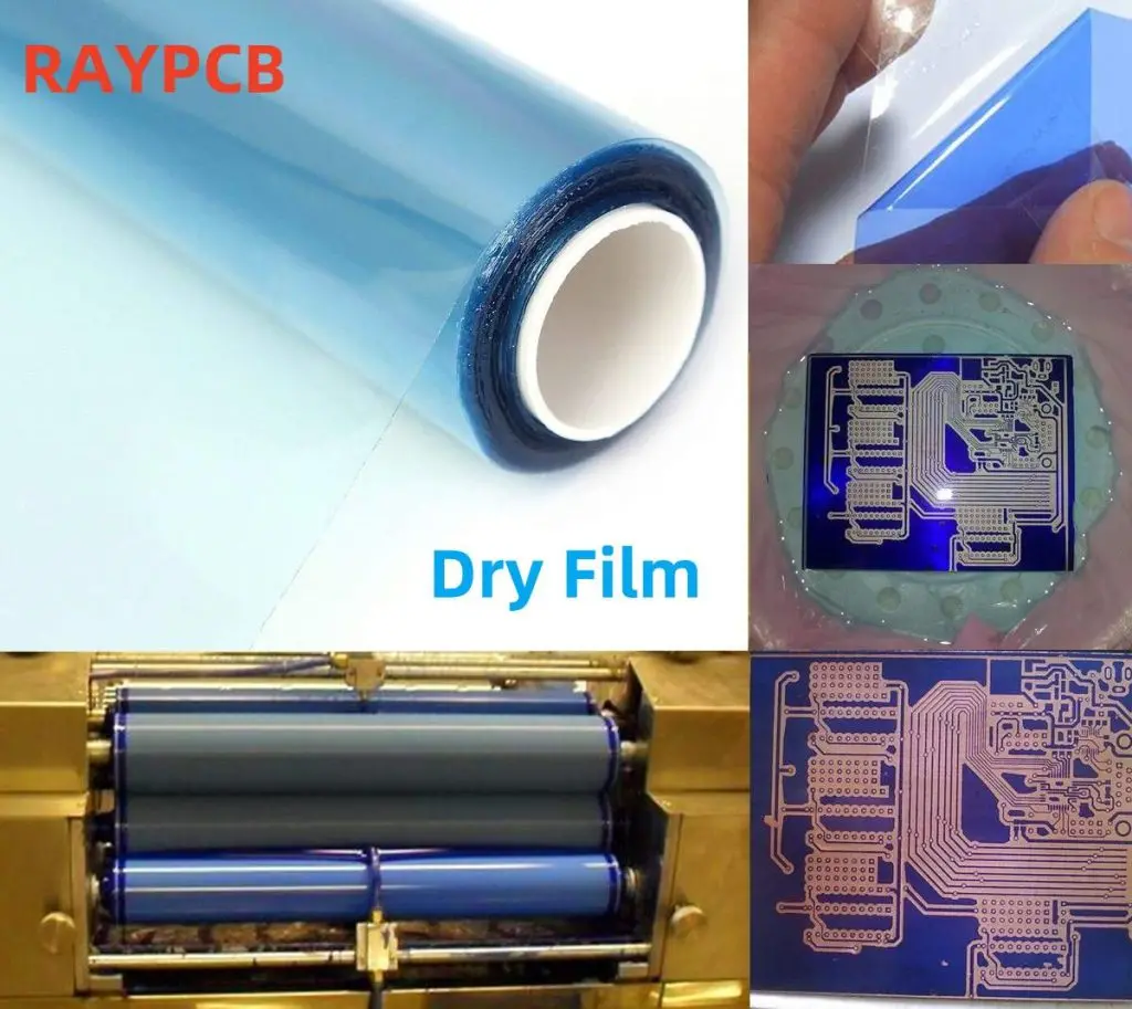
Defining Dry Film Photoresist
Dry film photoresist is a photosensitive material central to PCB production. It consists of a photopolymer layer sandwiched between two protective sheets. When exposed to ultraviolet (UV) light, the photoresist undergoes a chemical transformation, enabling precise pattern transfer onto the PCB substrate.
The Journey of Photoresist Technology
The evolution of photoresist technology in PCB manufacturing has been nothing short of remarkable. From the initial use of liquid photoresists to the development of dry film alternatives, this technology has continuously adapted to meet the escalating demands of the electronics industry.
The Liquid Photoresist Era
In the early days of PCB fabrication, liquid photoresists were the primary solution. While effective, they presented challenges in terms of uniformity and handling, particularly for high-volume production scenarios.

The Dry Film Photoresist Revolution
The introduction of dry film photoresist marked a turning point in PCB manufacturing. This innovation addressed many of the shortcomings of liquid photoresists, offering improved consistency, ease of use, and compatibility with automated processes.
Key Benefits of Dry Film Photoresist
Unparalleled Uniformity and Thickness Control
A primary advantage of dry film photoresist is its ability to provide exceptional uniformity across the PCB surface. This consistency is crucial for achieving precise circuit patterns, especially in high-density designs where every micron matters.
Superior Resolution and Edge Definition
Dry film photoresist enables sharper edge definition and higher resolution in circuit patterns. This capability is invaluable as PCBs become increasingly complex and compact, necessitating finer lines and spaces.
Streamlined Handling and Processing
The solid nature of dry film photoresist simplifies handling and application compared to liquid alternatives. It can be easily laminated onto PCB substrates, minimizing the risk of contamination and ensuring more comprehensive coverage.
Eco-friendly and Health-conscious
Dry film photoresist is generally considered more environmentally friendly than its liquid counterparts. It generates less waste and reduces exposure to potentially harmful chemicals during the application process, aligning with modern sustainability goals.
Read more about:
The Dry Film Photoresist Workflow in PCB Production
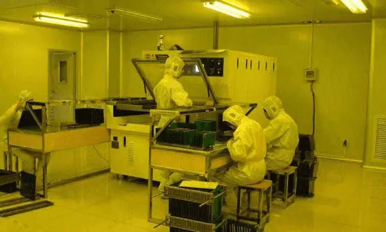
Phase 1: Surface Preparation and Cleaning
Before applying dry film photoresist, the PCB substrate undergoes thorough cleaning to ensure optimal adhesion. This crucial step typically involves mechanical or chemical cleaning processes to eliminate surface contaminants.
Phase 2: Lamination Process
The dry film photoresist is carefully laminated onto the PCB substrate using a combination of heat and pressure. This process ensures uniform coverage and strong adhesion to the board surface, setting the stage for subsequent steps.
Phase 3: UV Exposure
The laminated board is exposed to UV light through a photomask containing the desired circuit pattern. This exposure triggers polymerization in the exposed areas, creating a hardened image of the circuit design.
Phase 4: Development Stage
Following exposure, the board undergoes a development process. This step removes the unexposed photoresist, leaving behind the desired circuit pattern and preparing the board for etching.
Phase 5: Etching Process
With the protective photoresist pattern in place, the board is subjected to an etching process. This step removes the exposed copper, creating the final circuit pattern with precision.
Phase 6: Resist Stripping
Once etching is complete, the remaining photoresist is stripped away, revealing the finished circuit pattern on the PCB and concluding the core fabrication process.
Diverse Applications of Dry Film Photoresist in PCB Manufacturing

High-Density Interconnect (HDI) PCBs
Dry film photoresist plays a pivotal role in the production of HDI PCBs, which demand extremely fine lines and spaces. Its high resolution and excellent edge definition make it ideal for these cutting-edge applications.
Flexible PCB Solutions
The adaptability of dry film photoresist makes it well-suited for manufacturing flexible PCBs. These versatile boards are increasingly used in compact electronic devices and wearable technology, where flexibility is paramount.
Multilayer PCB Fabrication
In the production of multilayer PCBs, dry film photoresist is used to create precise patterns on each layer. Its consistency and reliability are essential for ensuring proper alignment and functionality across all layers of these complex boards.
Rigid-Flex PCB Integration
Rigid-flex PCBs, which combine rigid and flexible board technologies, benefit significantly from the versatility of dry film photoresist. It can be effectively applied to both rigid and flexible substrates, ensuring uniform circuit patterns throughout the hybrid board.
Navigating Challenges in Dry Film Photoresist Usage
Optimal Storage and Handling Practices
Dry film photoresist is sensitive to environmental factors such as light, temperature, and humidity. Implementing proper storage and handling procedures is crucial to maintain its quality and effectiveness throughout its shelf life.
Precision in Equipment and Process Control
Achieving optimal results with dry film photoresist requires precise control over various process parameters, including lamination temperature, exposure time, and development conditions. This level of control demands sophisticated equipment and well-trained operators.
Ensuring Substrate Compatibility
While dry film photoresist is versatile, ensuring compatibility with various PCB substrate materials can be challenging. Different substrates may require specific types of photoresist or modified processing conditions to achieve optimal results.
Application-Specific Optimization
Each PCB application may have unique requirements in terms of resolution, thickness, and other properties. Fine-tuning the dry film photoresist process to meet these specific needs can be complex and time-consuming, requiring expertise and patience.
Innovation Horizons in Dry Film Photoresist Technology
Next-Generation Photoresist Formulations
Ongoing research is focused on developing new photoresist formulations with improved properties, such as higher resolution, better adhesion, and enhanced resistance to harsh manufacturing conditions, pushing the boundaries of what’s possible in PCB fabrication.
Synergy with Additive Manufacturing
As additive manufacturing techniques gain traction in PCB production, dry film photoresist technology is evolving to support these new processes, offering potential for even more precise and efficient circuit creation in the era of 3D-printed electronics.
Eco-Innovation in Photoresist Solutions
The push for more sustainable manufacturing practices is driving the development of eco-friendly dry film photoresist options, with a focus on reducing environmental impact, improving recyclability, and minimizing the carbon footprint of PCB production.
Industry 4.0 Integration
The integration of dry film photoresist processes with advanced automation and Industry 4.0 technologies promises to enhance efficiency, reduce errors, and improve overall PCB manufacturing quality, ushering in a new era of smart manufacturing in the electronics industry.
Conclusion: The Enduring Significance of Dry Film Photoresist
As we’ve explored throughout this article, dry film photoresist stands as a cornerstone technology in the realm of PCB fabrication. Its capacity to deliver precision, consistency, and versatility makes it an indispensable tool in the electronics manufacturing industry.
From enabling the production of high-density interconnect boards to supporting the development of flexible and multilayer PCBs, dry film photoresist continues to push the envelope of possibility in circuit board design and manufacturing. Its ongoing evolution, driven by relentless research and innovation, ensures that it will remain at the forefront of PCB manufacturing technology for years to come.
As electronic devices become increasingly compact, complex, and ubiquitous, the role of dry film photoresist in PCB fabrication is set to grow even more critical. It stands as a testament to the ingenuity and continuous improvement that drives the electronics industry forward, playing a vital role in shaping the electronic landscape of tomorrow.
For PCB designers, manufacturers, and technology enthusiasts alike, understanding the role of dry film photoresist provides valuable insight into the precision and innovation that underpins our modern digital world. As we look to the future, it’s clear that this unassuming yet critical technology will continue to be a key player in the ongoing revolution of electronic design and manufacturing.