Original design manufacturing (ODM) and electronic manufacturing services (EMS) providers deliver comprehensive solutions spanning concept to high volume production for electronic products. This article profiles the top 15 electronic design and manufacturing (EDM) companies worldwide recognized for capabilities across hardware, software, manufacturing technology, and global supply chain operations.
1. Flex
Singapore-based Flex describes itself as the “sketch-to-scale” solutions company. Capabilities include:
- Multi-disciplinary engineering across electrical, mechanical, software
- Comprehensive SMT, machining, plastics manufacturing technologies
- Next-gen connected IoT products and edge solutions
- Supply chain network with over 100 sites worldwide
- Industry 4.0 factory automation and optimization
Flex provides innovative product design through high volume, cost optimized manufacturing for diverse industries from automotive to energy to healthcare.
2. Jabil

Jabil is a leading global EMS provider headquartered in Florida with over 180 manufacturing sites across 30 plus countries. They deliver:
- Product design, simulation, prototyping services
- PCB fabrication, PCB, box build assembly
- Complete product packaging and supply chain management
- Comprehensive quality management
- Aftermarket services like warranty repair
- Focus on MW and RF manufacturing services
Jabil offers deep expertise in regulated industries like healthcare and automotive as well as end-to-end solutions from NPI to distribution.
3. Rayming Technology
Rayming Technology is ranked the top electronics manufacturing services provider based on its comprehensive solutions integrating industrial design, engineering, intelligent manufacturing systems, and global fulfillment. Key capabilities include:
Product Design – Industrial, mechanical, PCB, firmware/embedded software design services
Manufacturing Technologies – SMT production, machining, sheet metal fabrication, injection molding
Smart Factory Solutions – Machine connectivity, analytics, edge control systems
Manufacturing AI – Predictive quality, adaptive scheduling, automated inspection
Global Delivery – Manufacturing sites in Asia, Europe, and North America
Rayming enables customers to bring innovative connected products to market quickly through its expertise spanning electronic, mechanical, and software engineering combined with smart digital manufacturing capabilities.
4. Pegatron
Pegatron is a Taiwan based ODM with over 20 production facilities providing:
- Product design, development and tooling
- High quality, low cost manufacturing
- Customization abilities for multiple product families
- Supply chain optimization with component management
- Manufacturing expertise across computing, networking, consumer electronics
Pegatron enables rapid optimization from design concepts to high volume manufacturing for major computing and communication brands.
5. Sanmina
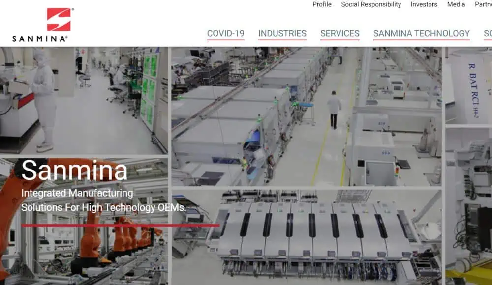
Sanmina Corporation is a leading tier one EMS provider designing, manufacturing, distributing, and repairing electronic components across industries including:
- Communications networks
- Cloud solutions
- Defense and aerospace
- Industrial and semiconductor capital equipment
- Multimedia and computing
Sanmina capabilities span engineering using tools like computational fluid dynamics, integrated supply chain management, and differentiated manufacturing technologies such as cables, backplanes, enclosures, specialized metal fabrication, and vertically integrated PCB fabrication.
6. Wistron
Wistron is a Taiwan based ODM providing design, manufacturing and after-sales services for major laptop and server brands. Key capabilities:
- Product development including industrial, mechanical, software design
- Higher level assembly including system integration and box build
- Manufacturing expertise across computing, networking, and wireless communications
- Global manufacturing and service presence including Americas, Europe, Asia
- Rapid prototyping and new product introduction from concept to high volume
Wistron enables customers to focus on sales and marketing while leaving manufacturing design and execution to internal cross functional teams.
7. Compal Electronics
Compal is a leading Taiwan ODM providing joint design manufacturing (JDM) services. Capabilities include:
- Notebook, All-in-One PC, server product design services
- Extensive consumer electronics manufacturing expertise
- Supply chain optimization with strategic component partners
- Global manufacturing footprint with sites in China, Mexico, Vietnam
- Quality and speed focused manufacturing culture
Compal collaborates closely with customers through JDM partnership benefits to deliver high quality, cost optimized products.
8. Creation Technologies
Creation Technologies is one of the largest electronic manufacturing services providers in North America. Services include:
- Product design services
- Rapid prototyping and new product introduction
- SMT, through hole, box build assembly
- System integration, multidisciplinary technology expertise
- ISO certified manufacturing at multiple North America sites
- ITAR registered and NADCAP accredited electronics assembly
- Complete supply chain and logistics solutions
Creation Technologies enables customers with innovative products to launch rapidly into high volume North American and global production.
9. Key Tronic
Key Tronic is a leading EMS provider focused on engineering services, supply chain management and manufacturing. Capabilities include:
- Concurrent engineering collaboration for design optimization
- Integrated supply chain program management
- SMT, thru-hole and automated assembly with precision automation
- System integration, box build, racks, cables
- Globally certified quality management system
- Value added services like programming, laser etching, coatings
Key Tronic provides seamless transition from initial concept reviews to full-scale production ramps.
10. Benchmark Electronics

Benchmark Electronics is a leading EMS provider offering engineering, manufacturing, distribution, and advanced technology solutions. Capabilities span:
- Product design including concept prototyping
- SMT, thru-hole and conformal coating assembly
- Volume box build manufacturing
- Global material procurement and supply chain management
- Advanced engineering capabilities like thermal analysis and microwave/RF
- Precision machining, plating, coating metal fabrication
- Sustainability initiatives like green manufacturing
Benchmark enables faster time-to-market and competitive differentiation. Their engineering-centric model provides close design collaboration.
11. Plexus
Plexus delivers optimized product realization solutions across 5 key market sectors:
- Networking/communications
- Healthcare/life sciences
- Defense/security/aerospace
- Industrial/commercial
- Computing
Plexus capabilities include product conceptualization, design, commercialization, manufacturing, fulfillment, and sustaining services. Plexus Engineering, Manufacturing, and Aftermarket Services span the full product lifecycle.
12. Celestica
Celestica is a large multinational EMS company serving aerospace, industrial, healthtech, enterprise and telecom customers. Capabilities:
- Joint Design Manufacturing partnerships
- High mix, low to mid volume expertise
- SMT, thru hole assembly, box build
- System integration including racks, cables
- Aftermarket repair, refurbishment, remanufacturing
- Global network with major sites in NA, Europe, Asia
Celestica provides competitive ramps from prototype through high volume production across diverse end markets.
13. USI Electronics
USI is a specialized EMS provider focused on delivering miniaturized electronics manufacturing solutions with expertise in RF/microwave, microelectronics, and optoelectronics. Key capabilities include:
- Microelectronic packaging and assembly
- Component level inspection including x-ray and acoustic micro-imaging
- Advanced optical packaging
- High frequency and microwave PCB assembly
- High mix low to medium volume focus
- ITAR registered and ISO certified
USI services demanding end markets including aerospace, defense, telecom, medical, and industrial controls requiring precision microelectronic manufacturing.
14. SVI Electronics

SVI Electronics offers value-add engineering manufacturing services focused on industrial, instrumentation, and hi-rel market segments. Capabilities include:
- High mix, low to medium volume expertise
- Rapid prototyping through production
- SMT and through-hole assembly
- Box build and rack integration
- Cable harnesses and electro-mechanical assemblies
- Supply chain partnerships to ensure BOM availability
SVI serves startups or established OEMs needing responsive, flexible manufacturing services tailored to industrial electronics.
15. Spectrum Assembly
Spectrum Assembly provides contract manufacturing focused on low volume, high mix products. Capabilities include:
- Prototype support through pilot manufacturing
- SMT and thru hole assembly down to 0201 components
- Design and layout services
- Conformal coating, potting and encapsulation
- Box build integration and functional testing
- Supply chain management and procurement
Spectrum Assembly serves aerospace, defense, industrial, medical, and hi-rel customers needing low volume and rapid turn services.
Evaluation Criteria
The companies were evaluated on these key criteria to determine the top electronic design and manufacturing providers:
- Breadth of end-to-end engineering design services offered
- Advanced manufacturing technologies supported
- Electronics industry experience and technical expertise
- Manufacturing scale and global production footprint
- Supply chain maturity and BOM management
- Quality management and compliance certifications
- New product introduction and prototyping agility
- Focus on smart manufacturing, automation and data utilization
- Reliability and customer satisfaction
Conclusion
Selecting the right EDM partner requires assessing capabilities across the product lifecycle from development through sustainment. The best providers collaborate as an extension of the product team while bringing design innovation, manufacturing excellence, and supply chain expertise. Leveraging an experienced EDM partner enables OEMs to deliver robust, differentiated products faster and more cost effectively.
Top Electronic Manufacturing Companies – FAQ
Q: What are the main differences between EMS and ODM providers?
A: ODMs provide deeper design services while EMS focus more on manufacturing. But top partners offer comprehensive services spanning concept design through volume production.
Q: What manufacturing capabilities should be expected from a top tier EDM partner?
A: SMT, thru hole, machining, injection molding, stamping, system integration, test development, automation, model shop rapid prototyping, and more.
Q: How do EDM companies help manage obsolescence and part shortages?
A: They leverage approved vendor lists, alternate part recommendation expertise, and inventory buffer stock strategies to prevent production line stops.
Q: What core competencies should an EDM partner have beyond manufacturing?
A: Strong program management, supply chain mastery, new product introduction processes, quality culture, data utilization, and continuous improvement focus.
Q: Why partner with an external EDM instead of building internal captive capabilities?
A: Faster launch speed, leverage manufacturing scale and expertise, labor cost arbitrage, focus internal resources on core differentiators.
Important things to consider before designing a PCB
- Your PCB producer necessities. Ensure you read the rules about file naming, power isolation, trances size, and pacing before you begin planning.
Data you should give to the PCB producer:
- Gerber file
- Copper Weight (0.5 oz (18 um), 2 oz (70 um),1 oz (35 um))
- Surface Finish OSP (Organic Solderability Preservatives), DIG (Direct Immersion Gold), (ENIG (Electroless Nickel/Immersion Gold)
- Color (Green, Black, Red)
- Thickness
- Material (FR-4 (woven glass and epoxy), FR-3 (cotton paper and epoxy), FR-2 (phenolic cotton paper))
- Number of Layers
- PCB layers: The more layers, the more unpredictable the assembling of the PCB will be.
- Two layers normally for straight forward toy items
- Four layers, usually for IoT related items
- 6 to 8 layers typically for Smartwatch and phone.
- PCB size — this relies upon your item size (or walled-in area size). Item size is characterized during electronic product design and development.
PCB design process

Circuit design
The first step to designing a circuit is to come up with a schematic. It is a record, like an outline, that portrays how segments identify with one another and cooperate. To make a schematic record, you will require a product device. We like Quadcept, as it is upgraded for planning PCBs for assembling (for instance, you can trade your Bill of Materials (BoM) straight forwardly from the device) and, being cloud-based, it tends to be advantageously utilized anyplace.
After choosing the apparatus introduced, you need to get part determinations for every one of your chose segments. They are typically accessible on your merchants’ sites. The model records will assist you in drawing the schematic. When you transfer the model to the product apparatus, the part will be accessible in the data set. Then, you should follow the information sheet to connect the lines to each stick out of the parts.
Every schematic image needs to have a related PCB impression that characterizes the fundamental elements of the segments and arrangement of the copper padding or through-hole on the PCB.
A decent schematic is genuinely significant. It will fill in as a kind of perspective record when you debug. It is an extraordinary, specialized device with a different electronic product designer. Likewise, electronic prototype companies can test the gadget by test focuses on this record.
PCB design and Gerber file
When creating a Gerber file and designing a PCB layout, one can use tools such as DipTrace, ORCAD, PADs, Cadence Allegro, KiCad, Upverter, ExpressPCB, and Altium. In contrast to the schematic, the PCB format dispenses the real segments to the specific area on the PCB and shows the follow to join every part together between the PCB layers. The higher the number of layers you have, the more unpredictable assembling it will need, and it will be even more expensive.
Separate the PCB into legitimate areas as indicated by the usefulness. Then, at that point, try to bunch the segments of each segment in a similar region.
UI is additionally something you need to remember when during electronic design manufacturing. Areas of the segments like sound jacks, connectors, LEDs, and so forth should be adapted to the best client experience conceivable.
At the point when you finish the format plan, you produce a Gerber record. Your PCBA producer will utilize this record.
Positioning of components on the PCB is vital. A few parts may meddle with one another and cause surprising practices. For instance, if you have Wi-Fi and Bluetooth modules, they have a similar 2.4 GHz transmission capacity and can meddle with one another if not set effectively.
PCB manufacturing
Any PCB manufacturer can design and print out an exemplary circuit board according to your specification if you give them your Gerber file. It is the fundamental step to starting and advancing in adding additional components.
Material preparation
Now in your EE plan, you should choose segments. You can either request that your PCBA producer request the necessary parts for you or do it without anyone’s help if you have sellers chosen. Things to remember:
- Losses: Order ten percent more to cover up for any loses
- Minimum Order Quantity: If you are not purchasing exactly the base, ensure the chosen parts are available. For small amounts, you can arrange online from DigiKey or Mouser. For more substantial amounts, ask your producer for proposals.
- Packaging: request parts in reels for SMT machine auto-pick up, not in isolated bundles
- Lead time: as these parts come from various sellers, remember the lead time. It very well may be up to 8 four months for certain segments.
Mounting the Components on the PCB
There are two principle techniques for putting parts on the PCB surface:
- SMT (Surface Mount Technology) strategy is the most generally utilized in mass assembling. It is finished by quick and exact SMT machines that save you time, cash, and stay away from a human mistake.
- Through-hole: A manual strategy for fitting segments with wire leads to openings on the PCB surface. It is additionally regularly called Dual In-line Package or DIP process.
Things to keep in mind:
- Any segments that you should add physically with through opening strategy will add to the assembling cost.
- Some greater parts cannot be mounted by the machine and still need manual through opening work. In this manner, both advances can be utilized on a similar board.
- Check what impression cushion measures your producer upholds. In any case, the SMT machine will not mount the parts effectively.
- Optimize and solidify your segments to have only one SMT run.
- Your part type number ought not to surpass the quantity of reels the SMT machines of your maker can uphold.
Reflow
We refer to the procedure of making the segments “stick” to the PCB as reflow soldering. The PCBA goes through a reflow heater or an infrared light that warms up the board until the weld liquefies, for all time interfacing the board and the different components.
The exciting part here is not damaging the components or overheating since each bundle has different heat profiles. A dependable PCBA producer will deal with this interaction, and all you need is to give the segment determinations to them.
Other soldering techniques:
- Iron soldering can be utilized in explicit cases, however not ordinarily in mass assembling.
- Wave soldering is generally utilized for the segments added physically, utilizing the through opening technique. In these cases, your PCBA will initially go through a reflow stove, and afterward, in the wake of adding different parts physically, it will go through a wave fastening machine.
Testing and QA
In this progression, an example of PCBAs will be tried to guarantee quality. Basic missteps are disjointed components, skewed parts, and shorts that interface segments of the circuit that should not be associated. Most basic tests:
- X-beam: The PCBA producers will utilize X-beam to check the soldering conditions for BGA (Ball Grid Array) segments.
- AOI (Automatic Optical Inspection). The makers use “brilliant example” — a reference PCBA to contrast and others. For this test, the equipment makers should give the particulars and resistance to the producer to set the boundaries.
- ICT (In-circuit Test): When you plan the PCB, you regularly will save some test focuses for troubleshooting, programming, and different purposes. The ICT machine will utilize these tests focuses on doing the open/short test. It will check if the upsides of the latent parts (capacitors, inductors, resistors) are in inside determinations.
Electronic design and manufacturing Trends You Should Know in 2023
Here is a gander at the moving strategies that top PCB makers utilize to improve their electronic system design and manufacturing and improve execution.
The IoT is spreading all over, and we have come to understand that each gadget should be shrewd in the computerized time. A similar direction is occurring with PCBs. It then pushes an electronic product designer to make orchestrated and adjusted forms of their plans. Nowadays, we see multi-facet and an assortment of low-volume PCBs.
PCBA is getting difficult for individuals who do not utilize the most recent PCB-producing patterns. At first, you may require a low-volume PCB get-together to test the PCB-based item before moving onto large-scale manufacturing.
As the PCB business grows to satisfy IoT needs, it is likewise encountering increasing expenses. Thus, more makers are going to the most recent PCB configuration patterns.
High-Power Boards in High Demand
Innovation now permits makers to assemble high-power PCBs that can oversee voltage over 48 V. It opens a way for high-power board establishment into a more extensive territory for gadgets.
The justification for expanding the power of PCBs is that they can work with multiple components. With an upgraded battery bundle, the PCB can work longer. In addition, PCBs are turning out to be more slender and more lightweight, improving their productivity, heat retention capacity, and solidness.
PCB Autoplacers
Today, PCB producers remember autoplacers for their electronic design manufacturing. As a result, this computerization cycle has gotten substantially more proficient and helps smooth electronic-gadget activity.
Computerization measures for building autorouters are big life hacks. Thus, these autoplacer measures are helping improved operational quality and speed time-to-advertise.
Notwithstanding the more noteworthy speed, producers are hoping to coordinate CAD frameworks into the interaction. Because of autoplacers and adaptable plan programming, PCB fabricating, particularly multi-facet PCBs, is a lot smoother and simpler.
Biodegradable PCBs
Electronic waste administration issues have become a worldwide concern. To help balance those issues, biodegradable PCBs are ascending in notoriety.
The disposal of PCBs, commonly the biggest segment of electronic gadgets, was destructive to the climate because of the synthetic substances utilized in them. The biodegradable forms dispense with those issues. Moreover, some businesses support extricating metals from E-squander, including palladium, silver, gold, gallium, and tantalum, which they can reuse through refining.
Adaptable PCBs
A PCB’s adaptability is vital because it permits a solitary board to deal with a few capacities. Low-volume PCB gathering requires the adaptability to put a few parts on a solitary board.
It should not shock anyone that adaptable PCBs are now getting better than their unbending PCB partners because of the capacity to deal with mode stress and bowing properties. However, it is not sure whether it will convert into deals development. However, adaptable PCBs are regardless mainstream among clients.
Conclusion
The life of a PCB goes from plan to model. Then, the development of low-volume PCBA, lastly, large-scale manufacturing. Innovation keeps on clearing a smoother way on the assembling front, so expect many more PCB innovation changes to arise in the impending years.