In the ever-evolving world of electronics, flexible printed circuit boards (PCBs) have become increasingly popular due to their versatility and ability to fit into compact spaces. Among these, 6 layer flexible PCBs stand out as a powerful solution for complex electronic designs. This article delves into the intricacies of 6 layer flexible PCBs, covering their design, manufacturing process, cost considerations, and applications.

What is 6 Layer Flexible PCB?
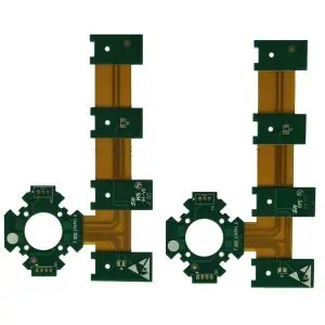
A 6 layer flexible PCB is an advanced type of flexible circuit board that consists of six conductive layers separated by insulating materials. These boards combine the flexibility of thin, pliable substrates with the complexity and functionality of multi-layer PCBs.
Key Features of 6 Layer Flexible PCBs:
- Flexibility: Can bend, fold, or flex without damaging the circuitry
- Complexity: Allows for intricate circuit designs with high component density
- Thin profile: Despite having six layers, these PCBs maintain a relatively thin profile
- Durability: Resistant to vibration and movement, ideal for dynamic applications
- Weight reduction: Lighter than traditional rigid PCBs of similar complexity
Learn more about:
6 Layer Flex PCB Stackup

The stackup of a 6 layer flexible PCB is crucial to its performance and manufacturability. A typical stackup might look like this:
- Top layer: Flexible copper foil
- Insulating layer: Polyimide or other flexible dielectric
- Inner layer 1: Copper
- Core: Flexible dielectric material
- Inner layer 2: Copper
- Insulating layer: Polyimide or other flexible dielectric
- Inner layer 3: Copper
- Core: Flexible dielectric material
- Inner layer 4: Copper
- Insulating layer: Polyimide or other flexible dielectric
- Bottom layer: Flexible copper foil
Considerations for Stackup Design:
- Signal integrity: Proper placement of ground and power planes
- Impedance control: Careful management of trace widths and dielectric thicknesses
- Flexibility requirements: Balancing the need for flexibility with electrical performance
- Thermal management: Incorporating thermal dissipation strategies in the stackup
How to Design 6 Layer Flexible PCB
Designing a 6 layer flexible PCB requires careful planning and consideration of various factors:
1. Define Requirements
- Determine the circuit’s electrical requirements
- Establish mechanical constraints (bend radius, flex cycles)
- Identify environmental factors (temperature, humidity, chemical exposure)
2. Choose Materials
- Select appropriate flexible substrate materials (e.g., polyimide, LCP)
- Determine copper weight for each layer
- Choose adhesives and coverlay materials
3. Create Schematic
- Develop a comprehensive circuit schematic
- Organize components logically for optimal layer usage
4. Plan Layer Stack
- Decide on layer allocation (signal, power, ground)
- Ensure proper shielding and signal integrity
5. Component Placement
- Place components strategically, considering flex zones
- Minimize stress on solder joints in flex areas
6. Routing
- Route traces with flexibility in mind
- Use curved traces in flex zones to reduce stress
- Implement impedance control for high-speed signals
7. Design Rules and Checks
- Set up design rules specific to flexible PCBs
- Perform thorough design rule checks (DRC)
8. Documentation
- Create detailed fabrication and assembly drawings
- Specify bend lines, stiffener locations, and special instructions
Cost Estimate of 6 Layer Flexible PCB

The cost of 6 layer flexible PCBs can vary significantly based on several factors:
Factors Influencing Cost:
- Materials: High-performance flexible substrates can be costly
- Size: Larger boards generally cost more
- Complexity: Intricate designs with fine traces increase manufacturing costs
- Volume: Higher quantities typically reduce per-unit costs
- Turnaround time: Rush orders often incur additional fees
Approximate Cost Ranges:
- Prototyping: 500−500−2000 per board
- Small production runs (50-100 units): 200−200−500 per board
- Large production runs (1000+ units): 50−50−200 per board
These figures are rough estimates and can vary significantly based on specific requirements and manufacturers.
Cost Reduction Strategies:
- Optimize design for manufacturability
- Consider panel utilization to reduce material waste
- Explore alternative materials that meet performance requirements
- Consolidate multiple rigid-flex boards into a single 6 layer flex design
How is 6 Layer Flexible PCB Manufactured
The manufacturing process for 6 layer flexible PCBs involves several intricate steps:
1. Material Preparation
- Cut flexible copper-clad laminates to size
- Clean and prepare surfaces
2. Inner Layer Processing
- Print circuit patterns on inner layers
- Etch copper to create traces and pads
- Inspect and clean inner layers
3. Lamination
- Stack inner layers with prepreg and bonding materials
- Apply heat and pressure to fuse layers together
4. Drilling
- Drill holes for vias and component mounting
- Plasma clean holes to ensure good copper adhesion
5. Plating
- Electroless copper plating to coat hole walls
- Electrolytic copper plating to build up copper thickness
6. Outer Layer Imaging
- Apply photoresist to outer layers
- Expose and develop circuit patterns
7. Etching and Stripping
- Etch exposed copper to create final circuit pattern
- Strip remaining photoresist
8. Solder Mask and Surface Finish
- Apply solder mask to protect circuits
- Add surface finish (e.g., ENIG, immersion tin)
9. Coverlay Application
- Apply coverlay material to protect outer layers
- Cure coverlay using heat and pressure
10. Profiling and Cutting
- Cut board to final shape
- Create flex zones if required
11. Electrical Testing
- Perform automated electrical testing to ensure connectivity
12. Final Inspection and Packaging
- Visually inspect boards for defects
- Package for shipping or assembly
Applications of 6 Layer Flexible PCB
6 layer flexible PCBs find use in a wide range of applications due to their unique combination of flexibility and complexity:
Consumer Electronics
- Smartphones and tablets
- Wearable devices (smartwatches, fitness trackers)
- Digital cameras and camcorders
Medical Devices
- Implantable medical devices
- Hearing aids
- Portable diagnostic equipment
Automotive Industry
- In-vehicle entertainment systems
- Advanced driver-assistance systems (ADAS)
- Engine control modules
Aerospace and Defense
- Satellite components
- Radar systems
- Missile guidance systems
Industrial Applications
- Robotics and automation equipment
- Handheld testing devices
- IoT sensors and devices
Telecommunications
- 5G infrastructure equipment
- Optical networking devices
- High-speed data transmission systems
The versatility of 6 layer flexible PCBs makes them ideal for applications where space is limited, weight is a concern, or dynamic flexing is required. As technology continues to advance and miniaturize, the demand for these sophisticated flexible circuits is likely to grow across various industries.
In conclusion, 6 layer flexible PCBs represent a cutting-edge solution in the world of electronic design. While they present unique challenges in terms of design and manufacturing, their benefits in terms of flexibility, complexity, and space-saving make them an invaluable option for many modern electronic applications. As designers and engineers continue to push the boundaries of what’s possible in electronics, 6 layer flexible PCBs will undoubtedly play a crucial role in shaping the future of technology.