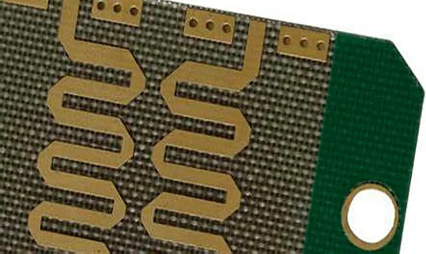
ENIG (Electroless nickel immersion gold) is a dual-layer metallic coating consisting of a thin gold layer deposited over an underlying nickel layer.
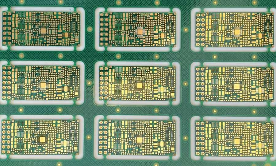
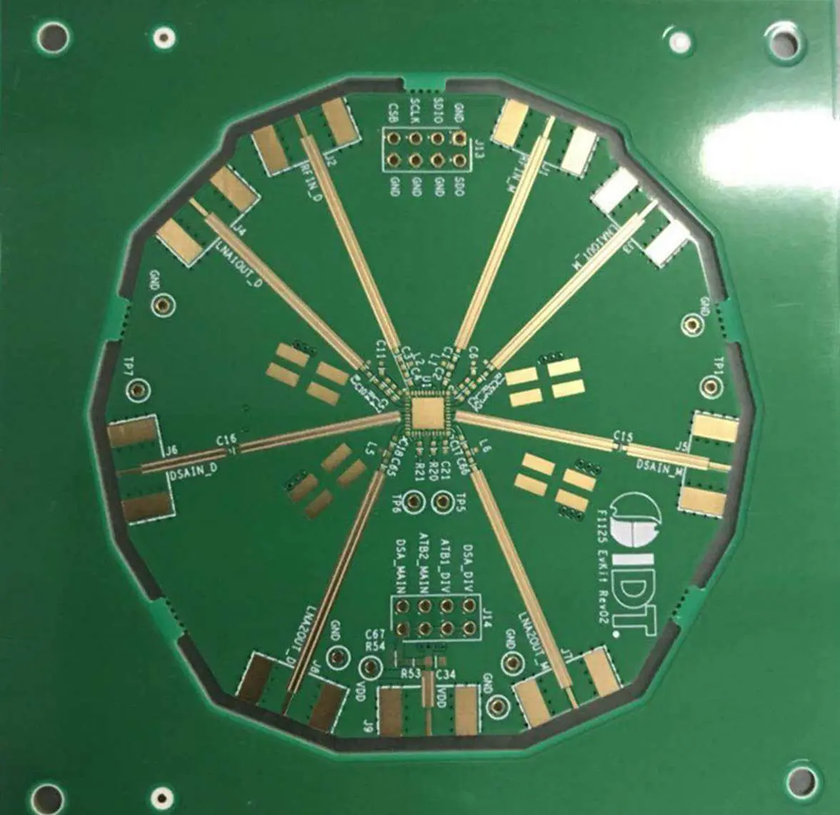
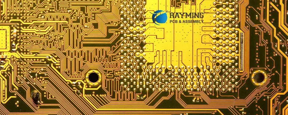
Printed circuit boards (PCBs) require surface finishes that provide excellent solderability, corrosion resistance, and long-term reliability. Among the various surface finish options available, Electroless Nickel Immersion Gold (ENIG) has emerged as one of the most popular and versatile choices for modern PCB applications. This comprehensive guide explores everything you need to know about ENIG PCBs, from their fundamental principles to practical applications and manufacturing considerations.
ENIG represents a sophisticated surface finishing technology that combines the protective properties of nickel with the superior conductivity and oxidation resistance of gold. This dual-layer approach has revolutionized PCB manufacturing, enabling the production of highly reliable electronic devices across industries ranging from consumer electronics to aerospace applications.
ENIG stands for Electroless Nickel Immersion Gold, a surface finish applied to printed circuit boards to protect copper traces and provide excellent solderability. Unlike traditional electroplating processes that require electrical current, ENIG utilizes chemical reactions to deposit both nickel and gold layers onto copper surfaces.
The ENIG finish consists of two distinct metallic layers:
This combination creates a robust, reliable surface that maintains its properties over extended periods, making it ideal for high-performance electronic applications.


The ENIG process involves several carefully controlled chemical steps that must be executed with precision to achieve optimal results:
1. Substrate Preparation The PCB substrate undergoes thorough cleaning to remove any contamination, oxidation, or residues that could interfere with the plating process. This typically involves:
2. Electroless Nickel Deposition The cleaned PCB is immersed in an electroless nickel plating solution containing:
The chemical reaction deposits a uniform nickel-phosphorus alloy layer across all exposed copper surfaces, regardless of geometry complexity.
3. Immersion Gold Deposition Following nickel deposition, the PCB enters an immersion gold bath where:
4. Final Processing The finished PCBs undergo final cleaning and inspection to ensure quality standards are met.
The electroless nickel deposition follows this primary reaction:
Ni²⁺ + H₂PO₂⁻ + H₂O → Ni + H₂PO₃⁻ + 2H⁺The immersion gold process involves:
Ni + 2Au³⁺ → Ni²⁺ + 2AuNickel Layer Characteristics:
Gold Layer Characteristics:
The interface between nickel and gold forms through a controlled displacement reaction that creates excellent adhesion. The thin gold layer allows for effective solder wetting while the nickel barrier prevents copper migration and maintains long-term reliability.
Temperature Control:
pH Management:
Solution Maintenance:
Thickness Monitoring:
Surface Analysis:
ENIG provides excellent solderability characteristics that remain stable over extended periods:
The dual-layer structure provides comprehensive protection:
ENIG’s electroless and immersion processes ensure consistent coverage:
ENIG offers superior electrical characteristics:
ENIG is generally more expensive than basic surface finishes:
Black Pad Defect:
Phosphorus Content Issues:
Thickness Variations:
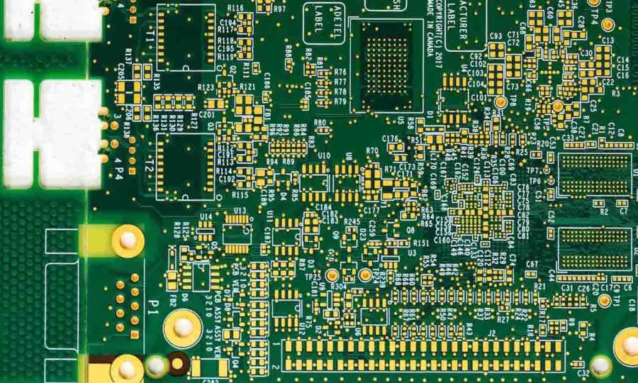
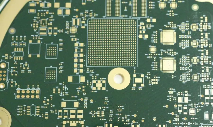
ENIG is widely used in consumer electronic devices:
The automotive industry relies heavily on ENIG for critical applications:
ENIG meets the stringent requirements of industrial and medical electronics:
Modern communication infrastructure depends on ENIG technology:

Advantages of ENIG:
Advantages of HASL:
Advantages of ENIG:
Advantages of OSP:
Advantages of ENIG:
Advantages of Immersion Silver:
Size Recommendations:
Shape Optimization:
Spacing Requirements:
Signal Integrity:
Substrate Compatibility:
Visual Examination:
Dimensional Verification:
In-Process Controls:
Statistical Process Control:
Solderability Testing:
Reliability Assessment:
Symptoms:
Causes:
Prevention:
Common Problems:
Solutions:
Sources of Contamination:
Prevention Strategies:
Equipment Costs:
Operating Expenses:
Process Efficiency:
Quality Improvements:
Chemical Waste Streams:
Environmental Compliance:
Resource Conservation:
Green Alternatives:
Process Improvements:
New Applications:
Industry Demands:
Emerging Technologies:
ENIG (Electroless Nickel Immersion Gold) represents a mature and versatile surface finishing technology that continues to play a crucial role in modern PCB manufacturing. Its combination of excellent solderability, superior corrosion resistance, and reliable performance makes it the preferred choice for demanding electronic applications across multiple industries.
While ENIG does present certain challenges, including higher costs and potential process complexities, the benefits far outweigh the disadvantages for applications requiring high reliability and long-term performance. The key to successful ENIG implementation lies in understanding the process fundamentals, maintaining proper quality control, and working with experienced suppliers who can provide consistent, high-quality results.
As the electronics industry continues to evolve toward smaller, more complex, and higher-performance devices, ENIG technology will likely remain a cornerstone of advanced PCB manufacturing. Ongoing developments in process chemistry, equipment design, and quality control methods will further enhance its capabilities and expand its applications.
For engineers and manufacturers considering ENIG for their PCB applications, careful evaluation of requirements, costs, and benefits will ensure optimal results. The investment in ENIG technology often pays dividends through improved product reliability, reduced field failures, and enhanced customer satisfaction.
The future of ENIG looks promising, with continued innovations addressing current limitations while expanding into new application areas. As environmental regulations become more stringent and sustainability concerns grow, the industry will likely see developments in more environmentally friendly chemistries and processes that maintain the excellent performance characteristics that make ENIG such a valuable surface finishing option.
Understanding ENIG PCB technology is essential for anyone involved in modern electronics design and manufacturing. This comprehensive guide provides the foundation for making informed decisions about surface finish selection and implementation, ensuring successful outcomes in today’s competitive electronics marketplace.