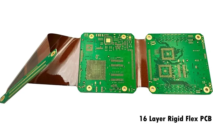
RayMing is a UL-certified rigid-flex PCB manufacturer specializing in high-layer-count solutions, with capabilities extending to 32-layer rigid boards and 6-layer flexible circuits. Contact us for competitive pricing quotes.
The global rigid flex PCB market is experiencing unprecedented growth, with industry analysts projecting a compound annual growth rate (CAGR) of 11.70%, reaching $77.7 billion by 2034. This explosive growth is driven by increasing demand in automotive, aerospace, consumer electronics, medical devices, and IoT applications. As electronic devices become more compact, intelligent, and versatile, rigid flex PCBs have emerged as the solution that combines the stability of rigid boards with the adaptability of flexible circuits.
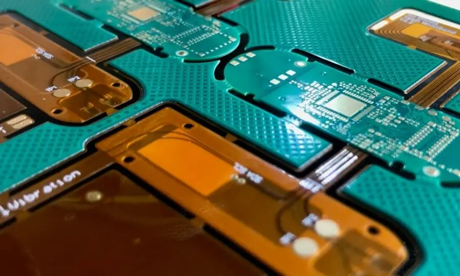
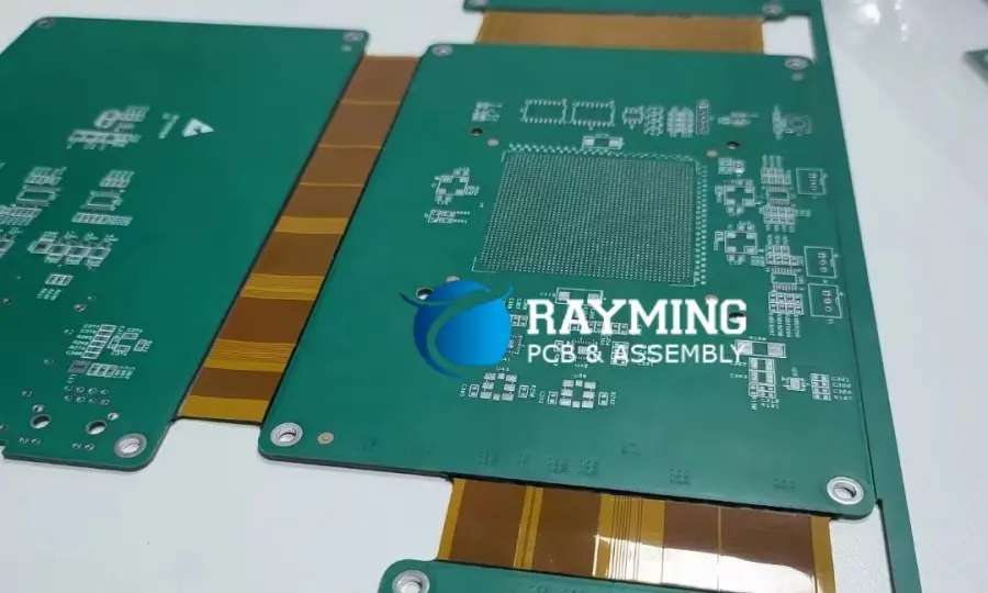
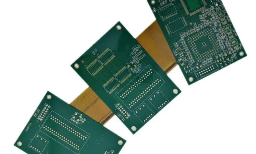
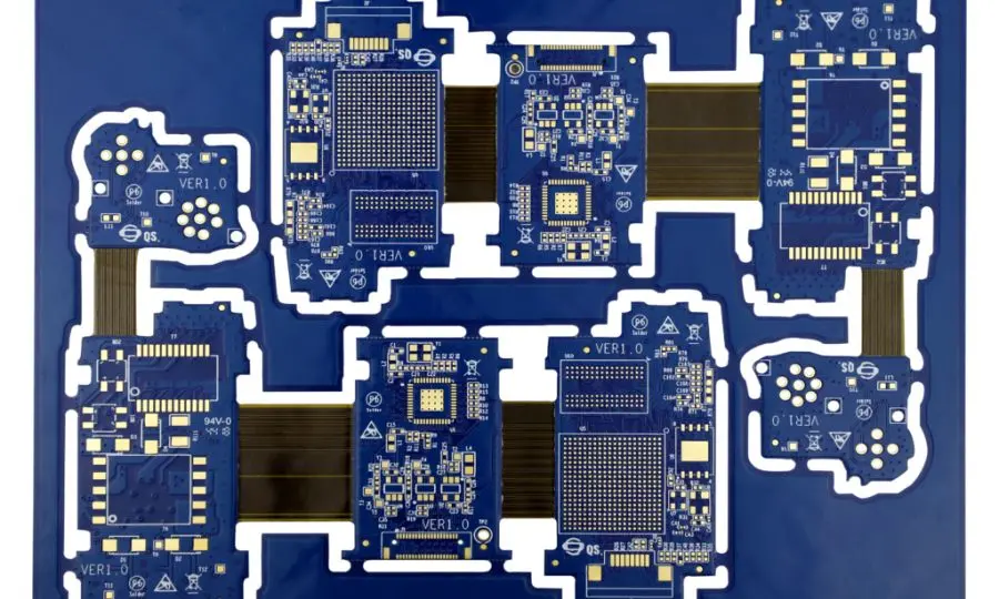
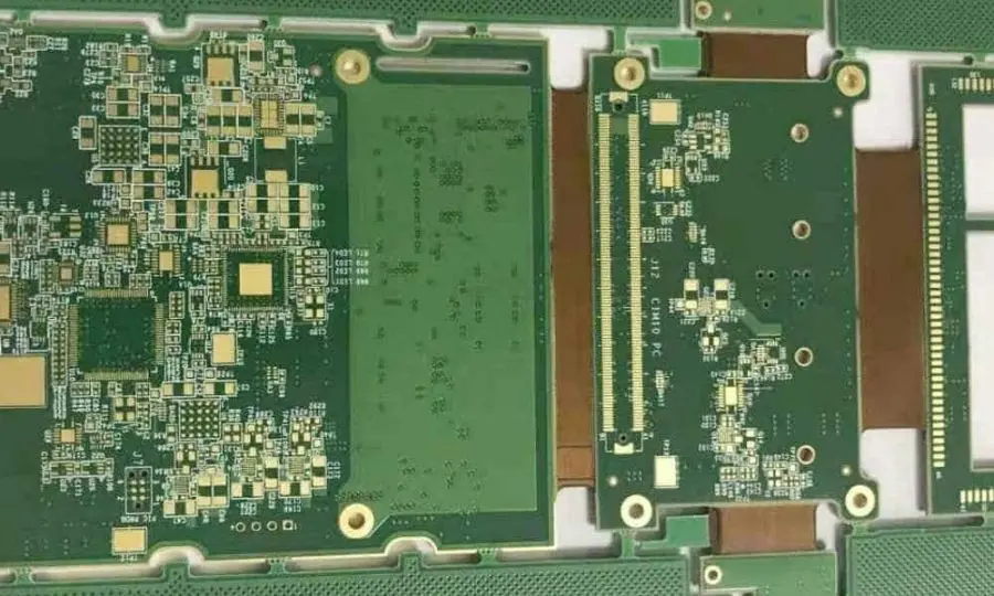
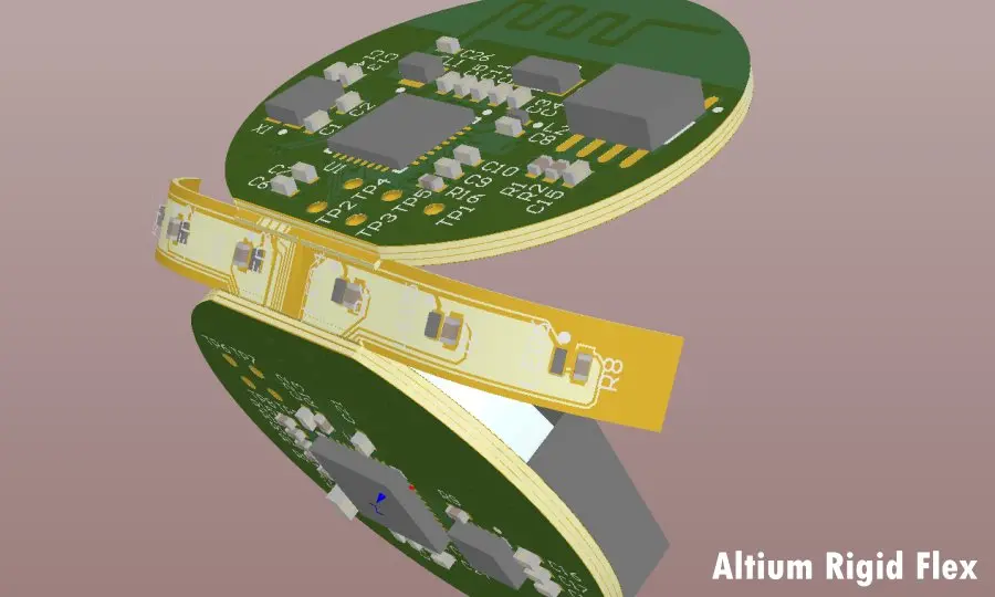
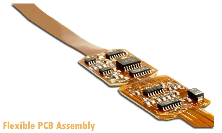
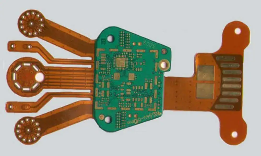
A rigid flex PCB is a sophisticated printed circuit board that integrates both rigid and flexible circuit sections into a single, unified assembly. Unlike traditional rigid PCBs that use only solid FR-4 material, or flexible PCBs made entirely of bendable polyimide, rigid flex boards strategically combine both technologies to create three-dimensional electronic solutions.
Rigid Sections:
Flexible Sections:
Transition Zones:
1. Single-Sided Rigid Flex (Type 1)
2. Double-Sided Rigid Flex (Type 2)
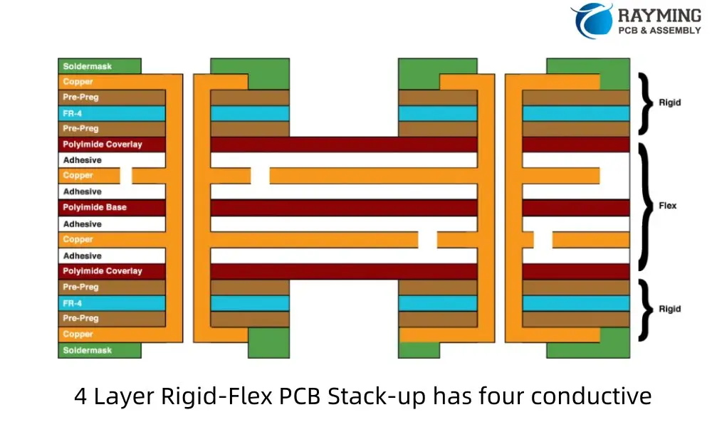
3. Multi-Layer Rigid Flex (Type 3)
4. Complex Multi-Layer (Type 4)
For dynamic flex applications (repeated bending), use adhesiveless constructions and Pyralux AP. For static flex (bend-to-install), standard acrylic adhesive systems are cost-effective. High-frequency designs benefit from LCP or Rogers materials with low Dk/Df values.
• Route traces perpendicular to the bend axis when possible
• Avoid vias in dynamic flex zones
• Use hatched polygons instead of solid copper planes
• Increase trace width in flex areas to reduce stress concentration
• Add teardrops at pad-to-trace transitions
Impedance is within ±10% of 50Ω target. Good for general RF applications.
| Application | Single-Ended | Differential | Notes |
|---|---|---|---|
| USB 2.0 | — | 90Ω ±10% | Data pairs D+/D- |
| USB 3.0/3.1 | — | 90Ω ±10% | SuperSpeed pairs |
| HDMI | — | 100Ω ±15% | TMDS channels |
| PCIe Gen3/4 | — | 85Ω ±15% | High-speed lanes |
| DDR4 Memory | 40Ω | 80Ω | Address/Data/DQS |
| RF/Coaxial | 50Ω ±5% | — | Standard RF |
| Ethernet | — | 100Ω ±10% | MDI pairs |
| Parameter | Standard | Advanced | Premium |
|---|---|---|---|
| Min Trace/Space | 4/4 mil | 3/3 mil | 2/2 mil |
| Min Flex Trace Width | 4 mil | 3 mil | 2 mil |
| Min Mechanical Via | 10 mil | 8 mil | 6 mil |
| Min Laser Via | 6 mil | 4 mil | 3 mil |
| Aspect Ratio (PTH) | 8:1 | 10:1 | 12:1 |
| Layer Count | 2-8 | 2-12 | 2-20+ |
| Lead Time | 15-20 days | 10-15 days | 7-10 days |
• Minimize flex section complexity — each additional flex zone adds ~$50-100
• Use standard materials (FR4 + Polyimide) when possible
• Panel multiple boards to reduce per-unit tooling costs
• Consider HASL finish for non-fine-pitch applications
• Combine shipments for volume discounts
Designing reliable rigid flex PCBs requires understanding both electrical and mechanical engineering principles. Success depends on careful planning, proper material selection, and adherence to proven design rules.
The bend radius is perhaps the most critical design parameter for rigid flex PCBs. Insufficient bend radius leads to copper cracking, delamination, and catastrophic failure.
For Dynamic Flexing Applications:
For Static Bend Applications:
Proper stack-up design is essential for manufacturing success and long-term reliability. The arrangement of rigid and flexible layers affects cost, performance, and manufacturability.
Best Practices:
Material Selection:
Strategic placement of vias and pads is crucial for mechanical reliability and manufacturing success.
Critical Rules:
Pad Design:
Proper trace routing in flexible areas directly impacts reliability and signal integrity.
Routing Guidelines:
Signal Integrity Considerations:
The transition from rigid to flexible sections represents the most critical design challenge. Poor transition design leads to premature failure and reliability issues.
Design Requirements:

Rigid flex PCB manufacturing combines the complexities of both rigid and flexible circuit production, requiring specialized equipment, materials, and expertise.
Substrate Preparation:
Stack-Up Assembly:
The lamination process for rigid flex PCBs is significantly more complex than standard PCB lamination, requiring multiple press cycles and specialized tooling.
Multi-Step Lamination:
Critical Parameters:
Precision drilling and routing operations require specialized equipment and techniques due to the mixed-material construction.
Drilling Considerations:
Routing Challenges:
Plating operations must accommodate the different expansion coefficients and handling requirements of mixed-material boards.
Plating Process:
Surface Finishes:
Rigid flex PCBs require enhanced quality control measures due to their complexity and critical applications.
Inspection Methods:
Electrical Testing:
Understanding rigid flex PCB costs is crucial for project budgeting and design optimization. These boards typically cost 2-5 times more than equivalent rigid PCBs due to specialized materials, complex manufacturing, and lower yields.
1. Material Costs (40-50% of total cost)
2. Manufacturing Complexity (25-35% of total cost)
3. Design Complexity (15-25% of total cost)
Cost per Square Inch by Complexity:
Volume Impact on Pricing:
Regional Pricing Variations:
Design Optimization:
Volume Planning:
Supplier Strategy:
Rigid flex PCBs have found widespread adoption across industries where space constraints, reliability requirements, and performance demands exceed the capabilities of traditional PCB technologies.
The consumer electronics market represents the largest application segment for rigid flex PCBs, driven by the demand for compact, lightweight devices.
Smartphones and Tablets:
Wearable Devices:
Gaming and Entertainment:
The automotive sector is experiencing explosive growth in rigid flex PCB adoption, driven by electrification, autonomous driving, and advanced infotainment systems.
Electric Vehicle Applications:
Advanced Driver Assistance Systems (ADAS):
Infotainment and Connectivity:
Military and aerospace applications demand the highest reliability standards, making rigid flex PCBs ideal for mission-critical systems.
Commercial Aerospace:
Defense Applications:
Satellite Technology:
The medical device industry relies on rigid flex PCBs for compact, reliable solutions that meet strict regulatory requirements.
Implantable Devices:
Diagnostic Equipment:
Surgical Instruments:
Industrial automation and IoT devices increasingly utilize rigid flex PCBs for reliable operation in harsh environments.
Factory Automation:
IoT Devices:
Space Efficiency: Rigid flex PCBs enable three-dimensional packaging that can reduce overall product volume by 40-60%. This space efficiency is crucial in applications where every millimeter counts, such as smartphones, medical implants, and aerospace systems.
Enhanced Reliability: By eliminating connectors and cables between rigid sections, rigid flex PCBs reduce potential failure points by up to 75%. Each eliminated connection represents one less assembly step and one less opportunity for failure during the product lifecycle.
Improved Signal Integrity: Integrated design eliminates signal degradation associated with connectors and cables. This is particularly important in high-frequency applications where signal integrity directly impacts system performance.
Reduced Assembly Complexity: Rigid flex boards arrive pre-assembled, eliminating manual cable routing and connector assembly. This reduces labor costs and potential assembly errors while improving production throughput.
Weight Reduction: Compared to equivalent multi-board solutions with cables and connectors, rigid flex assemblies can reduce total system weight by 20-40%, critical in aerospace and portable device applications.
Enhanced Durability: Properly designed rigid flex assemblies can withstand over 200,000 flex cycles with standard polyimide materials, far exceeding the durability of cable-based solutions.
Complex Design Rules: Rigid flex PCBs require understanding of both electrical and mechanical engineering principles. Designers must consider bend radii, material properties, thermal expansion coefficients, and manufacturing constraints simultaneously.
Higher Initial Costs: Initial fabrication costs are typically 2-5 times higher than equivalent rigid board solutions due to specialized materials and manufacturing processes.
Material Selection Complexity: Different thermal expansion coefficients between rigid and flexible materials can cause reliability issues during temperature cycling. Proper material selection requires careful analysis of operating conditions.
Manufacturing Yield Issues: The complex manufacturing process results in lower yields compared to standard rigid boards, particularly for first-time designs or complex geometries.
Testing and Inspection Challenges: Three-dimensional configurations make automated testing and inspection more difficult, often requiring specialized fixtures and procedures.
Supply Chain Complexity: Fewer suppliers offer rigid flex capabilities compared to standard PCBs, potentially creating supply chain constraints and longer lead times.
The rigid flex PCB market is experiencing robust growth driven by several key trends:
5G Technology Expansion: The global rollout of 5G networks is driving demand for compact, high-performance PCBs that support complex circuitry in space-constrained applications. Rigid flex technology is particularly well-suited for 5G-enabled devices due to its ability to handle high-speed, high-frequency signals without degradation.
IoT Device Proliferation: With global IoT connections expected to reach 5.9 billion by 2027, the demand for miniaturized, flexible, and durable PCBs continues to accelerate. IoT devices operate in diverse environments requiring robust, space-efficient solutions that rigid flex technology provides.
Automotive Electronics Growth: The automotive industry’s shift toward electric vehicles and autonomous driving is creating unprecedented demand for reliable, compact electronic systems. Rigid flex PCBs are increasingly used in ADAS modules, where a leading automotive electronics manufacturer reported a 40% increase in usage.
Medical Device Innovation: Advanced medical devices increasingly require compact, reliable circuit solutions. Healthcare technology companies are introducing wearable cardiac monitoring devices leveraging rigid flex PCBs for compactness and enhanced signal accuracy, achieving device size reductions of 25% compared to previous models.
Asia-Pacific Dominance: The Asia-Pacific region dominates the global rigid flex PCB market with over 35.3% market share, translating to approximately $9 billion in revenue. Government policies such as China’s “Made in China 2025” plan and South Korea’s semiconductor investments are driving high-tech industry growth.
North American Innovation: North America leads in high-value applications, particularly in aerospace, defense, and medical devices. The region focuses on premium quality and advanced technology applications despite higher manufacturing costs.
European Specialization: Europe specializes in automotive and industrial applications, with strong emphasis on quality standards and regulatory compliance.
Advanced Materials: Development of new polyimide formulations offering improved flexibility, temperature resistance, and signal integrity performance.
Manufacturing Process Improvements: Implementation of advanced automation and quality control systems to improve yields and reduce manufacturing costs.
Design Tool Evolution: Enhanced CAD tools supporting 3D visualization, mechanical simulation, and design rule checking specific to rigid flex applications.
Industry analysts project continued strong growth through 2034, with key drivers including:
Early Manufacturer Involvement: Engage with rigid flex PCB manufacturers during the design phase to ensure manufacturability and optimize costs. Experienced manufacturers can provide valuable guidance on material selection, stack-up design, and cost optimization strategies.
Design Rule Validation: Implement comprehensive design rule checks specific to rigid flex requirements, including bend radius validation, via placement verification, and material transition analysis.
Simulation and Modeling: Use advanced simulation tools to model mechanical stress, thermal behavior, and signal integrity before committing to fabrication. This helps identify potential issues early in the design process.
Prototyping Strategy: Plan for multiple prototype iterations to validate mechanical performance, electrical functionality, and manufacturing feasibility. Build in schedule and budget allowances for design refinements.
Supplier Qualification: Thoroughly evaluate potential suppliers based on technology capabilities, quality systems, delivery performance, and cost competitiveness. Consider visiting manufacturing facilities to assess capabilities firsthand.
Quality Planning: Develop comprehensive quality plans including incoming material inspection, in-process monitoring, and final acceptance criteria. Define clear specifications for all critical parameters.
Risk Mitigation: Implement risk mitigation strategies including supplier redundancy, inventory management, and contingency planning for potential supply chain disruptions.
Technology Roadmap: Develop long-term technology roadmaps that anticipate future requirements and plan for technology transitions. Stay informed about emerging materials and manufacturing technologies.
Supply Chain Management: Build strong relationships with key suppliers and implement supply chain management practices that ensure consistent quality and delivery performance.
Continuous Improvement: Implement continuous improvement processes that capture lessons learned and drive ongoing optimization of designs, processes, and supplier relationships.
Rigid flex PCBs represent a transformative technology that enables innovative electronic designs previously impossible with traditional PCB technologies. While they present design and manufacturing challenges, the benefits of space efficiency, enhanced reliability, and improved performance often justify the investment.
Success with rigid flex technology requires understanding the complex interplay between materials, design rules, manufacturing processes, and cost factors. Early supplier involvement, comprehensive design validation, and careful attention to manufacturing requirements are essential for achieving optimal results.
As the market continues to grow at double-digit rates, driven by applications in 5G devices, electric vehicles, IoT systems, and advanced medical devices, rigid flex PCBs will play an increasingly important role in enabling the next generation of electronic products.
The key to success lies in thorough planning, proper design practices, and close collaboration with experienced manufacturers. Organizations that master rigid flex technology will be well-positioned to create innovative products that meet the demanding requirements of tomorrow’s electronic systems.
Whether you’re developing a compact medical device, an automotive control system, or a next-generation consumer product, rigid flex PCBs offer the design flexibility and performance capabilities to bring your vision to reality. The investment in understanding and implementing this technology will pay dividends in product performance, reliability, and market competitiveness.