How do engineers pack so much functionality into today’s tiny electronics? The secret lies in HDI (High-Density Interconnect) design and microvia technology. These microscopic pathways enable ultra-compact routing between layers, allowing for unprecedented component density in modern PCBs.
While not new, microvias have become essential for multi-functional devices where space is at a premium. If your design requires traces smaller than 6 mil to accommodate all components, you’ve officially entered microvia territory – these tiny interconnects will be crucial for successful layer transitions.
Let’s examine how microvias are created and what every designer should know about implementing them effectively in PCB layouts.
What is a Micro via in PCB?

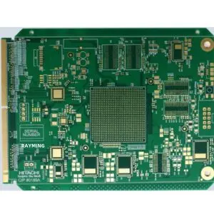
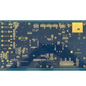
A micro via is a tiny hole drilled in a PCB that connects different layers of the board. Unlike standard vias, micro vias are significantly smaller, typically measuring less than 150 micrometers (μm) in diameter. These miniature connections play a vital role in creating more compact and efficient circuit designs, particularly in HDI boards.
Key Characteristics of Micro Vias
- Diameter: Usually less than 150 μm
- Aspect ratio: Typically 1:1 or less
- Depth: Often limited to connecting adjacent layers
- Manufacturing method: Laser drilling or photo-defined processes
Micro vias have revolutionized PCB design by allowing for higher component density and improved signal integrity, making them indispensable in modern electronics manufacturing.
Advantages of Using Micro Vias
The incorporation of micro vias in PCB design offers numerous benefits that have made them increasingly popular in the electronics industry. Let’s explore some of the key advantages:
1. Increased Circuit Density
Micro vias allow for more components to be placed on a board, significantly increasing circuit density. This is particularly crucial for compact devices like smartphones and wearables.
2. Improved Signal Integrity
By reducing the length of signal paths, micro vias help minimize signal distortion and improve overall signal integrity. This is especially important for high-frequency applications.
3. Enhanced Thermal Management
The smaller size of micro vias allows for better heat dissipation, contributing to improved thermal management in densely packed boards.
4. Reduced Layer Count
In some designs, micro vias can help reduce the total number of layers required in a PCB, potentially lowering manufacturing costs.
5. Flexibility in Design
Micro vias offer designers more flexibility in routing traces and placing components, enabling more efficient and optimized layouts.
Microvia vs Via: Understanding the Differences
While micro vias and standard vias serve similar purposes, there are significant differences between the two. Understanding these distinctions is crucial for PCB designers and manufacturers.
Standard Vias
- Diameter: Typically 300 μm or larger
- Depth: Can span multiple layers
- Manufacturing method: Mechanical drilling
- Applications: Suitable for most conventional PCB designs
Micro Vias
- Diameter: Less than 150 μm
- Depth: Usually limited to connecting adjacent layers
- Manufacturing method: Laser drilling or photo-defined processes
- Applications: Essential for HDI boards and compact designs
The choice between micro vias and standard vias depends on factors such as board density, signal integrity requirements, and manufacturing capabilities.
Read more about:
What are the Types of Microvias?
Micro vias come in several types, each with its own characteristics and applications. Understanding these variations is crucial for optimizing PCB design.
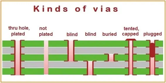
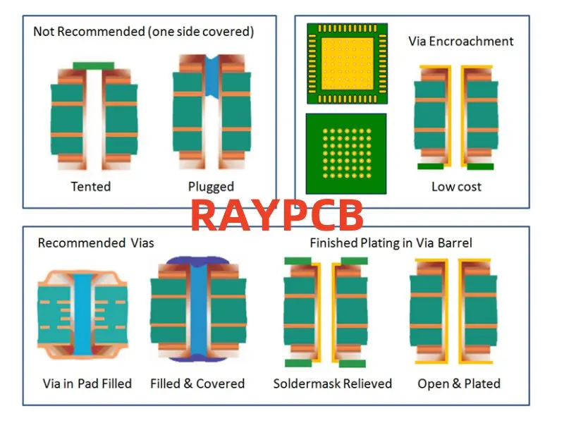
1. Blind Microvias
Blind microvias connect an outer layer to one or more inner layers but do not extend through the entire board.
Advantages:
- Increased routing density on outer layers
- Improved signal integrity for high-speed signals
Applications:
- High-frequency circuits
- Mobile devices
2. Buried Microvias
Buried microvias are internal connections that do not reach any outer layer of the PCB.
Advantages:
- Maximizes available space on outer layers
- Reduces electromagnetic interference (EMI)
Applications:
- Complex multilayer boards
- Designs requiring high signal isolation
3. Stacked Microvias
Stacked microvias are a series of micro vias placed directly on top of each other, connecting multiple layers.
Advantages:
- Enables connections across multiple layers
- Reduces the number of vias required
Applications:
- Very high-density designs
- Boards with limited surface area
4. Staggered Microvias
Staggered microvias are offset from each other rather than stacked directly on top of one another.
Advantages:
- Improved reliability compared to stacked microvias
- Better distribution of thermal stress
Applications:
- Designs requiring a balance between density and reliability
- Boards subject to thermal cycling
5. Via-In-Pad Microvias
Via-in-pad microvias are placed directly in the pad of a component.
Advantages:
- Reduces required board space
- Improves signal integrity by shortening signal paths
Applications:
- Ball Grid Array (BGA) components
- Ultra-compact designs
How to Manufacture Micro Via Holes
The manufacturing process for micro via holes is a critical aspect of HDI board production. The most common methods include:
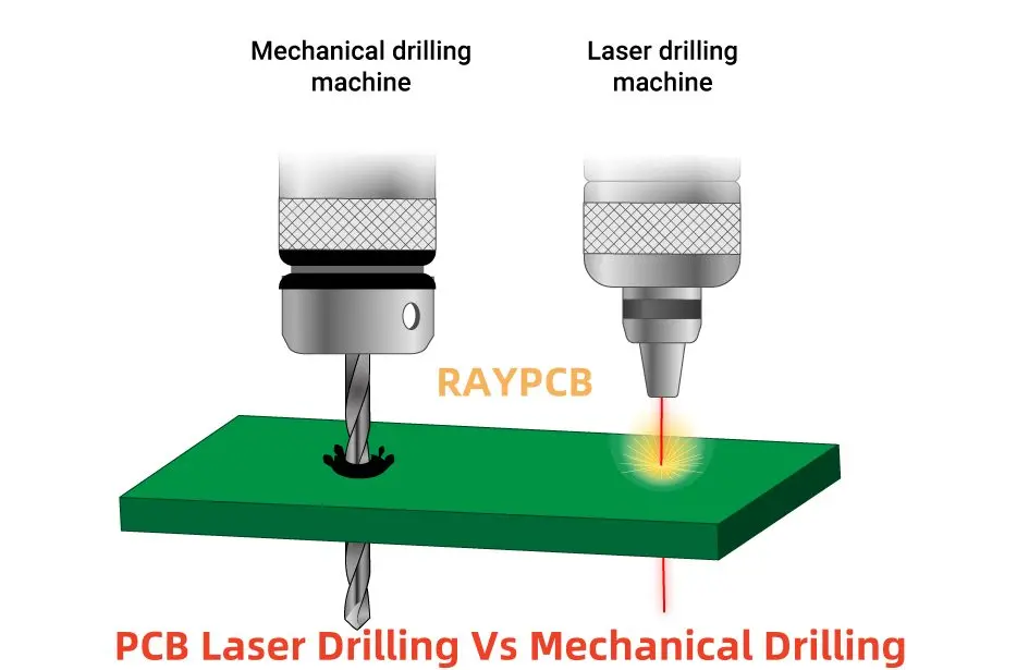
1. Laser Drilling
Laser drilling is the primary method for creating micro vias. It offers several advantages:
- Precision: Capable of creating very small, accurate holes
- Speed: Can drill thousands of holes per second
- Flexibility: Can be used on various materials
The process involves using a computer-controlled laser to ablate the material, creating the micro via hole.
2. Photo-Defined Vias
This method uses photosensitive materials and UV light to create micro vias:
- Apply photosensitive dielectric material
- Expose to UV light through a mask
- Develop the material to reveal the micro via holes
Photo-defined vias offer excellent precision but are generally slower than laser drilling.
3. Plasma Etching
While less common, plasma etching can be used to create micro vias in certain materials:
- Uses ionized gas to remove material
- Can create very small, high-aspect-ratio vias
- Typically used in specialized applications
Resin Filling and Copper Plating for Microvias
After creating micro via holes, two crucial steps follow: resin filling and copper plating.
Resin Filling
Resin filling involves:
- Applying epoxy resin to fill the micro via holes
- Curing the resin to create a solid, flat surface
- Planarizing the surface to ensure evenness
Benefits of resin filling:
- Improves structural integrity
- Enhances thermal management
- Provides a flat surface for subsequent layers
Copper Plating
Copper plating is essential for creating electrical connections:
- Apply a thin layer of copper using electroless plating
- Build up copper thickness using electrolytic plating
- Pattern and etch the copper to create the desired circuitry
Importance of copper plating:
- Creates reliable electrical connections
- Enhances current-carrying capacity
- Improves signal integrity
Design Guidelines for Micro Via in PCB
Designing PCBs with micro vias requires careful consideration of several factors:
1. Via Size and Aspect Ratio
- Keep aspect ratios (depth to width) at 1:1 or less for reliability
- Consider manufacturing capabilities when specifying via sizes
2. Via Placement
- Avoid placing micro vias in high-stress areas
- Consider signal integrity when determining via locations
3. Stack-Up Design
- Plan layer stack-up carefully to minimize the number of micro vias required
- Consider using hybrid designs with both micro vias and standard vias
4. Thermal Management
- Be aware of potential heat concentration in areas with many micro vias
- Consider thermal vias for improved heat dissipation
5. Signal Integrity
- Use simulation tools to verify signal integrity in designs with micro vias
- Consider impedance control for high-speed signals
6. Manufacturing Tolerances
- Work closely with your PCB manufacturer to understand their capabilities and tolerances
- Design with manufacturing yield in mind to reduce costs
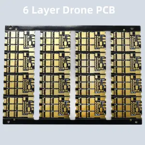
Applications of Microvia PCB
Micro via technology has found applications in various industries and products:
1. Consumer Electronics
- Smartphones
- Tablets
- Wearable devices
2. Automotive Industry
- Advanced driver-assistance systems (ADAS)
- Infotainment systems
- Electric vehicle control units
3. Aerospace and Defense
- Satellite communications
- Radar systems
- Avionics
4. Medical Devices
- Implantable devices
- Portable diagnostic equipment
- Imaging systems
5. Telecommunications
- 5G infrastructure
- High-speed networking equipment
- Optical transceivers
6. Industrial Applications
- IoT devices
- Robotics
- Process control systems
Conclusion
Micro via technology has become an essential component in the world of PCB design, particularly for HDI boards. By enabling higher circuit densities, improved signal integrity, and more flexible designs, micro vias have paved the way for the development of smaller, faster, and more complex electronic devices.
As technology continues to advance, the importance of micro vias in PCB design is only expected to grow. PCB designers and manufacturers must stay abreast of the latest developments in micro via technology to remain competitive in the rapidly evolving electronics industry.
By understanding the types, manufacturing processes, design guidelines, and applications of micro vias, electronics professionals can harness the full potential of this technology to create innovative and high-performance products that meet the demands of today’s market and beyond.