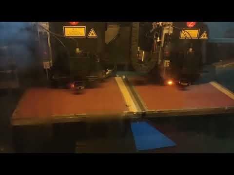
Laser drilling enables ultra-precise hole formation in PCBs, creating critical interlayer connections that power today’s advanced electronics. This technology is essential for manufacturing high-density interconnect (HDI) boards found in modern slim devices like smartphones and wearables. Unlike mechanical drilling, laser systems achieve unmatched accuracy—even at microscopic scales—ensuring reliability in increasingly miniaturized designs.
The process harnesses concentrated laser energy (from CO₂ or UV sources) to vaporize material with pinpoint precision. As an acronym for Light Amplification by Stimulated Emission of Radiation, a laser’s coherent beam eliminates physical contact, avoiding mechanical stress and enabling cleaner, smaller holes than traditional drill bits can produce.
What is Circuit Board Drilling?
Circuit board drilling is a fundamental process in PCB manufacturing that involves creating holes in the board substrate. These holes serve various purposes, including:
- Mounting components
- Creating electrical connections between layers
- Facilitating the flow of signals and power
Traditionally, mechanical drilling has been the go-to method for creating these holes. However, as PCB designs become more complex and miniaturized, laser drilling has gained prominence, especially for creating smaller, more precise holes.
Why is Laser Drilling Required for PCB?
Laser drilling has become increasingly essential in PCB manufacturing due to several factors:
1. Miniaturization
As electronic devices become smaller and more powerful, PCBs must accommodate more components in less space. Laser drilling allows for the creation of extremely small holes, enabling higher component density.
2. High-Density Interconnect (HDI) Boards
HDI boards require a large number of small, precise holes to connect multiple layers. Laser drilling is ideal for creating these microvias efficiently.
3. Precision
Laser drilling offers unparalleled accuracy in hole placement and size, which is crucial for advanced PCB designs.
4. Material Compatibility
Lasers can drill through a wide range of PCB materials, including those that are difficult to process with mechanical drills.
5. Non-Contact Process
Unlike mechanical drilling, laser drilling is a non-contact process, reducing the risk of damage to delicate board structures.
Read more about:
How Small of a Hole Can a Laser Drill?
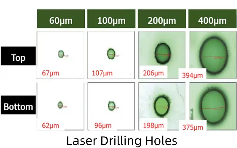
One of the most significant advantages of laser drilling is its ability to create extremely small holes. The size of holes that can be laser-drilled depends on several factors, including:
- The type of laser used
- The material being drilled
- The thickness of the PCB
Typically, laser drilling can create holes as small as 25 microns (0.001 inches) in diameter. Some advanced systems can even produce holes as small as 10 microns. This capability is crucial for creating microvias in HDI boards and enabling the production of increasingly compact electronic devices.
Advantages of Laser Drilling
Laser drilling offers numerous advantages over traditional mechanical drilling methods:
1. Precision and Accuracy
Lasers can create holes with extremely tight tolerances, ensuring consistent size and placement.
2. High-Speed Processing
Laser drilling can be performed at very high speeds, increasing productivity in PCB manufacturing.
3. Flexibility
Laser systems can be quickly reprogrammed to accommodate different hole patterns without changing physical tooling.
4. Reduced Wear and Tear
As a non-contact process, laser drilling eliminates the need for physical drill bits, reducing maintenance and replacement costs.
5. Clean Process
Laser drilling produces less debris and doesn’t require cutting fluids, resulting in a cleaner manufacturing environment.
6. Ability to Drill at Angles
Some laser systems can drill holes at angles, which is difficult or impossible with mechanical drilling.
7. Suitable for Delicate Materials
Laser drilling can process thin and fragile materials without causing damage or delamination.
Different Methods of Laser Drilling
Laser drilling techniques have evolved to meet various manufacturing needs. Here are the primary methods used in PCB production:
1. Single-pulse/Shot Laser Drilling
This method uses a single, high-energy laser pulse to create a hole.
Advantages:
- Very fast process
- Suitable for thin materials
Limitations:
- Limited hole depth
- May not be suitable for all materials
2. Percussion Laser Drilling
Percussion drilling uses multiple laser pulses to gradually create a hole.
Advantages:
- Can create deeper holes than single-pulse drilling
- Offers better control over hole shape
Limitations:
- Slower than single-pulse drilling
- May cause more heat-affected zones around the hole
3. Trepanning
Trepanning involves using the laser to cut around the circumference of the desired hole.
Advantages:
- Can create larger holes with very smooth walls
- Allows for precise control of hole diameter
Limitations:
- Slower than other methods for small holes
- May not be suitable for very small hole sizes
4. Helical Laser Drilling
This method uses a rotating laser beam to create holes in a spiral pattern.
Advantages:
- Can create deep holes with high aspect ratios
- Produces very smooth hole walls
Limitations:
- Requires specialized equipment
- May be slower for certain applications
Which Lasers are Suitable for Drilling Micro Holes?
Several types of lasers are used for drilling micro holes in PCBs, each with its own strengths:
1. Excimer Lasers
- Ideal for creating very small, precise holes
- Commonly used for microvias in HDI boards
2. Solid-State Lasers
- Include Nd:YAG and fiber lasers
- Offer good precision and are suitable for a range of materials
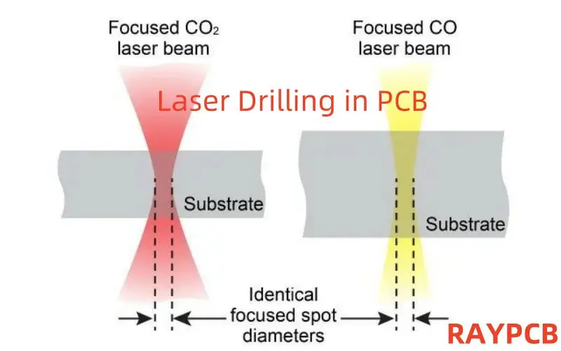
3. CO2 Lasers
- Widely used for drilling in organic PCB materials
- Cost-effective for many applications
4. Ultrafast Lasers
- Include femtosecond and picosecond lasers
- Provide extremely high precision with minimal heat-affected zones
The choice of laser depends on factors such as the PCB material, required hole size, and production volume.
Types of Laser Drilling Machines
Laser drilling machines come in various configurations, each suited to different PCB manufacturing needs:
1. CO2 Lasers
CO2 lasers are widely used in PCB manufacturing due to their versatility and cost-effectiveness.
Advantages:
- Excellent for drilling organic PCB materials
- High power output for fast processing
- Relatively low operating costs
Limitations:
- Limited in drilling very small holes (typically >75 microns)
- Not suitable for some metal-based materials
2. Nd:YAG Lasers
Nd:YAG (Neodymium-doped Yttrium Aluminum Garnet) lasers offer high precision for micro-drilling applications.
Advantages:
- Can drill very small holes (<50 microns)
- Suitable for a wide range of materials, including metals
- High peak power for efficient drilling
Limitations:
- Higher initial cost compared to CO2 lasers
- May require more maintenance
3. Combination of Nd:YAG and CO2 Laser Processes
Some advanced PCB manufacturing systems combine both Nd:YAG and CO2 lasers to leverage the strengths of each technology.
Advantages:
- Versatility to handle a wide range of materials and hole sizes
- Optimized processing for different PCB layers
Limitations:
- Higher system complexity and cost
- Requires expertise to manage multiple laser technologies
PCB Laser Drilling vs Mechanical Drilling
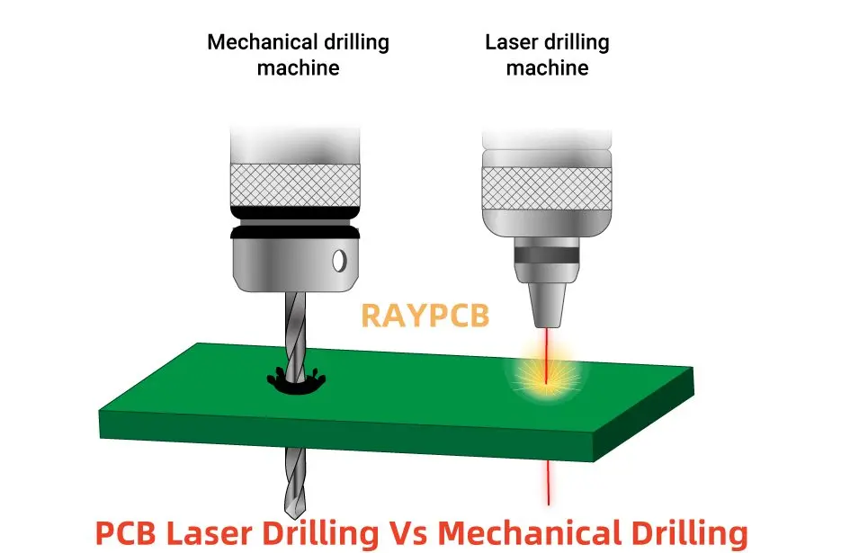
While both laser and mechanical drilling have their place in PCB manufacturing, it’s important to understand their differences:
Laser Drilling
Advantages:
- Can create extremely small holes (down to 10-25 microns)
- Non-contact process, reducing wear and tear
- High precision and repeatability
- Suitable for delicate and thin materials
Limitations:
- Higher initial equipment cost
- Limited in creating larger holes efficiently
- May have issues with certain materials (e.g., some metals)
Mechanical Drilling
Advantages:
- Cost-effective for larger hole sizes
- Can drill through multiple board layers efficiently
- Suitable for a wide range of hole sizes
Limitations:
- Limited in creating very small holes (<75 microns typically)
- Tool wear can affect precision over time
- May cause burrs or rough edges requiring post-processing
The choice between laser and mechanical drilling often depends on the specific requirements of the PCB design, production volume, and available budget.
Facts about PCB Laser Drilling Cost
While laser drilling offers many advantages, cost is an important consideration for manufacturers. Here are some key facts about PCB laser drilling costs:
1. Initial Investment
Laser drilling equipment requires a significant upfront investment, often higher than mechanical drilling systems.
2. Operating Costs
- Lower consumable costs (no drill bits to replace)
- Potentially higher energy consumption
- Specialized maintenance may be required
3. Throughput Considerations
- Laser drilling can be faster for small holes, potentially reducing per-unit costs
- For larger holes, mechanical drilling may be more cost-effective
4. Material Costs
Some materials optimized for laser drilling may be more expensive than standard PCB materials.
5. Long-Term Cost Benefits
- Reduced need for rework due to higher precision
- Ability to produce more complex boards, potentially increasing product value
6. Scalability
Laser drilling systems can often be scaled more easily to meet increased production demands.
While the initial cost of laser drilling may be higher, it can offer long-term cost benefits, especially for high-volume production of complex PCBs.
Laser-Drilled Microvia-in-Pad Technology in Your HDI PCB
Laser-drilled microvia-in-pad technology is a crucial advancement in High-Density Interconnect (HDI) PCB design. This technique involves creating small, laser-drilled vias directly in the pad of a component, offering several benefits:
1. Increased Routing Density
By placing vias directly in component pads, designers can achieve higher routing density and more efficient use of board space.
2. Improved Signal Integrity
Shorter connection paths reduce signal degradation and improve overall signal integrity.
3. Enhanced Thermal Performance
Microvia-in-pad can improve thermal dissipation, crucial for high-power components.
4. Reduced Board Size
This technology allows for more compact PCB designs, essential for miniaturized electronic devices.
5. Support for Advanced Packaging
Microvia-in-pad is crucial for supporting advanced component packages like Ball Grid Arrays (BGAs) with fine pitches.
Implementation Considerations:
- Requires precise control of laser drilling parameters
- May need specialized PCB materials for optimal performance
- Demands careful attention to plating and filling processes
As electronic devices continue to shrink while increasing in functionality, microvia-in-pad technology enabled by laser drilling will play an increasingly important role in PCB design and manufacturing.
Conclusion
Laser drilling has revolutionized PCB manufacturing, enabling the production of increasingly complex and miniaturized electronic devices. Its ability to create precise, small-diameter holes is crucial for high-density interconnect boards and advanced packaging technologies.
While laser drilling offers numerous advantages in terms of precision, flexibility, and ability to work with delicate materials, it’s important to consider factors such as cost, specific application requirements, and material compatibility when choosing between laser and mechanical drilling methods.
As technology continues to advance, we can expect further innovations in laser drilling techniques and equipment, potentially opening up new possibilities in PCB design and electronics manufacturing. Manufacturers and designers who stay abreast of these developments will be well-positioned to create cutting-edge electronic products that meet the ever-increasing demands of the modern world.
Whether you’re a PCB designer, a manufacturer, or simply someone interested in the intricacies of electronics production, understanding laser drilling technology is key to appreciating the complexity and precision that goes into every electronic device we use in our daily lives.