Layer mapping & region boundaries
Identify exactly which layers continue between rigid islands. Draw no-flow prepreg, coverlay, adhesive and local reinforcement extents.

RAYPCB / Manufacturing specifications
Review the complete rigid-flex construction, then check the rigid and flexible regions against their own geometry and process limits.
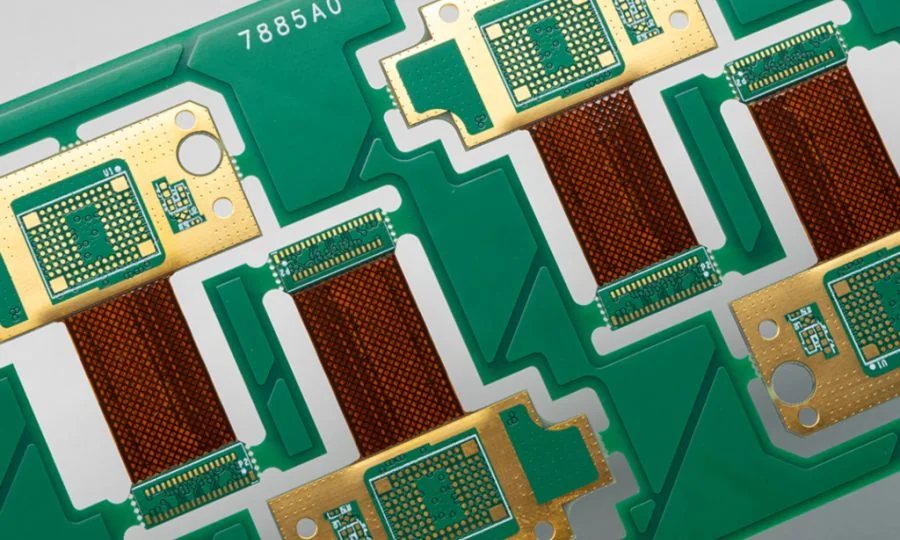
Use the matching construction and production window. Dimensions, copper and via limits must be reviewed together; an extended capability is confirmed against the released drawing.
Capability tables (CSV)| Parameter | Specification | Application notes |
|---|---|---|
| Rigid-flex total layers | 2–32 layers | |
| Flexible layers (within) | 1–12 layers | |
| Rigid base material | FR-4 (High-Tg 150 / 170 available) | |
| Flex base material | Polyimide (PI / Kapton), PET, PEN | |
| Coverlay | Polyimide coverlay on flex areas | |
| Stiffeners | FR4, aluminum, polyimide, stainless steel | |
| Finished thickness (rigid-flex) | 0.06–4.0 mm; define rigid and free-flex regions separately | |
| Copper weight | Flex 1/3 oz – 2 oz · rigid heavy copper to 12 oz | |
| Flex-section min trace / space | 0.5 oz: 4/4 mil · 1 oz: 5/5 mil · 2 oz: 5/7 mil | |
| Through-hole aspect ratio | Up to 10:1 reference | Apply to the through-hole depth/diameter definition, not a laser microvia. |
| Blind-via aspect ratio | Up to 0.75:1 reference | Confirm dielectric depth, opening definition and the selected manufacturing process. |
Flexible copper is part of the total layer count, not an addition to it. Flex copper limits apply only to the flexible region; high copper weights belong to rigid-region review.
| Parameter | Mass production | Prototype / extended review | Application notes |
|---|---|---|---|
| Min. inner-layer clearance | 3 mil | 3 mil | |
| Min. line width | 3 mil (0.0762 mm) | 3 mil (0.0762 mm) | |
| Min. line space | 3 mil (0.0762 mm) | 3 mil (0.0762 mm) | |
| Min. hole size | 0.1 mm | 0.1 mm | 0.1 mm drill/process entry; earlier finished-hole reference is 0.152 mm. They are not equivalent dimensions. |
| Min. plated hole copper | 25 µm | 25 µm | Plated-through-hole reference; specify average/local minimum and acceptance class. |
| Min. blind / buried via | 0.1 mm | 0.1 mm (1–18 layers) | Define layer span, depth and opening diameter; confirm the complete via map. |
| PTH dia. tolerance | ±0.076 mm (≈±3 mil) | ±0.076 mm (≈±3 mil) | |
| NPTH dia. tolerance | ±0.05 mm (≈±2 mil) | ±0.05 mm (≈±2 mil) | |
| Hole position deviation | ±0.05 mm (≈±2 mil) | ±0.05 mm (≈±2 mil) |
The 3 mil conductor values below refer to rigid regions. Use the copper-dependent flex values in the construction table for flexible tails. Confirm finished-hole diameter separately from drilling.
| Parameter | Mass production | Prototype / extended review | Application notes |
|---|---|---|---|
| Heavy copper (rigid) | 4 oz (nominal ≈140 µm) | up to 12 oz | Review copper with line/space and construction; do not combine independent minima. |
| Min. solder-mask bridge | 0.1 mm (≈4 mil) | 0.1 mm (≈4 mil) | |
| Solder-mask colour | Green, Black, Blue, White, Yellow, Red | Green, Black, Blue, White, Yellow, Red | |
| Silkscreen colour | White, Yellow, Red, Black | White, Yellow, Red, Black | |
| Peelable mask | Top, bottom, double-sided | Top, bottom, double-sided |
A 12 oz rigid-region option does not qualify a 12 oz flexible tail. Review copper balance, transition geometry and lamination for the complete board.
| Parameter | Mass production | Prototype / extended review |
|---|---|---|
| Outline method | Routing, V-groove, beveling, punch | Routing, V-groove, beveling, punch |
| Outline tolerance | ±0.15 mm (≈±6 mil) | ±0.15 mm (≈±6 mil) |
Specify each rigid outline, flex outline and transition boundary. V-scoring is a rigid-area option and must not cut a flexible interconnect.
| Parameter | Mass production | Prototype / extended review | Application notes |
|---|---|---|---|
| Controlled impedance | ±10% | ±7% | Agree signal/reference layers, geometry, coupon and test method. |
| Insulation resistance | 1 × 10¹² Ω (normal) | 1 × 10¹² Ω (normal) | Confirm temperature, humidity, conditioning and test voltage. |
| Through-hole resistance | Per approved continuity test plan | Per approved continuity test plan | Continuity threshold and unit must be specified in the electrical-test plan. |
| Thermal shock | 3 × 10 sec @ 288 ℃ | 3 × 10 sec @ 288 ℃ | Confirm specimen, conditioning, cycles and acceptance method; not an operating-temperature rating. |
| Warp & twist | ≤ 0.7% | ≤ 0.7% | Define the panel/board condition and measurement method. |
| Electric strength | > 1.3 kV/mm | > 1.4 kV/mm | Material test reference; confirm test method and dielectric construction. |
| Peel strength | 1.4 N/mm | 1.4 N/mm | Confirm laminate, copper, conditioning and test method. |
| Solder-mask hardness reference | > 6H | > 6H | Reference >6H; specify the hardness test method. Do not interpret this as an abrasion-life rating. |
| Flammability | 94V-0 material / construction option | 94V-0 material / construction option | For the selected recognized material/construction; request the applicable UL file and thickness range. |
| Test voltage | 50–330 V | 50–330 V | Electrical-test setting; not rated operating voltage. |
Impedance must be reviewed across transitions. Flatness, thermal stress and peel criteria require defined specimens and conditions; they do not replace bend-life qualification.
Select the rigid laminate, flexible film, adhesive, coverlay and no-flow prepreg as one compatible system. Finish options include ENIG, ENEPIG, OSP, immersion silver / tin, and electrolytic hard gold / gold fingers.
State the finish and required thickness or specification on the drawing. Material ratings and finish acceptance apply to the selected construction.
Identify exactly which layers continue between rigid islands. Draw no-flow prepreg, coverlay, adhesive and local reinforcement extents.
Unbonded flex layers can change bending behaviour. Define lengths, edge treatment and mechanical duty rather than assuming a universal bend improvement.
Show stacked or staggered via spans and the lamination order. Keep microvia depth ratios separate from through-hole aspect ratio.
Prepare the region stackup and export the result if useful. The workbench is a planning aid; the capability tables remain the reference for your drawing review.
Agree IPC-6013 for flexible / rigid-flexible board performance and IPC-A-600 for board acceptability, including revision, class and customer requirements. Request the relevant evidence against the part number and drawing revision.
IPC standards and their scope help separate manufacturing requirements from acceptance criteria.
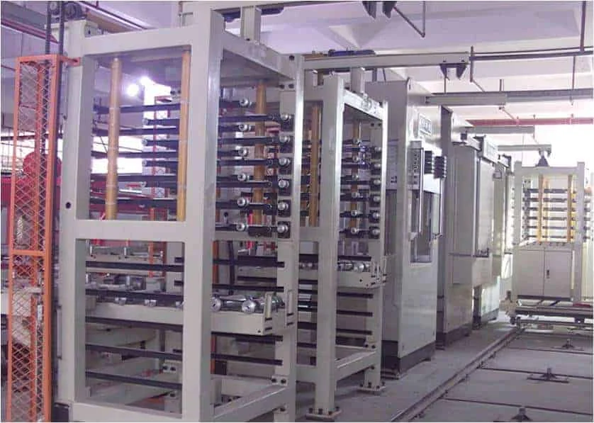
Quality system and supplier documents · Inspection workflow · Equipment and process evidence
No. If the two flexible copper layers continue within the six-layer rigid stack, the total is six. The region map must show which two layers continue.
Use the flex line/space entry for its copper weight. The rigid-region table is not an interchangeable flex design rule.
It is the construction range requiring region-specific definition. State the thickness of every rigid region and free-flex region separately; it is not a universal bending thickness.
Send what you have. Mark any requirement where you need an engineering recommendation, and identify the current revision.
Ready for a manufacturability review?
Upload the files through Contact. The reply can define pricing, delivery, process exceptions and the agreed test scope.
Send files for an exact quote