
RAYPCB · Heavy copper specifications
3 oz Copper PCB: choose copper by the loss you need to reduce
Compare 105 µm nominal copper with a wider 2 oz path. Review voltage drop, finished thickness and fabrication costs before choosing your power-board construction.
Share your current requirements and open questions. Tool use is optional.
What is a 3 oz copper PCB?
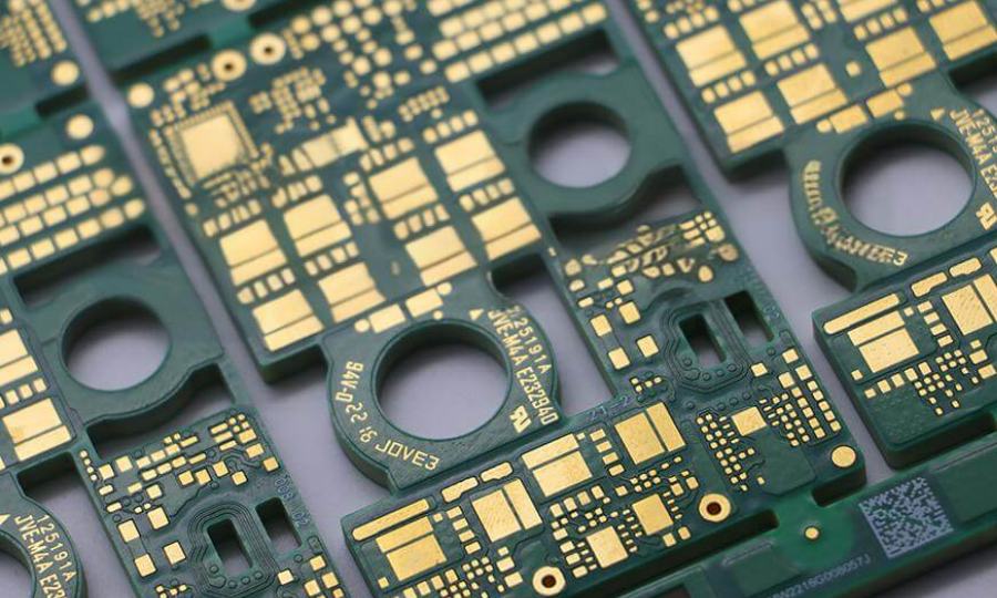
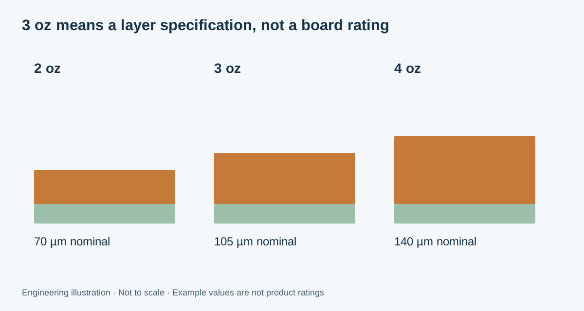
A 3 oz copper PCB specifies approximately 3 ounces of copper per square foot on the identified copper layer, conventionally rounded to 105 µm, 0.105 mm or 4.13 mil. The number describes copper, not the complete board thickness. A four-layer board can use different weights on different layers. Write the layer map instead of assuming that “3 oz PCB” means every conductor has the same thickness.
Three ounces is a useful candidate when a power route loses too much voltage or dissipates too much power at the available width. It does not establish an ampere rating. A connector, small pad exit or interlayer connection may dominate the circuit even after the main trace is thickened. Choose copper against a defined problem and carry that requirement through fabrication and validation.
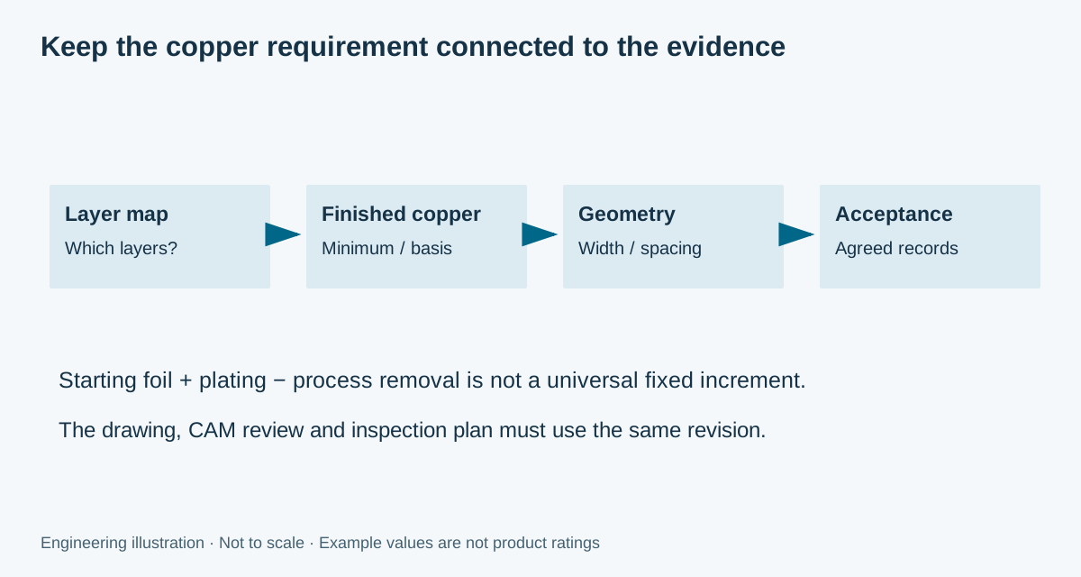
Nominal foil weight and minimum finished copper are different callouts. Outer-layer plating and process removal affect the finished conductor; there is no universal rule that 3 oz starting foil becomes exactly 4 oz finished copper. For inner layers, a nominal foil label also does not establish the minimum remaining copper after processing. IPC-4562 addresses metal foil; the finished-board drawing and agreed acceptance specification remain necessary.
Should you choose 2 oz, 3 oz or 4 oz?
Compare options at equal length and assumed copper temperature. Increasing thickness from 70 to 105 µm reduces ideal rectangular-trace resistance to two thirds. That is a resistance result, not a statement that permissible current increases by 50%. Temperature rise also depends on the board, nearby copper, cooling, load waveform and environment.
| Option | Nominal copper | Useful design question |
|---|---|---|
| 2 oz | 70 µm | Can a wider or shorter route meet the loss target? |
| 3 oz | 105 µm | Does extra cross-section solve the width constraint? |
| 4 oz | 140 µm | Is the additional reduction worth geometry and processing changes? |
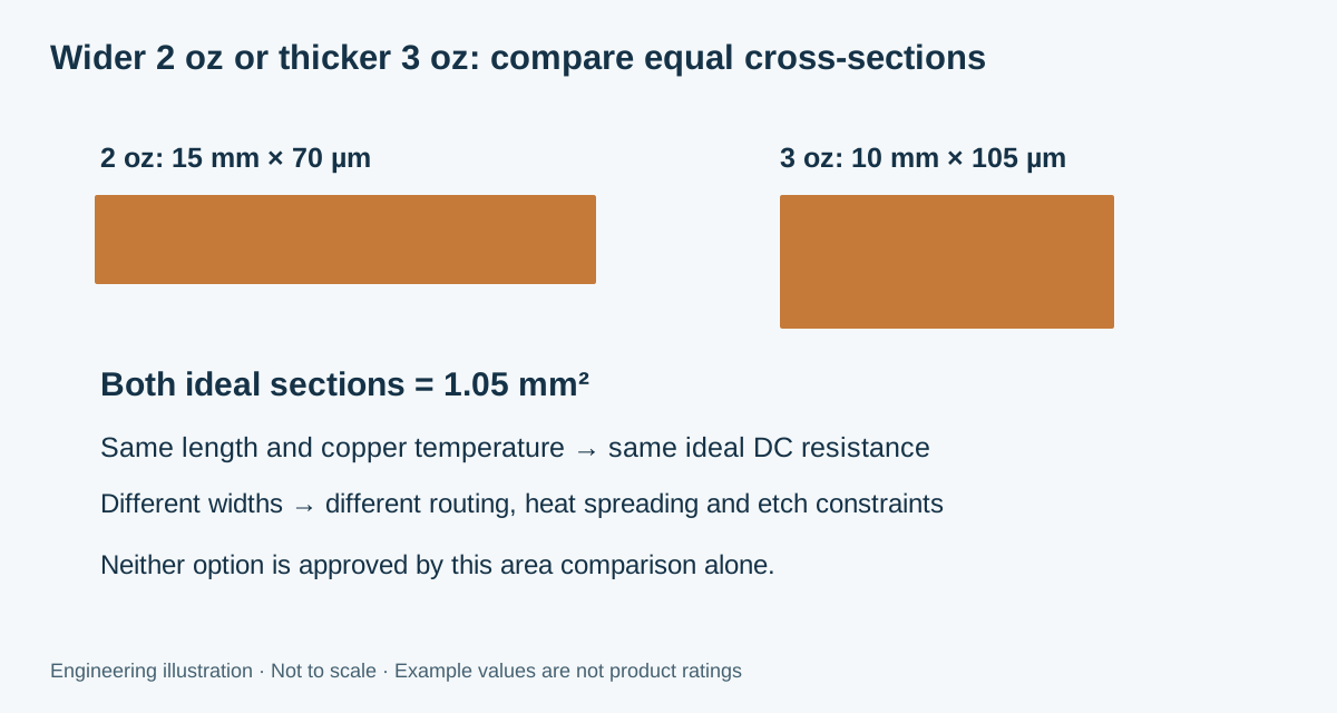
A 15 mm wide, 70 µm thick conductor has the same ideal cross-section as a 10 mm wide, 105 µm conductor: 1.05 mm². At equal length and temperature their DC resistances match. They occupy different routing areas and have different heat-spreading boundaries. A board with space for a wider path may therefore deserve a quotation alongside the thicker-copper option.
If the layout is already constrained at connector pads, review 4 oz finished conductor geometry before assuming the next copper weight will solve the problem. For broader construction choices, the heavy copper PCB guide compares the copper family and its manufacturing implications.
Compare DC loss and the width needed for a voltage-drop target
Enter the complete uniform path length, width, finished copper thickness, assumed conductor temperature and steady current. The comparison thickness changes only copper thickness; length and width stay the same. The additional width result answers one narrow question: what rectangular width would meet the entered voltage-drop target under these assumptions? It does not determine thermal safety or minimum manufacturable geometry.
RAYPCB ENGINEERING
Heavy Copper Specifications3 oz Copper Loss Comparison
Loading 3 oz Copper Loss Comparison…
The model uses R = ρL/A, V = IR and P = I²R. For 100 mm length, 10 mm width, 105 µm thickness and 20°C copper, resistance is about 1.642 mΩ. At 20 A, the calculated drop is 32.84 mV and loss is 0.657 W. Changing only thickness to 70 µm gives about 2.463 mΩ and 0.985 W. A 30 mV target at 20 A would require about 10.95 mm width in the selected 105 µm conductor.
These are reproducible electrical examples. They omit necks, vias, joints and frequency effects. TI's power-layout material explains conductor resistance as a layout concern. Use a thermal method appropriate to the complete assembly to turn an electrical-loss estimate into a temperature assessment.
Design the route, pads and return path together
Start with the actual current loop: source connector, switching or protection devices, load connector and return. A large copper pour can still have a narrow exit around a mounting hole or between component pads. Review the shortest effective cross-section along the route, including thermal-relief spokes. If a section is visibly narrower, calculate it separately and add the series resistance rather than using an average width for the whole board.
For motor-control and DC distribution boards, do not merge sensitive current-sense routing into the high-current return simply because the copper is thick. Keep the intended sense connection and reference path explicit. Switching-loop inductance, return geometry and coupling remain layout problems; thicker copper does not automatically improve EMI or high-frequency performance.
Ask for finished width and gap review before releasing dense areas. A minimum trace that is electrically adequate may be unsuitable for the chosen etching process. Conversely, a large enough etch gap may still fail an application's electrical clearance or creepage requirements. Keep manufacturing geometry and insulation design as separate checks with separate evidence.
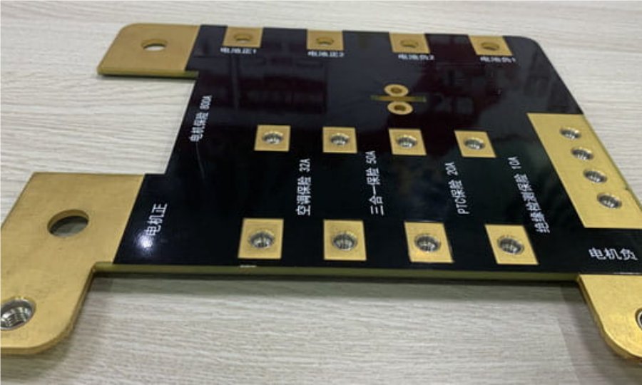
What the fabricator needs to resolve
Show which layers carry 3 oz, which retain lighter copper, the laminate grade and the finished thickness target. If the design includes fine-pitch components, state their critical pad and mask features. Keep a consistent revision across the artwork, drill data, fabrication drawing and stackup. The PCB DFM review is the next step when those requirements interact.
Etching changes the conductor profile. Plating, if used, changes surface and hole construction according to the process. Solder mask must cover the actual topography while leaving the required pad openings. Do not solve these details by adding a guessed artwork enlargement: the factory may already apply compensation, creating a second unintended change.
For a multilayer board, copper distribution and resin requirements matter as well as nominal weight. A symmetric list of copper weights does not prove that the layout is balanced. A large solid plane on one side and sparse traces on the other can behave differently during manufacture. Supply the complete pattern for stackup review rather than a copper-weight sentence alone.
What changes the cost of a 3 oz PCB?
Copper material is one driver; usable panel area, layer count, conductor geometry, material availability, tooling and inspection are others. The same 3 oz requirement can be straightforward on one layout and demanding on another. A fixed percentage premium over 1 oz or 2 oz cannot represent both boards. Request alternatives using the same revision, quantity, dimensions, finish and test scope.
The budget brief below records the copper-specific construction and adds allowances you already have. It can also generate a technical brief with all three cost fields blank. The explicit example is arithmetic practice, not a current RAYPCB price. Changing dimensions, quantity, layer map, currency or the allowance basis clears entered costs so an old quote is not silently reused for a changed design.
RAYPCB ENGINEERING
Heavy Copper Specifications3 oz Fabrication and Budget Brief
Loading 3 oz Fabrication and Budget Brief…
Compare the quoted unit amount and one-time charges together. A wider 2 oz alternative might alter board outline or panel utilization, while 3 oz might preserve the outline but require different processing. The relevant comparison is the quoted finished design. Use PCB quotation comparison when suppliers include different testing, shipping or engineering charges.
Prepare useful acceptance evidence
The copper callout should identify the layers, minimum finished requirement, measurement basis and exceptions. Agree which dimensions and cross-sections need evidence, and how results will be associated with the drawing revision. A catalog photograph shows a product example, not the measured minimum thickness of a new order.
Separate bare-board inspection from the product load test. Connectivity testing can check opens and shorts against the netlist; it does not show that a populated board meets its continuous-current requirement in an enclosure. A development test should use the intended current, ambient, cooling and connection arrangement, then examine the locations predicted to matter. Record the conditions so a later copper or layout change can be evaluated consistently.
For an enquiry, send the available manufacturing files, quantity breaks and target delivery milestone, plus the copper map and critical current path. Preliminary drawings are useful if open items are clearly named. You can request help before the loss model is complete; there is no need to invent a minimum thickness or a budget just to contact engineering.
3 oz PCB questions
How many amps can a 3 oz PCB carry?
There is no board-wide current value from copper weight alone. Length, width, temperature boundary conditions and every series connection matter. IPC-2152 addresses conductor size, current and temperature rise; the local tool only compares electrical loss.
Is 3 oz copper always 105 µm after fabrication?
105 µm is a rounded nominal reference. The accepted finished requirement depends on the drawing, process and agreed specification. State minimum finished copper separately from starting foil.
Does 3 oz copper make fine routing easier?
Do not assume so. Thick features change etching and topography. Review the actual finished width, spacing and mask features before committing to the layout.
Can I use 3 oz only on the power layers?
A mixed-copper construction may be worth reviewing. Specify all layers and the full stackup, including the signal layers and dielectric requirements. Manufacturing confirmation is specific to the combination.
Does the budget tool send my design automatically?
No. It runs locally and can download a text brief or open a mail draft. Attach the brief and files manually through Contact. An exact quotation follows review of the supplied requirements.
Request a 3 oz PCB review
Send the layer-by-layer copper requirement, fabrication revision, geometry, quantities and required evidence. Identify open construction or load questions so engineering can review a useful manufacturing proposal.
Attach a downloaded tool brief manually. Contact does not automatically receive these inputs. References reviewed September 2026. Illustrations use planning examples; photographs do not establish prices, delivery times or project-specific acceptance.