Introduction
In the ever-evolving world of electronics, Printed Circuit Boards (PCBs) serve as the backbone of nearly every device we use. At the heart of PCB design lies a crucial concept known as PCB stackup. Whether you’re a seasoned engineer or a budding electronics enthusiast, understanding PCB stackup is essential for creating efficient, reliable, and high-performing circuit boards.
What is a PCB Stackup?
A PCB stackup refers to the arrangement of copper layers, prepreg, and core materials that make up a printed circuit board. It defines the number of layers, their order, thickness, and the materials used between them. This configuration plays a pivotal role in determining the board’s electrical, mechanical, and thermal properties.
Importance of Proper PCB Stackup in Design and Manufacturing
The importance of a well-designed PCB stackup cannot be overstated. It directly impacts:
- Signal Integrity: Proper stackup minimizes crosstalk and EMI, ensuring clean signal transmission.
- Power Distribution: Effective power and ground plane placement for optimal power delivery.
- Thermal Management: Influences heat dissipation throughout the board.
- Manufacturing Yield: A well-planned stackup improves manufacturability and reduces defects.
- Cost Efficiency: Optimized stackups can reduce material usage and production costs.
Brief Overview: 4/6/8 Layers, Flex, Rigid-Flex
This comprehensive guide will delve into various PCB stackup configurations, including:
- Standard multilayer PCBs: 4-layer, 6-layer, and 8-layer designs
- Flexible PCB: Single and multi-layer flex circuits
- Rigid Flex PCB: Hybrid designs combining rigid and flexible sections
We’ll explore the unique characteristics, advantages, and applications of each type, providing you with the knowledge to choose the right stackup for your project.
1. Understanding PCB Stackup Basics

Definition of PCB Stackup
A PCB stackup is the cross-sectional view of a printed circuit board that details the number, order, and composition of layers. It’s essentially the blueprint of how the PCB is constructed, layer by layer.
Role of Layer Stackup in PCB Performance
The layer stackup directly influences several key aspects of PCB performance:
- Electrical Performance: Affects impedance control, signal integrity, and EMI shielding.
- Mechanical Stability: Determines the board’s physical strength and resistance to warping.
- Thermal Management: Influences heat distribution and dissipation.
- Reliability: Proper stackup design can enhance the long-term reliability of the PCB.
Key Elements: Layers, Materials, Dielectric, Copper Weight, Prepreg, Core
To fully grasp PCB stackup, it’s crucial to understand its key components:
- Layers: Copper layers where circuits are etched.
- Materials: Substrates like FR-4, Rogers, or polyimide.
- Dielectric: Insulating material between conductive layers.
- Copper Weight: Thickness of copper foil, measured in ounces per square foot.
- Prepreg: Pre-impregnated bonding material used to join layers.
- Core: A more rigid, cured material that provides structural support.
Common Applications for Multilayer PCBs
Multilayer PCBs find applications across various industries due to their versatility and performance benefits:
- Consumer Electronics: Smartphones, laptops, smart home devices
- Automotive: Engine control units, infotainment systems, safety features
- Aerospace: Avionics, satellite communications
- Medical Devices: Diagnostic equipment, implantable devices
- Industrial Controls: Factory automation, robotics
- Telecommunications: Network routers, 5G infrastructure
Read more about:
2. Standard PCB Stackups: 4, 6, and 8 Layers
2.1 4-Layer PCB Stackup
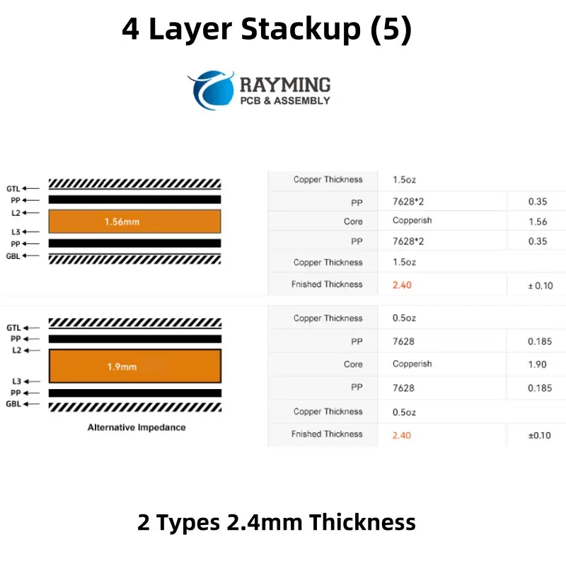
Typical Layer Arrangement
A standard 4-layer PCB stackup usually consists of:
- Top Signal Layer
- Ground Plane
- Power Plane
- Bottom Signal Layer
This arrangement provides a balance between cost and performance for many applications.
Signal Integrity, EMI Shielding, Power/Ground Planes
- Signal Integrity: The ground and power planes sandwiched between signal layers help reduce crosstalk and improve signal quality.
- EMI Shielding: The internal planes act as shields, reducing electromagnetic interference.
- Power/Ground Planes: Dedicated layers for power distribution ensure stable voltage supply and low impedance return paths.
Ideal Use Cases and Industries
4 layer PCBs are widely used in:
- Consumer electronics (e.g., digital cameras, smart home devices)
- Automotive electronics (e.g., sensor modules, control units)
- Industrial controls (e.g., PLC modules, HMI interfaces)
- IoT devices (e.g., smart sensors, wearables)
2.2 6-Layer PCB Stackup

Layer Structure Examples
A common 6 layer PCB stackup might include:
- Top Signal Layer
- Ground Plane
- Signal Layer
- Power Plane
- Signal Layer
- Bottom Ground Plane
This configuration offers more flexibility in routing and improved signal integrity compared to 4-layer designs.
Benefits over 4-Layer (Better EMI, Routing Density)
- Enhanced EMI Shielding: Additional ground layers provide better electromagnetic shielding.
- Increased Routing Density: More signal layers allow for complex routing in a compact space.
- Improved Signal Integrity: Better separation of high-speed signals from power/ground planes.
- Enhanced Power Distribution: Dedicated power and ground planes for cleaner power delivery.
Applications Needing High-Speed, Low Noise
6-layer PCBs are ideal for:
- High-speed digital circuits (e.g., high-performance computing)
- Analog/mixed-signal designs (e.g., data acquisition systems)
- RF and microwave applications (e.g., wireless communication modules)
- Medical imaging equipment
2.3 8-Layer PCB Stackup
Standard Stackup Configurations
An 8 layer PCB stackup might be arranged as follows:
- Top Signal Layer
- Ground Plane
- Signal Layer
- Power Plane
- Ground Plane
- Signal Layer
- Ground Plane
- Bottom Signal Layer
This configuration offers maximum flexibility and performance for complex designs.
High-Speed Design Requirements
8-layer PCBs are often necessary for high-speed designs due to:
- Improved Signal Isolation: Multiple ground planes minimize crosstalk.
- Enhanced Power Distribution: Dedicated power planes for different voltage requirements.
- Better Impedance Control: More options for controlling trace impedance.
- Reduced EMI: Multiple shielding layers for superior EMI performance.
Challenges and Solutions in 8-Layer Design
Challenges:
- Increased complexity in design and manufacturing
- Higher material costs
- Potential for increased thermal issues due to more layers
Solutions:
- Advanced PCB design software for complex stackup planning
- Careful thermal management techniques (e.g., thermal vias, copper pours)
- Collaboration with manufacturers to optimize for cost and performance
3. Advanced Stackup Types: Flex and Rigid-Flex PCBs
3.1 Flexible PCB Stackup
Flex PCB Layer Structures
Flexible PCBs can range from single-layer to multi-layer designs:
- Single-Layer Flex: One conductive layer on a flexible substrate
- Double-Layer Flex: Two conductive layers with a flexible core
- Multi-Layer Flex: Multiple conductive layers separated by flexible dielectric materials
Materials (Polyimide, Adhesiveless, etc.)
Common materials used in flex PCB stackups include:
- Polyimide: Offers excellent flexibility and heat resistance
- Adhesiveless Materials: Provide better flex life and dimensional stability
- Liquid Crystal Polymer (LCP): Suitable for high-frequency applications
- PTFE-based Materials: Used for high-speed, low-loss designs
Unique Challenges: Bending Radius, Layer Integrity
Flex PCBs face unique challenges:
- Bending Radius: Ensuring the PCB can bend without damaging traces or components
- Layer Integrity: Maintaining connections between layers during flexing
- Material Selection: Choosing materials that can withstand repeated bending
- Component Placement: Strategically placing components to minimize stress on solder joints
Typical Applications (Wearables, Aerospace)
Flex PCBs are commonly used in:
- Wearable Technology: Fitness trackers, smart clothing
- Aerospace: Satellite systems, aircraft control panels
- Medical Devices: Implantable electronics, hearing aids
- Automotive: Dashboard displays, steering wheel controls
- Consumer Electronics: Smartphone internal connections, camera modules
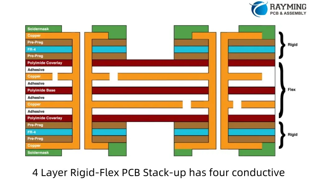
3.2 Rigid-Flex PCB Stackup
Hybrid Structures: Rigid + Flex
Rigid-flex PCBs combine rigid and flexible sections in a single board:
- Rigid Sections: Multi-layer stackups similar to standard PCBs
- Flex Sections: Single or multi-layer flexible circuits
- Transition Zones: Areas where rigid and flex sections connect
Stackup Planning for Dynamic Flexing
Considerations for rigid-flex stackup design include:
- Neutral Bend Axis: Positioning signal layers near the center of the flex section
- Adhesiveless Construction: Using adhesiveless materials in flex areas for better performance
- Copper Thickness: Balancing copper weight for flexibility and durability
- Layer Symmetry: Ensuring balanced construction to prevent warping
Cost vs. Benefit Considerations
Rigid-flex PCBs offer several benefits but at a higher cost:
Benefits:
- Space savings by eliminating connectors
- Increased reliability due to fewer interconnections
- Design flexibility for complex 3D applications
Costs:
- Higher material and manufacturing costs
- More complex design process
- Specialized manufacturing capabilities required
Common Use Cases
Rigid-flex PCBs are ideal for:
- Military and Aerospace: Compact, reliable electronics for harsh environments
- Medical Devices: Space-constrained applications like pacemakers or endoscopes
- Consumer Electronics: Foldable smartphones, laptop hinges
- Automotive: Instrument clusters, infotainment systems
- Industrial Equipment: Robotic arms, rotating or moving assemblies
4. Key Considerations When Designing PCB Stackups

Impedance Control and Signal Integrity
Proper impedance control is crucial for maintaining signal integrity:
- Trace Width and Spacing: Calculate based on desired impedance and layer thickness
- Reference Planes: Ensure consistent reference planes for high-speed signals
- Layer Ordering: Place high-speed signals adjacent to uninterrupted reference planes
- Differential Pair Routing: Maintain consistent spacing and length matching
Power Delivery and Grounding Strategies
Effective power distribution is essential for PCB performance:
- Plane Layer Allocation: Dedicate layers for power and ground planes
- Split Planes: Use split planes for multiple voltage requirements
- Decoupling Capacitors: Proper placement and selection of decoupling capacitors
- Return Path Planning: Ensure low-impedance return paths for all signals
Thermal Management
Consider thermal aspects in stackup design:
- Copper Weight: Heavier copper for improved heat dissipation
- Thermal Vias: Strategically placed vias to conduct heat between layers
- Material Selection: Choose materials with appropriate thermal conductivity
- Component Placement: Distribute heat-generating components across the board
Cost Implications of Layer Count and Material Choices
Balance performance requirements with cost considerations:
- Layer Count: More layers increase cost but improve performance
- Material Selection: High-performance materials (e.g., Rogers) increase cost
- Manufacturing Complexity: Tight tolerances and advanced techniques add to cost
- Volume Production: Consider scalability for large production runs
Manufacturability and Reliability Concerns
Ensure your stackup design is manufacturable and reliable:
- Aspect Ratio: Maintain proper hole aspect ratios for reliable plating
- Layer Symmetry: Balance copper distribution to prevent board warping
- Material Compatibility: Ensure all materials are compatible for lamination
- Design Rules: Adhere to manufacturer’s design rules for via sizes, trace widths, etc.
5. PCB Stackup for High-Speed and High-Frequency Designs
Importance of Controlled Impedance
Controlled impedance is critical in high-speed designs:
- Signal Reflection: Minimize reflections by matching trace impedance to source and load
- Signal Integrity: Maintain signal quality over long traces
- Timing: Ensure consistent signal propagation delays
How Stackup Affects Crosstalk, EMI, Signal Loss
Proper stackup design mitigates several issues:
- Crosstalk: Use ground planes between signal layers to reduce coupling
- EMI: Implement stripline configurations for better shielding
- Signal Loss: Choose low-loss materials and minimize layer transitions
Material Selection (FR4, Rogers, etc.) for RF/Microwave PCBs
Different materials offer varying performance at high frequencies:
- FR-4: Suitable for lower frequencies, cost-effective
- Rogers RO4350B: Low-loss material for high-frequency applications
- PTFE-based Materials: Excellent for mmWave and high-frequency designs
- Hybrid Stackups: Combine FR-4 and high-performance materials for cost-effective solutions
Best Practices for High-Speed Stackups
- Use ground-signal-ground (GSG) configurations for critical high-speed signals
- Implement continuous ground planes for uninterrupted return paths
- Minimize layer transitions for high-speed signals
- Use appropriate dielectric materials based on frequency requirements
- Employ advanced PCB design tools for accurate impedance and loss calculations
6. Comparing PCB Manufacturers’ Stackup Capabilities
ProtoExpress, Altium, PCBCart, PCBWay, JLCPCB Comparison
| Manufacturer | Layer Capability | Min. Line Width/Spacing | Special Materials | Flex/Rigid-Flex |
|---|---|---|---|---|
| ProtoExpress | Up to 40 layers | 3/3 mil | Yes | Yes |
| Altium | N/A (Design tool) | N/A | N/A | N/A |
| PCBCart | Up to 40 layers | 3/3 mil | Yes | Yes |
| PCBWay | Up to 16 layers | 3/3 mil | Yes | Yes |
| JLCPCB | Up to 16 layers | 3.5/3.5 mil | Limited | Yes |
Differences in Standard Stackup Offerings
- ProtoExpress and PCBCart offer the highest layer count capabilities
- PCBWay and JLCPCB are more focused on prototyping and small-scale production
- Altium provides design tools rather than manufacturing services
Material and Layer Capabilities
- High-end manufacturers offer a wide range of materials including Rogers, Taconic, and PTFE
- Budget-friendly options like JLCPCB may have more limited material choices
- Layer count capabilities vary, with some offering up to 40 layers for complex designs
Quality Certifications and Lead Times
- Most manufacturers hold ISO 9001 certifications
- Higher-end manufacturers often have additional certifications (e.g., AS9100 for aerospace)
- Lead times vary based on complexity and service level, ranging from 24 hours to several weeks
Price vs. Quality Analysis
- Higher layer counts and specialized materials increase costs
- Manufacturers like JLCPCB offer competitive pricing for standard designs
- ProtoExpress and PCBCart may have higher prices but offer more advanced capabilities
- Consider the balance between cost, quality, and required capabilities for your project
7. How to Choose the Right PCB Stackup for Your Project
Questions to Ask Before Designing
- What is the maximum frequency of operation?
- What are the impedance control requirements?
- How many layers are needed for routing and power distribution?
- Are there any specific EMI/EMC requirements?
- What are the mechanical and environmental constraints
- What is the expected production volume?
- Are there any specific regulatory requirements (e.g., UL, RoHS)?
- What is the budget for PCB fabrication?
- Are there any special requirements like flex or rigid-flex sections?
Working with Your PCB Manufacturer for Custom Stackups
- Engage Early: Consult with manufacturers during the design phase for optimal results.
- Provide Detailed Requirements: Clearly communicate your electrical and mechanical needs.
- Request DFM Analysis: Ask for Design for Manufacturability feedback on your stackup.
- Consider Their Expertise: Be open to suggestions from experienced fabricators.
- Discuss Material Options: Explore various material choices that meet your performance and budget requirements.
- Review Standard Offerings: Check if the manufacturer’s standard stackups can meet your needs before opting for fully custom designs.
Tools and Software for Stackup Planning (Altium, Cadence, etc.)
Several software tools can aid in PCB stackup design:
- Altium Designer: Offers a comprehensive stackup manager with impedance calculation.
- Cadence Allegro: Provides advanced stackup planning and analysis tools.
- Mentor Graphics HyperLynx: Specializes in signal integrity analysis for stackup optimization.
- Polar Instruments SI9000: Focused on impedance and insertion loss calculations.
- EDA Board Stackup: A web-based tool for quick stackup calculations and visualizations.
Key features to look for in stackup planning tools:
- Impedance calculation
- Loss modeling
- 3D visualization
- Integration with major EDA software
- Material library and customization options
8. Future Trends in PCB Stackup and Materials
Evolution Toward Thinner, Denser PCBs
As electronics continue to shrink, PCB stackups are evolving:
- Ultra-Thin Dielectrics: Manufacturers are developing reliable, ultra-thin dielectric materials.
- Microvias and Buried Vias: Increasing use of advanced via structures for higher density.
- Embedded Components: Integrating passive and active components within the PCB layers.
- High-Density Interconnect (HDI): More layers in thinner overall board thicknesses.
Materials Innovation (Low-Loss Dielectrics, Halogen-Free)
New materials are being developed to meet evolving needs:
- Low-Loss Materials: For high-frequency and high-speed applications.
- Halogen-Free Options: Meeting environmental and safety regulations.
- Thermally Conductive Dielectrics: Improving heat dissipation in dense designs.
- Bendable and Stretchable Substrates: For wearable and flexible electronics.
- Biodegradable PCB Materials: Addressing end-of-life environmental concerns.
Advanced Stackups for AI, 5G, Automotive, IoT
Emerging technologies are driving new stackup requirements:
- 1. AI and Machine Learning: High-layer count boards with optimized power delivery for AI accelerators.
- 2. 5G and mmWave: Ultra-low-loss materials and precise impedance control for high-frequency designs.
- 3. Automotive: Hybrid stackups combining high-temperature materials with standard FR-4 for cost-effectiveness.
- 4. IoT Devices: Flexible and rigid-flex designs for compact, energy-efficient devices.
- 5. Edge Computing: Stackups optimized for high-speed processing and thermal management in compact form factors.
Conclusio
Key Takeaways on PCB Stackup Importance
- PCB stackup is fundamental to board performance, affecting signal integrity, power distribution, and EMI.
- Proper stackup design can significantly improve manufacturability and reduce costs.
- Different applications require tailored stackup approaches, from simple 4-layer designs to complex rigid-flex configurations.
- Material selection is crucial, especially for high-speed and high-frequency applications.
- Advanced design tools and close collaboration with manufacturers are essential for optimal stackup design.
Encouragement to Plan Early with Manufacturers
Early engagement with PCB manufacturers can:
- Prevent costly design revisions
- Optimize stackups for performance and cost
- Ensure manufacturability of complex designs
- Leverage manufacturer expertise for innovative solutions
Don’t hesitate to consult with multiple manufacturers to find the best fit for your project’s unique requirements.
Resources for Further Reading and Professional Support
- IPC Standards: IPC-2141 (Controlled Impedance), IPC-6012 (Rigid PCB Qualification)
- Industry Journals: IEEE Transactions on Components, Packaging and Manufacturing Technology
- Online Communities: PCB Design007, EEVblog Forums
- Manufacturer Resources: Technical articles and webinars from major PCB fabricators
- Professional Organizations: IPC (Association Connecting Electronics Industries), SMTA (Surface Mount Technology Association)
FAQ Section
A: Core is a cured, rigid material that provides structural support, while prepreg is uncured, flexible material used to bond layers together during PCB fabrication.
A: Core is a cured, rigid material that provides structural support, while prepreg is uncured, flexible material used to bond layers together during PCB fabrication.
A: Proper stackup design, especially with strategic ground and power plane placement, can significantly reduce electromagnetic emissions and improve shielding effectiveness.
A: Yes, hybrid stackups are possible and often used to balance performance and cost, especially in high-frequency designs.
A: More layers and specialized materials increase cost. However, a well-designed stackup can reduce the need for additional components or complex routing, potentially lowering overall system cost.
A: While theoretically unlimited, practical limitations usually cap at around 40 layers. Most designs use 2 to 16 layers, with very complex boards using 20+ layers.
A: Use impedance calculation tools, consider trace width and spacing, maintain consistent reference planes, and work closely with your PCB manufacturer for precise control.
A: Yes, use high-Tg (glass transition temperature) materials, consider thermal expansion coefficients, and design for proper heat dissipation in your stackup.
By understanding and optimizing PCB stackup design, engineers can create more efficient, reliable, and cost-effective electronic products. As technology continues to advance, staying informed about the latest stackup techniques and materials will be crucial for success in PCB design and manufacturing.