
RAYPCB · Heavy copper specifications
10 oz Copper PCB: check the connections between thick conductors
A 350 µm nominal copper plane is one part of the circuit. Compare trace, plated-hole and connection resistance before choosing a 10 oz PCB construction.
Share your current requirements and open questions. Tool use is optional.
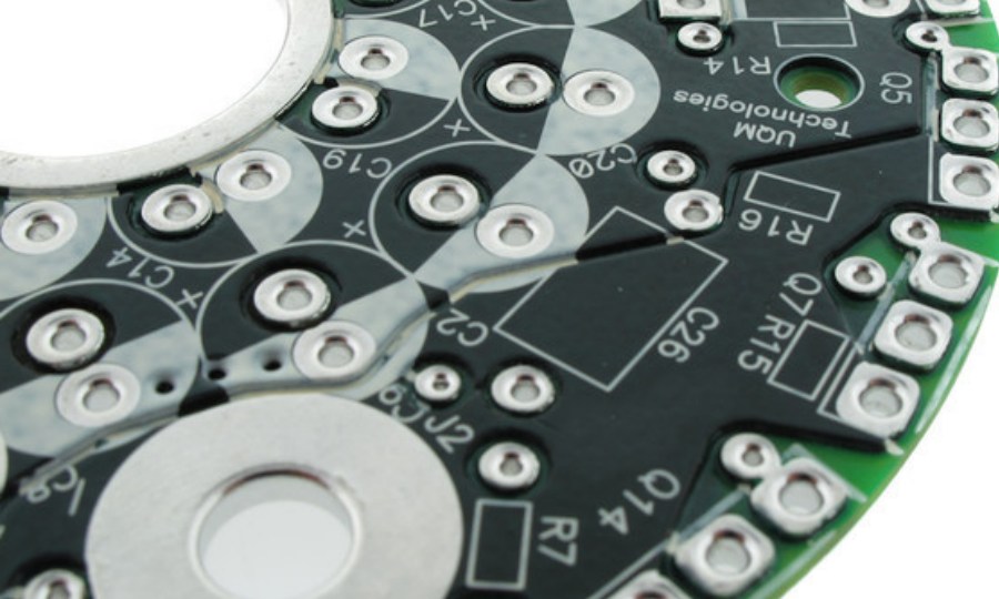
10 oz copper is a layer requirement, not a complete current path
A 10 oz copper PCB specifies approximately 350 µm, 0.350 mm or 13.78 mil nominal copper on identified conductive layers. The common conversion uses about 35 µm per oz/ft². It does not define finished board thickness or the copper deposited in a plated hole. State the layer map and minimum finished requirements explicitly instead of assuming that all copper features become equally thick.
Ten-ounce copper can be considered when the main power route needs substantial cross-section within the available width. Yet a low-resistance plane may connect through much smaller barrel walls, pad transitions or terminal interfaces. This page examines those series elements so the design review does not stop at the broadest part of the board.
The heavy copper PCB guide covers family-level material and process choices. For narrow in-plane sections, the 8 oz current-path comparison gives a separate neck-down example. Here the emphasis is the connection from one conductor to the next.
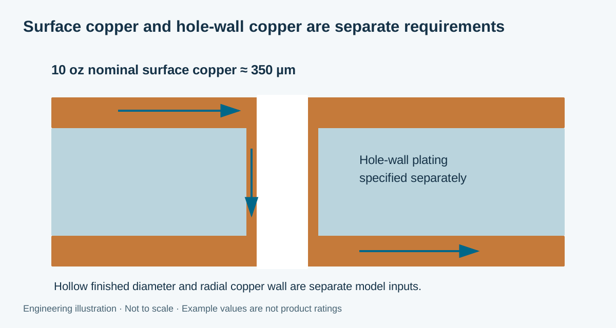
Keep surface copper and hole-wall copper separate
The nominal 350 µm surface conductor and a plated-through-hole wall are different dimensions. A hole's current path depends on its conducting length, finished inner diameter, copper wall thickness and connections to the pads or planes. A heavy outer layer does not by itself establish any of those values. Specify and inspect the interconnect construction independently.
For a hollow cylindrical barrel, conductor area is π[(D/2 + p)² − (D/2)²], where D is the finished hollow inner diameter and p is radial copper wall thickness. That is the cross-section carrying current along the hole axis. Using the entire finished hole circle as solid copper would overstate the conductive area unless a separately defined filled construction justified a different model.
| Element | Required input | What the simplified model omits |
|---|---|---|
| Surface path | Finished width, thickness and length | Taper, necks and distributed current |
| Barrel | Finished inner diameter, wall and length | Plating variation, pads and defects |
| Parallel group | Number of identical connected barrels | Unequal sharing and spreading resistance |
| Additional connections | Supported series-resistance allowance | Interface heating and aging behaviour |
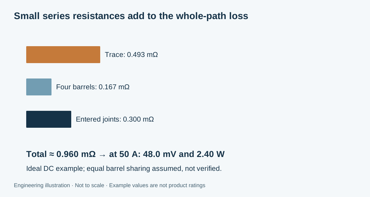
Add trace, barrel group and connection resistance
The workbench calculates a uniform rectangular trace, a group of identical cylindrical barrels in parallel and an entered series connection allowance. Every element uses the same assumed copper temperature where the copper resistivity model applies. The additional interface allowance is taken as entered. It is not independently temperature-corrected because its composition and measurement basis are unknown.
RAYPCB ENGINEERING
Heavy Copper Specifications10 oz Trace and Interconnect Loss
Loading 10 oz Trace and Interconnect Loss…
The example trace is 100 mm long, 10 mm wide and 350 µm thick at 20°C, giving 0.4926 mΩ. Each of four holes has a 0.50 mm finished inner diameter, 25 µm radial wall and 1.6 mm conducting length. Their ideal parallel resistance is approximately 0.1673 mΩ. Adding an illustrative 0.300 mΩ of other connections gives a total near 0.960 mΩ.
At 50 A, that example produces about 48.0 mV drop and 2.40 W loss. The chosen 25 µm wall is an arithmetic input, not a published 10 oz process limit or an acceptance prescription. Replace every example with the agreed or measured construction. The model's value is showing where the resistance comes from, not declaring that 50 A is safe.
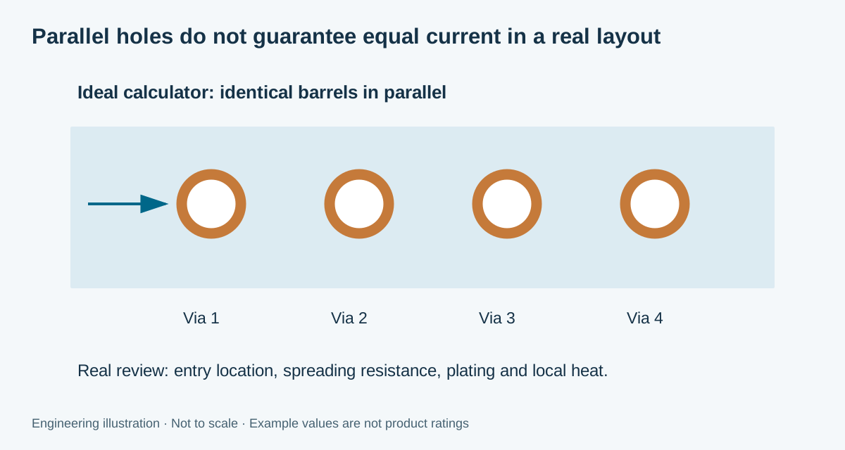
Why adding vias is not a complete current-sharing design
In the ideal model, doubling the number of identical parallel barrels halves the group's resistance. It does not halve trace resistance or the other series interfaces. A real layout also needs current to spread into each barrel. Entry location, pad geometry, copper distribution, plating variation and local temperature can make the current distribution unequal.
Do not interpret “ideal current per barrel” as an allowable current. It is total current divided by count under an equal-sharing assumption. A hole may be closer to the incoming route or connected through a narrower local feature than its neighbour. For critical designs, review the actual geometry and use appropriate electrical and thermal analysis followed by representative validation.
The tool's formula uses the conducting length of the barrel, not necessarily the complete board thickness. A connection between particular layers needs the relevant span and a model suitable for that structure. Blind, buried, filled or capped constructions can require different assumptions; do not force them into a hollow full-span model simply to obtain a number.
Review terminals, relief spokes and measurement points
High-current routes include component connections, shunts, terminals and often mechanical hardware. Make a path map showing each transition and its evidence source. A resistance allowance for a connector should not silently include the same PCB trace already calculated elsewhere. Conversely, leaving connector or joint resistance out can make the predicted voltage drop appear better than the product achieves.
Use appropriately located voltage-sense points when verifying milliohm paths. A measurement that includes test-lead or unrelated connection resistance can be mistaken for board loss. The verification method, applied current and conductor temperature should be documented alongside the result. TI's current-sensing discussion provides useful context for copper's temperature-dependent resistance.
For switching circuits, a low DC resistance does not prove that loop inductance, overshoot or EMI is controlled. Preserve the intended return path and sensing layout. The Power PCB application page considers the broader system task; this specification page does not replace topology-specific circuit design or component guidance.
Make the construction producible and inspectable
Identify copper weight and finished requirement per layer, overall thickness, minimum finished conductor geometry and the interconnect map. Review holes and resin requirements against the same construction. Separate maximum values from unrelated capability rows cannot be combined into a manufacturing promise. The real layout, material and quantity need to be assessed together.
Heavy copper also changes pad topography and assembly heat flow. Mask coverage, exposed lands, terminal holes and thermal-relief features deserve attention before assembly. A direct connection to a thick plane can affect soldering; a relief pattern can affect electrical loss. Resolve the trade-off with the assembler and the product designer, then validate a representative assembly process.
RAYPCB ENGINEERING
Heavy Copper SpecificationsHeavy Copper Construction Review Explorer
Loading Heavy Copper Construction Review Explorer…
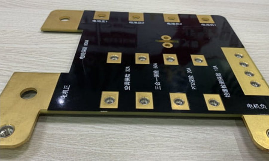
The separate 8 oz photograph is a comparison product, not evidence for a 10 oz hole or layer stack. Use drawings, material identification and appropriate inspection records to establish the actual build. IPC-6012 provides a rigid-board performance framework; record the chosen revision, class and relevant customer requirements in the order.
How interconnect requirements affect a 10 oz quotation
Two 10 oz boards of the same area may have different costs because their layer maps, holes, fine features, materials, panel use and required evidence differ. The hole-wall requirement and verification scope should be visible in the request. If a proposed change in hole count or geometry alters the design, obtain a revised quote rather than applying an assumed per-via price.
RAYPCB ENGINEERING
Heavy Copper Specifications10 oz Fabrication and Budget Brief
Loading 10 oz Fabrication and Budget Brief…
The budget brief adds only the copper-specific allowances you enter. Its construction field can identify which layers use 10 oz and which interconnect requirements remain unresolved. Blank cost fields produce a technical brief; entering only part of the cost set produces a correction request instead of quietly treating missing charges as zero.
Ask what is included in the unit price, setup and inspection allowances. The PCB quote comparison page helps align quantities, construction and acceptance scope. Exact pricing depends on a reviewed design; no per-ounce multiplier on this page represents a current factory rate.
Verify connectivity, construction and load separately
Bare-board electrical test checks the network under its agreed settings. It is different from a milliohm path measurement or a powered thermal test. A board can pass continuity while still needing product-level evaluation at the intended load. Use the PCB electrical-testing guide to separate the bare-board test task from assembly validation.
For a first build, define what cross-section, dimensional and material evidence is required and which load cases the assembled unit must demonstrate. Include the enclosure, cooling, interfaces and temperature measurement locations. IPC-2152 addresses conductor current and temperature rise; the local series-resistance calculation deliberately stops short of assigning a thermal rating.
10 oz PCB interconnect questions
Does 10 oz outer copper mean 350 µm of copper inside a hole?
No. Surface copper and radial hole-wall plating are separate requirements. The hole construction must be specified and reviewed independently.
Does doubling via count double allowable current?
Not as a general rule. The ideal model reduces barrel-group resistance, but real sharing and thermal conditions still matter. Other series elements may remain the limiting parts.
Can a filled via use the same model?
Only if its actual conductive structure matches the hollow-barrel assumptions. Filled and capped constructions need their own reviewed geometry and material model.
Is the 25 µm example an IPC minimum?
No. It is a chosen input for a worked example. Acceptance comes from the applicable specification and the approved drawing, not from the example field.
What should an enquiry include?
Send the copper map, finished thickness, hole spans and wall requirement, current path, quantity and requested evidence. State any unknown dimensions as open questions rather than guessing them.
Review my 10 oz current path
Send the layer-by-layer copper requirement, fabrication revision, geometry, quantities and required evidence. Identify open construction or load questions so engineering can review a useful manufacturing proposal.
Attach a downloaded tool brief manually. Contact does not automatically receive these inputs. References reviewed September 2026. Illustrations use planning examples; photographs do not establish prices, delivery times or project-specific acceptance.