Introduction
Printed circuit boards designed for audio applications require careful engineering to deliver quality sound performance. Audio PCBs need controlled impedances, shielding, filtering, and tight layout to maintain signal integrity.
This article provides guidance on best practices for designing analog audio PCBs, from amplifier circuits to audio codecs and digital interfaces. We’ll review layout considerations, component selection, routing techniques, and design methodologies tailored for audio. Let’s explore how to design clear, robust, and interference-free audio PCBs.
Audio Frequency Ranges
The first step is understanding the frequency ranges involved in various audio applications:
- Human hearing – Approx 20 Hz to 20 kHz max frequency range. Defines analog audio.
- Voice bandwidth – 100 Hz to 7 kHz containing most speech information.
- Hi-fi audio – High fidelity reproduction targeting 20 Hz – 20 kHz with low distortion.
- Digital audio sample rates – 44.1 kHz, 48 kHz, 96 kHz etc based on sampling theory limits.
- Control/status signals – Digital control bus speeds like I2C, SPI in the 1 MHz range.
Matching the circuit performance to the application’s frequency range is crucial.
Key Design Considerations for Audio PCBs
To achieve good signal integrity, audio PCB layouts must address:
- Impedance control – Matched 100Ω differential impedance typical.
- Low noise – Avoid crosstalk, digital interference, ground loops.
- Filtering – Low pass filter digital signals.
- Power conditioning – Clean, regulated, ripple-free power.
- Component selection – High quality capacitors, op amps, ADCs, etc.
- Grounding – Well designed grounding minimizes noise injection.
- Shielding – Isolate analog signals from interference sources.
- Board stackup – Well designed layer stack and component placement.
Paying attention in these areas ensures clarity and accuracy of the audio signal.
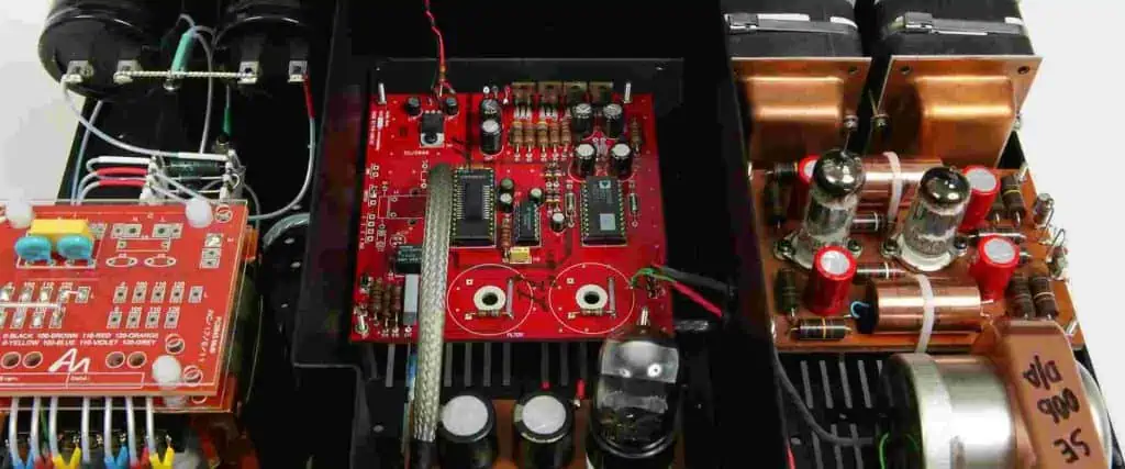
Audio Amplifier Circuit Design
Audio amplifiers boost microphone, instrument, or line level signals to drive speakers or recording equipment. Here are key amplifier PCB design considerations:
Gain Stages
- Cascaded gain stages provide required overall amplification.
- Typically 3-5 stages for heavy amplification.
- Can combine transistor and op amp stages.
Biasing
- DC biasing sets proper operating points for amplification.
- Combine resistors, feedback loops, and other bias techniques.
Feedback and Compensation
- Feedback provides impedance bridging, gain control, and compensation.
- Ensures stability for all expected circuit conditions.
Power Supply Filtering/Bypassing
- Clean steady DC supply prevents noise injection.
- metic filters, regulated design, proper decoupling.
Heat Dissipation
- Adequate cooling for heat generating components.
- Thermal design, copper fills, board mountings.
Careful analog design results in low noise and distortion.
Audio Codec, DAC, and ADC Circuits
Digital audio codecs, ADCs, and DACs translate audio signals between the analog and digital domains:
Component Selection
- High performance audio-grade converters, amplifiers, and clocks.
- Review specs like SNR, distortion, dynamic range.
Impedance Matching
- Ensure proper impedance bridging at interfaces.
- line driver amps, feedback networks.
Sampling Rate Support
- Handle typical rates like 44.1 kHz up to 192 kHz.
- Use oversampling DACs/ADCs if needed.
Filtering
- Anti-aliasing and reconstruction filters for clarity.
- MEMS microphone tuning and protection.
Port Isolation
- Separate sensitive analog and noisy digital domains.
- Digital/analog power plane splits.
Meticulous design maximizes audio resolution and dynamic range.
Digital Audio and Control Interface Design
Digital audio and control bus signal integrity also matters:
Signal Termination
- Source and load termination resistors.
- Matched trace impedance.
Interface Layout
- Keep lines short, avoid 90° angles.
- Solid ground references.
- No noisy signals routed parallel.
Board Stackup
- Route fast digital traces on inner layers.
- Reference to unbroken ground planes.
Power Decoupling
- Proper decoupling near digital ICs.
- Filter power supply inputs.
- Separate analog and digital supplies.
Care with digital interfaces prevents noise coupling into sensitive analog circuits.
Component Selection for Audio Boards
Thoughtful part selection is crucial for audio PCBs:
Audio ICs
- High quality amplifiers, codecs, converters.
- Low noise, low distortion, low crosstalk.
Passives
- 1% or better resistors, tight tolerance caps.
- Low ESR/ESL, stable temperature coefficients.
Connectors
- Gold plated contacts avoid corrosion.
- Proper pinouts.
- Secure connections.
Crystals and Clocks
- Use audio grade clock sources with low jitter.
- Ensure caps are nearby for supply filtering.
Even small component choices impact overall sound quality.
Audio PCB Layout Considerations

Paying attention to layout is vital for audio boards:
Partitioning
- Group relevant circuits together.
- Delineate separate analog and digital areas.
- Enclose sensitive analog in guards.
Impedance Control
- Tune trace geometry for target impedance.
- Reference plane layers help.
Component Placement
- Place components for short, direct connections.
- Watch for cross-talk hot spots.
Routing
- Avoid sharp corners or twisting routes.
- Use curved traces between sections.
- Keep out from ground planes.
Every layout choice affects signal integrity – tune carefully.
Shielding and Layer Stackup
Proper board layer stackup and shielding prevents interference:
Layer Usage
- Analog signals inner layers.
- Digital signals outer layers or internal power plane adjacent.
- Split power planes between analog and digital domains.
Shielding
- Use copper fills around sensitive areas.
- Careful stitching vias to connect shields.
- Spot shields around digital ICs.
Enclosure Shielding
- Seamlessly connect board shields to chassis ground.
- Prevent leakage through openings.
Shielding is the cornerstone of noise mitigation.
Audio PCB Design Process
A structured design process ensures good results:
- Define requirements – frequency range, dynamic range, distortion limits.
- Create schematic for amplifiers, converters, processors.
- Select components for low noise, high linearity.
- Develop board stackup and partition sections.
- Floorplan components and route critical connections.
- Route thoroughly, tuning impedances and shielding.
- Perform signal, power integrity, and EMI analysis.
- Review design rules and adjust layout as needed.
- Iterate until all specifications are met.
- Validate with thorough bench testing.
Care at each stage leads to a successful audio PCB implementation.
Conclusion
Designing audio PCBs requires care and expertise to maintain signal integrity and achieve high analog fidelity. Following best practices for schematic design, simulation, layout techniques, shielding, and frequency management results in boards with excellent acoustic performance. Audio circuits demand meticulous engineering and board implementation to minimize noise, interference, and distortion. A well-executed audio PCB design delivers pristine rendered sound across the entire audible spectrum.
Frequently Asked Questions
What are some typical specifications used to evaluate audio PCB performance?
Key parameters are frequency response, total harmonic distortion (THD), signal-to-noise ratio (SNR), crosstalk between channels, dynamic range, and stability across operating conditions.
What are some simple ways to start improving audio circuit layouts?
Using a clean ground plane, proper decoupling near ICs, separating noisy digital circuits from analog, keeping high speed traces short, using shielding, and minimizing crosstalk hotspots.
Why are maintaining controlled impedances important for audio PCBs?
Controlled impedances like 100Ω differential for clock and audio signal traces prevent signal quality degradation due to reflections and standing waves that cause ringing and distortion.
How can I check an audio PCB design for susceptibility to EMI issues?
Performing appropriate susceptibility simulations, scanning near field probes across the operating board, or testing in a semi-anechoic chamber can reveal emitted or received EMI/RFI issues. Shielding and filtering can then help mitigate observed problems.
What are some audio-specific integrated circuits used in audio PCB design?
High performance audio amplifiers, audio codecs for A/D and D/A conversion, digital signal processors and effects chips, microphone preamplifiers, high resolution ADCs/DACs, and audio-specific microcontrollers.
For printed circuit board design engineers, phones give a definitive test. Every subsystem has conflicting necessities, and current phones incorporate virtually every subsystem found in a compact gadget. An excellent audio PCB must amplify the exhibition of every gadget connected with it and keep the different subsystems from meddling with one another. The conflicting necessities of every subsystem bring about some trade-off. At last, even though the importance of audio in mobile phones is expanding, the audio circuit board is regularly given minimal thought during its pcb layout.

Segment Placement
The initial step of any audio PCB configuration is picking where to put the parts. Careful segment position can ease ground partitioning and signal routing. It limits noise pickup and the audio circuit board required.
The RF part of a phone is regularly viewed as simple. However, there is a typical issue in numerous mobile phone plans where noise coupled from the RF segment into the sound hardware is demodulated into discernible noise. To forestall this, the RF and sound segments should be isolated, however much as could reasonably be expected.
PDAs contain a combination of analog and digital hardware that should be isolated to keep noise from the computerized parcel from meddling with the delicate, simple circuits. Apportioning the audio PCB into an analog and a digital area improves the partition task.
When the audio PCB has been parceled into RF, digital and analog regions, the part arrangement inside the simple segment should be chosen. Segments ought to be set to limit the distance that sound signs travel. Find the amplifier circuit board near the loudspeaker and headphone jack. This placement will limit EMI radiation from Class D speaker enhancers and limit the noise defenselessness of low-sufficiency earphone signals. Put the gadgets providing the simple sound near the enhancer as conceivable to limit noise pickup on the intensifier inputs. All information signal follows will go about as antennas to RF signals. However, reducing the traces decreases the radio wire productivity for frequencies regularly of concern.
Audio circuit board Design Tips

Designing audio PCB stays a test, and parts of it usually are thought about somewhat of a professional. Indeed, even the best creators frequently need to assemble more than a circuit board to deliver a tremendous noise-free plan. The following are a few hints from our encounters:
OpAmp Circuits
Fast OpAmps are not helpful for sound. There are several issues with gadgets like the LMV722, a 10MHz OpAmp wavering fiercely when utilized with computerized pots that add a touch of propagation deferral to the criticism resistor—changing to an LMV358 which is a 1MHz OpAmp address the issue.
When planning an op amplifier circuit board, you frequently discover you need to alter a sound signal to accomplish the least complicated circuit. It is fine and is just an issue where you have one signal rearranged and another not as this would make them be out of the stage when heard.
Capacitors
Sound sign series capacitors: –
You can use them anywhere if you want to segregate segments from one another. Qualities to utilize: – 100nF is fine 220nF is typical if you need to lessen cost/size, best not to go beneath 100nF.
Try not to utilize ceramic/clay capacitors. The explanation is that fired capacitors will give a piezoelectric impact to an AC signal which causes noise. Utilize a Poly of some kind – Polypropylene is best; however, any will do. It is reasonable for high purity applications, not a general standard sound plan.
Try not to utilize tantalum capacitors anyplace inside sound sign ways (a few originators may differ; however, they can cause ghastly issues). A by and largely acknowledged substitute for polycarbonate is PPS (Polyphenylene Sulfide).
Interfacing
When interfacing with other hardware, if controlling some different PCBs that incorporate sound hardware guarantee, there is just one point where GND associates between the two boards ought to in a perfect world be at the sound simple sign association point. Would you control the other board utilizing a gliding supply and connect GND without supply power through it? To signal IO associations with different gadgets or to the rest of the world, it is a decent idea to utilize a 100R resistor between GND circuits and the rest of the world GND for everything to stop ground circles made.
Signal
Where conceivable, stay away from in and out the sound signal to and from IC‘s running in equal on the PCB as this can cause motions, which feed on output to input. Keep in mind that simply 5mV can cause a lot of noise. Keep digital ground planes from sound GND and sound hardware by and large. Noise can be brought into sound just from tracks being too close to advanced planes.
Grounding
Grounding is essential in deciding if the framework accomplishes the gadget’s latent capacity. An inadequately grounded framework will probably have high RF susceptibility, crosstalk, noise, and distortion. Albeit one can address how long ought to be committed to framework grounding, a painstakingly planned establishing plan keeps several issues from happening.
The ground in any framework should fill two needs. To start with, it is the return way for all flows streaming to a gadget. Second, it is the reference voltage for both analog and digital circuits. Grounding would be a straightforward exercise if the voltage at all marks of the ground could be similar. All traces and wires have a limited obstruction. It implies that there will be a relating voltage drop at whatever point there is current moving through the ground. Any circle of wire additionally frames an inductor. It implies that at whatever point current streams from the battery to a heap and back to the battery, the current way has some inductance. The inductance builds the ground impedance at high frequencies.
While planning the best ground framework for a specific application is no basic assignment, some broad rules do make a difference to all frameworks.
- Flood All Unused PCB Area with Ground: At whatever point two bits of copper run close to one another, a little capacitive coupling is shaped between them. By running ground flood close signal traces, undesirable high-recurrence energy in the sign lines can be shunted to the ground through the capacitive coupling.
- Maximize the Effectiveness of Bypass Capacitors: Virtually all gadgets require to sidestep capacitors to give immediate current. Find these capacitors as close as conceivable to the inventory pin, which they are bypassing if you want to reduce the capacitor inductance. Any inductance diminishes the viability of the detour capacitor. Likewise, the capacitor should be given a low-impedance association with the ground to limit the capacitor’s high-recurrence impedance. Straightforwardly interface the ground side of the capacitor to the ground plane instead of directing it as anything but a trace.
- Use the Star Grounding Technique for Analog Circuits: Star grounding utilizes a solitary point on the PCB as the main ground point. This point, and just this point, can be viewed as a ground potential. In a wireless device, the battery ground terminal is a legitimate selection for the star point. Try not to consider currents streaming into the ground plane and vanishing; instead, consider all ground currents streaming back to this ground point.
In general, the audio amplifier circuit board will draw a moderately huge current that can unfavorably influence both their own and other ground references in the framework. To forestall this issue, give committed return ways to spanned enhancer power grounds, and earphone jack ground returns. Segregation permits these flows to stream back to the battery without influencing the voltage of different pieces of the ground plane. Keep in mind that these devoted return ways should not be directed under digital signals because they could hinder the computerized bring flows back.
- Keep Ground Currents Separate: Separate the ground current on analog and digital circuits to keep digital current from adding noise and radiation to the analog circuits. An ideal approach to achieve this is through the right segment situation. If every analog and digital circuit is set on independent pieces of the PCB, the ground traces will usually be secluded. For everything to fall into place well, the simple segment should contain just simple circuits on all PCB layers.
- Establish a Continuous Ground Plane for Digital Circuits: Digital current will follow the direction of the signal. It makes the littlest circle region for the current, accordingly limiting the antenna’s inductance and effects. An ideal approach to guarantee that all digital signal traces have a comparing ground way is to build up a ceaseless ground plane quickly contiguous the signal layer. This layer should cover a similar region as the computerized signal follow and have a couple of breaks in its progression as could be expected. All breaks in the ground plane, including vias, prompt the ground current to stream in a bigger circle than ideal, expanding noise and radiation.
The advantage of audio amplifier PCB board
• It has a more noteworthy recurrence than the others. You would need to depend on radio recurrence exercises to accomplish 80% unwavering quality with these intensifiers.
• This is alluded to as an elective arrangement since the Amplifier can eliminate cross-over noise.
• These gadgets transfer half of a half-wave, bringing about a total current to drive the load. As a result, the speaker PCB is more successful.
• It is considered to have an improved power quality and feedback loop. They are additionally easy to assemble, with only one unit and few sections.
Downsides of audio amplifier PCB board
• This is so even though they have an excellent altercation of their scores. It happens regularly with enhancers since the PCB will create a more noteworthy current.
• The yield gadgets would undoubtedly get hot if overheating is not overseen by effectively fitted warmth sinks.
• This activity can damage portions of the PCB or obliterate the PCB structure.
• There are times that PCB follows are introduced mistakenly. It requires standard patching during the evacuation and substitution of yield parts.
Conclusion
Although making an all-around audio PCB can be tedious and testing, the venture is worth the time spent. The final product is a framework with less noise, higher insusceptibility to RF signals, and less impedance. The audio circuit board will likewise have better EMI execution and may require less protection.
At last, if the audio PCB is not painstakingly planned, preventable issues will be found when the item is in the test. These issues are substantially harder to fix once the design is finished and regularly request critical chances to address. All around regularly, the fixes require extra segments that add to the all-out framework cost and intricacy.