Introduction
PCB assembly or PCBA refers to the manufacturing process where electronic components are mounted and soldered onto a printed circuit board to realize an electronic device or system. Implementing an optimized PCBA design flow is crucial for assembling PCBs that meet all functionality, reliability and quality requirements cost-effectively.
This guide provides a comprehensive overview of best practices and key considerations across the PCBA design stages:
- Component selection
- PCB footprint design
- Placement considerations
- Routing
- Thermal design
- Post-assembly inspection
- Manufacturing guidelines
Following these PCBA design principles and strategies will help achieve optimized manufacturability, yield and performance.
Component Selection
Choosing the right components is the first step in PCBA design. Key guidelines for component selection are:
- Functionality – Components must meet all technical specifications in terms of functionality, electrical ratings, tolerance, frequency response etc.
- Availability – Select industry standard components that will be available through multiple suppliers and long lifetime.
- Cost – Balance performance needs with component costs and pricing trends. Consider lower cost equivalents.
- Supplier – Prefer reputable authorized suppliers over unknown third-party component vendors.
- Packaging – Give preference to surface mount packages for ease of assembly. Avoid outdated leaded packages.
- Lifecycle – Choose components that are not nearing end-of-life status or select alternate replacements.
- Counterfeits – Insist on parts from authorized distributors to avoid fake components.
- Environment – Select RoHS compliant lead-free components suited to the operating environment.
- Parametric Search – Leverage vendor component databases like Digikey, Mouser for parametric searching.
Careful component selection right at the design stage sets the foundation for a smooth PCBA process.
PCB Footprint Design

The PCB footprint or land pattern refers to the copper pads and traces on the board providing the electrical and mechanical interface for soldering components. Good footprint design ensures reliable solder joints. Key aspects:
- Datasheet recommendations – Follow datasheet specifications for pad dimensions, layout and thermal reliefs.
- Package type – Tailor footprint layout for the component package – QFP, SOP, BGA etc.
- Dimensioning – Account for factors like mask alignment tolerance, solder mask expansion, hole drilling accuracy.
- Pad shape and size – Appropriate for leads or balls, allow for tolerances and solder coating.
- Paste masks – Define suitable solder paste areas for formation of correct joints.
- Thermal relief – Include ground plane cutouts under pads for heat dissipation during soldering.
- Annular rings – Ensure recommended pad overlap with drill holes to avoid tombstoning.
Poor footprint design can lead to issues like open circuits, shorts, distorted solder joints and failed boards. Matching PCB footprints to component packages is essential.
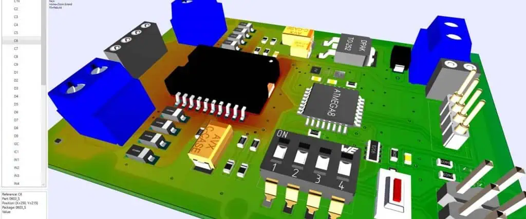
Component Placement
Optimal component placement lays the foundation for efficient PCB routing by minimizing track lengths and allowing routing completion. Guidelines for effective placement include:
- Circuit topology – Place connected components close with minimal connections between clusters.
- High pin count ICs – Position to allow shortest routes to related sections.
- Thermals – Separate heat generating parts with sufficient clearance for ventilation and cooling.
- Decoupling – Place decoupling capacitors adjacent to each IC power pin.
- Matching components – Group components like resistors and capacitors together for consistency.
- Symmetry – Arrange sections symmetrically for ease of routing and assembly.
- Manual vs auto-place – Use strategic manual placement before optimizing with auto-placers.
- Density – High component density increases manufacturing difficulty and cost.
- Assembly – Ensure adequate space for soldering and inspection access.
- Testpoints – Include testpoints at key nodes for debugging and troubleshooting.
- Form factor – Consider the housing and required external connectivity.
An adaptable placement with optimal grouping of components avoids routing congestion and minimizes re-spins.
Routing Considerations
Routing creates the interconnect copper traces between pins and terminals to complete the electrical connections in the PCB based on the placement. Key routing tips:
- Trace width – Size traces based on current levels and temperature rise.
- Via – Minimize vias for better signal quality. Use stacked/filled vias where needed.
- Signal integrity – Use impedance matching, controlled routing layers, and termination for high-speed signals.
- Cross-talk – Provide adequate isolation between noisy digital and noise-sensitive analog signals.
- Split power and ground planes – Use separate ground layers for analog and digital sections to avoid digital noise coupling.
- Decoupling – Include decoupling capacitors across power nets with very short connections.
- Supply data – Clearly specify all supply rails including voltage levels on the schematics.
- Alignment – Maintain alignment between routes on adjacent layers for optimal layer transitions.
- Manufacturability – Account for fabrication limitations in trace/space and hole size.
- Testability – Include testpoints to access internal buses and signals for testing.
- EMI – Control radiation using shielded enclosures and internal ground planes.
Applying appropriate routing practices ultimately results in functionally complete PCBs meeting signal quality needs.
Thermal Design
Careful thermal management is vital for ensuring components operate safely within their temperature limits. Effective thermal design involves:
- Heat sinks – Use heat sinks over hot components like linear regulators and power transistors.
- Vias – Place thermal vias beneath hot parts connecting to ground planes to conduct heat.
- Fans/blowers – Forced air cooling through fans, blowers to remove heat in high power boards.
- Metal cores – Use thick metal core PCBs for enhanced heat spreading in extreme environments.
- Clearances – Ensure sufficient clearances around sensitive ICs for air flow and ventilation.
- Thermal analysis – Perform thermal simulation and analysis to identify hot zones and spreading.
- Thermal camera – Use IR thermal cameras to visualize board heating during operation.
- Thermal throttling – Implement power throttling and shutdown in firmware to prevent overheating.
- Component ratings – Check ratings and limits before derating high power parts.
- Heaters – Consider self-heating components to maintain minimum temperature in cold environments.
Adequate thermal design prevents component damage, intermittent problems and system failures in demanding operating environments.
Post-Assembly Inspection
Post-assembly validation tests screen for manufacturing defects before firmware testing. Important checks include:
Visual Inspection
- Component placement
- Solder joint quality
- Physical damage
Electrical Tests
- Power sequencing
- Supply voltage levels
- Ground integrity
- Basic connectivity
Function Tests
- Clock signals presence
- Reset operation
- GPIO inputs and outputs
Burn-in Testing
- Prolonged thermal and voltage stress screening
X-ray Imaging
- BGA/CSP solder joint inspection
Bed of Nails
- Pin-level correctness testing
Flying Probe
- Testing without fixturing for fast debugging
Executing a suite of inspection tests after PCBA manufacturing eliminates assembly issues before final equipment integration and test.
Design for Manufacturing
Adhering to design for manufacturing guidelines ensures that PCBs can be assembled easily at optimal cost:
- Component Selection – Prefer surface mount over leaded parts; avoid obsolete packages.
- Footprint – Follow datasheet specifications; allow tolerances.
- Placement – Enable both side assembly with clearance for tool access.
- Rotate parts – Rotate polarized capacitors, diodes and ICs for accessibility.
- Annular rings – Maintain adequate annular rings around drilled holes.
- Spacing – Provide sufficient spacing between parts and copper for soldering.
- Thermals – Include thermal reliefs in pads for soldering heat dissipation.
- Traces – Use appropriate trace widths based on current; allow for tolerances.
- Vias – Minimize unnecessary vias; enable filled, plugged and blind/buried vias.
- Layers – Maintain symmetry across layers; clearly define lamination sequence.
- Markings – Specify reference designators, polarity indicators, board outline.
- Testpoints – Include accessible testpoints for validation and troubleshooting.
Electronics manufacturing services can provide expert guidance on design refinements needed to enhance manufacturing process performance.
Conclusion
A robust PCBA implementation requires extensive upfront planning and design effort. Following the guidelines across component selection, footprint design, placement planning, routing, thermal management and post-assembly inspection stages of PCBA enables assembling boards that deliver the required functionality, quality and reliability in a cost-optimized manner. A successfully executed PCBA process is key to developing electronic products with faster time-to-market.
PCB Assembly Design Guide – FQA

Q1. What is the importance of component placement in PCBA design?
Effective component placement minimizes interconnect lengths, reduces crosstalk, allows simpler routing and improves overall manufacturability. It is a crucial step impacting cost, performance and reliability.
Q2. What are some considerations for routing a PCB?
Key routing considerations are signal integrity, impedance matching, cross-talk avoidance, decoupling, power planes, trace widths, vias minimization, testability, manufacturability and EMI control through careful layout.
Q3. How is thermal management incorporated in a PCBA design?
Methods for thermal management in PCB assembly include heat sinks, thermal vias, fans, blowers, metal core PCBs, adequate clearances, thermal simulation analysis and thermal camera inspection.
Q4. What post-assembly validation tests help screen manufacturing defects?
Post-PCBA validation tests include visual inspection, electrical tests, functional tests, burn-in, x-ray, bed-of-nails, and flying probe. This eliminates assembly issues before integration.
Q5. What are some PCB design guidelines for optimizing manufacturability?
Design for manufacturing guidelines include component selection, footprints, placement, spacing, annular rings, trace widths, layer management, testpoints and assembly markings on PCB layout.