
RAYPCB · ENGINEERING GUIDE
Analog PCB Design: Control Return Paths, Noise and Settling
Analog PCB design preserves the useful signal while controlling the errors added by its source, circuit, layout and measurement. A schematic with accurate component values can still perform poorly if return currents, reference connections, thermal gradients or sampling behavior are overlooked. Begin with the signal range and error budget before choosing a universal ground rule.
This page focuses on physical implementation and a first-order RC calculation. The worksheet calculates the time constant, cutoff frequency and ideal step-settling time from entered values. It is an unloaded single-pole model, not a simulator for an amplifier, switched-capacitor ADC or complete acquisition channel. For endpoint gain and offset planning, use the separate signal-conditioner guide.
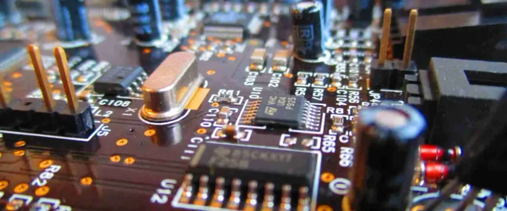
Turn accuracy into an error budget
Write the required input range, bandwidth, source impedance and smallest meaningful change. Then state the allowed error at the point where the result is used. Resolution, repeatability, absolute accuracy and noise are different quantities; a high-resolution converter does not by itself guarantee an accurate product measurement.
Allocate errors to the sensor or source, input protection, gain, reference, conversion and calibration. Some errors behave as offsets, others scale with input and others vary with temperature or time. Keep their treatment explicit rather than summing every typical datasheet number as though it were a guaranteed worst-case bound.
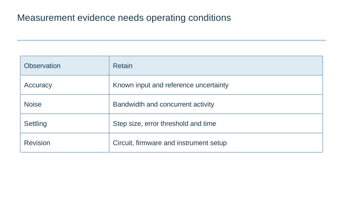
Choose an observable test for each important allocation. A quiet input test can reveal output variation, while a known input sweep exposes gain and nonlinearity. Record the instrument configuration and expected uncertainty. Otherwise the test equipment or connection can obscure the improvement the board revision was supposed to make.
Analog problems require different observations
| Question | Useful evidence | What it cannot establish |
|---|---|---|
| DC accuracy | Known input with defined reference uncertainty. | Wideband noise or fast settling. |
| Noise | Bandwidth-limited record with operating activity identified. | Absolute gain and offset accuracy. |
| Settling | Step size, residual-error threshold and timing. | Behavior for all loads and input sequences. |
| Coupling | Correlated activity and measurements along the path. | A universal ground-plane rule. |
Trace the return path before splitting planes
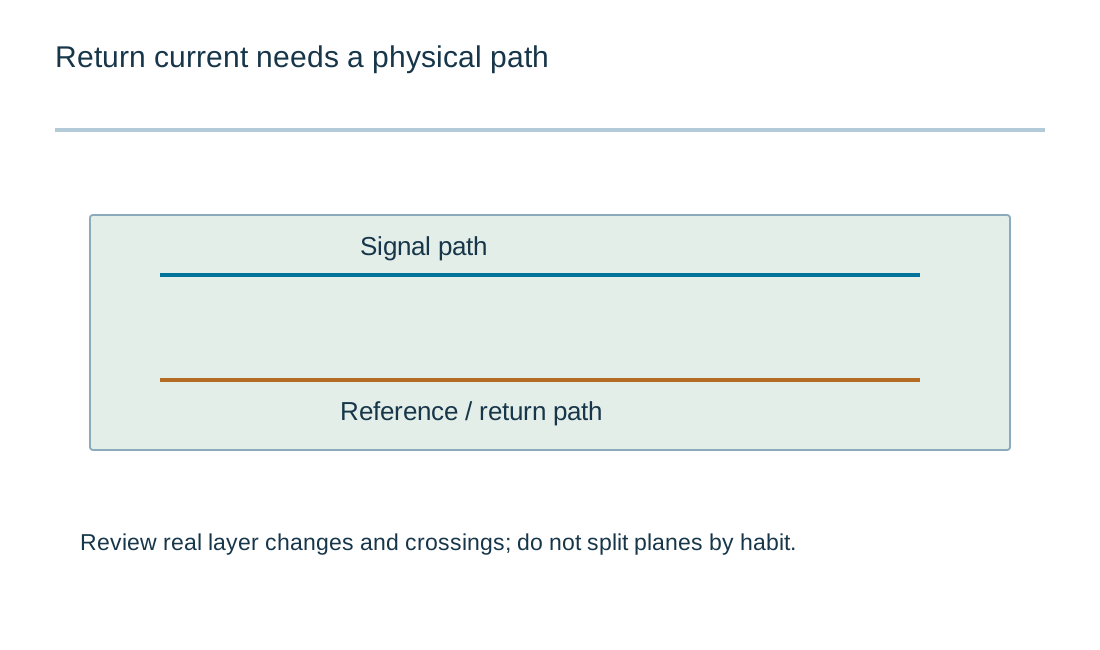
Mark where each relevant current returns, including clocks, digital interfaces, converter switching currents and external connections. Placement should help keep unwanted currents away from sensitive measurement paths. Naming two nets analog ground and digital ground does not explain how current crosses the physical board.
A continuous reference structure can be appropriate for many mixed-signal designs; automatically cutting a plane can force signals to take an undesirable return path. Conversely, actual isolation or a documented circuit architecture may require a deliberate separation. Follow the selected components and system boundary rather than applying either approach as a slogan.
The Analog Devices grounding discussion is useful for reasoning about current paths. Apply that reasoning to the actual layer stack and signal routing. Review every signal that changes layers or crosses between functional regions, including its reference continuity, rather than judging the board only from the top-layer appearance.
| Review item | What to establish |
|---|---|
| Signal requirement | Range, bandwidth, source impedance and allowed error at the output. |
| Return paths | Physical reference structure and currents near sensitive nodes. |
| RC assumptions | Unloaded single pole; effective R/C and step-error definition. |
| Real load | Driver stability, ADC sampling and multiplexed settling reviewed separately. |
| Test evidence | Known input, operating activity, probe setup and calibration scope. |
First-order RC cutoff and settling
First-order RC cutoff and settling
Use the current inputs and keep the assumptions
Load the example to learn the worksheet, then clear it before entering your project values. Blank fields are not silently converted to zero. Units and selected conventions belong to the result, so review them together with the numbers. Editing any input invalidates the previous result and disables its download until you calculate again. Edited example data remain labeled as an illustrative example.
This tool runs locally on the values you enter. It does not open a schematic, select approved components, measure signals or inspect a physical board. Keep the exact component documents and a record of measurements with the design. Downloading the text report does not send an enquiry or populate the Contact form. Attach it manually if it helps explain a specific engineering question; completing the worksheet is optional.
| Input | What to establish before using it |
|---|---|
| Review reference | Use a nonconfidential revision reference. |
| Series resistance · Ω | Source resistance and loading are excluded unless incorporated deliberately. |
| Shunt capacitance · nF | Use appropriate effective capacitance, not merely nominal marking. |
| Remaining step error · % | Strictly between 0 and 100; this is a settling fraction, not a total accuracy budget. |
Use the RC worksheet with the right boundary
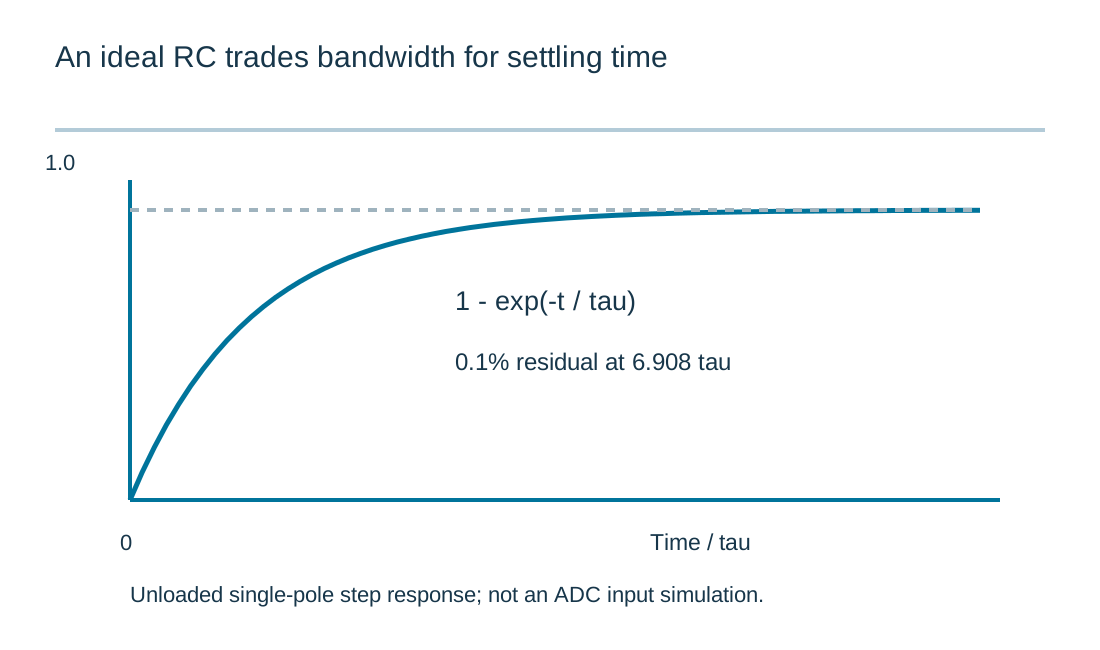
The model assumes a resistor feeding a capacitor, an ideal step source and an unloaded output. It reports tau equals R times C and the single-pole cutoff of one divided by two pi R C. Settling to an entered residual fraction uses minus tau times the natural logarithm of that fraction.
For the teaching example, 1 kilohm and 100 nanofarads give a 100-microsecond time constant and approximately 1591.5 Hz cutoff. Reaching 0.1 percent residual error takes about 690.8 microseconds in this ideal model. Those values explain the bandwidth-versus-settling tradeoff; they are not an ADC input-network recommendation.
Check the effective source resistance and output loading before using the result. Component tolerance and effective capacitance can shift both bandwidth and settling. If the load samples charge, an amplifier is involved or the input is multiplexed, the real response needs additional analysis. Do not treat a single exponential as proof of acquisition accuracy.
Place the reference and sensitive nodes deliberately
Identify the nodes whose small disturbances directly affect the result: high-impedance inputs, reference inputs, feedback nodes and differential measurement connections. Keep their paths purposeful and avoid unnecessary branches, probes or adjacent aggressors. The relevant distance depends on the circuit; this page does not prescribe one spacing for every analog board.
Treat the reference as a signal path with its own loading and return behavior. Check the converter manufacturer's decoupling and connection guidance, and keep the reference arrangement consistent with the intended measurement. A precision reference part cannot compensate for an uncontrolled voltage drop in its connection to the converter.
Review leakage and contamination sensitivity where high impedance makes them significant. Assembly materials, cleaning choices and handling can matter to these circuits. State those requirements in the assembly documentation instead of expecting the manufacturer to infer them from a component value or a small gap on the drawing.
Keep switching and digital activity in the test scenario
Measure the analog channel while the rest of the product performs representative work. A quiet bench mode may omit radio bursts, processor activity, display updates or converter load steps. Correlate disturbances with those events before changing the analog circuit at random.
For a suspected power interaction, review the regulator placement and loss guide. For a digital sensor connection, the sensor-board pull-up worksheet addresses a different electrical question. Neither tool measures noise coupling, but each can make a relevant assumption visible in the investigation.
Keep probe technique consistent. Probe loading, ground connections and instrument bandwidth influence what appears on the display. Record how the measurement was made, not merely the number reported. A screenshot without the operating condition and connection point is difficult for another engineer to interpret.
Prepare layout review and assembly evidence
Review the schematic, placement, stackup and routing together. For each critical path, identify the source, destination, return, reference and adjacent disturbance source. Ask what happens during startup or partial power as well as during normal conversion. An input that is acceptable during operation may need protection under another sequence.
Define the calibration and functional-test scope before ordering the assemblies. State whether the build requires only electrical continuity, programming, a known input response, a calibration procedure or retained calibration data. These activities produce different evidence and should not be combined under an undefined tested label.
When contacting RAYPCB, provide the current release and a focused question: for example, a sensitive-node process requirement or the practicality of the planned test access. Include the relevant accuracy or handling requirement without expecting a general manufacturing review to certify the complete analog performance. A clear boundary between design intent and manufacturing evidence makes the next revision easier to trust.
Keep the measurement chain and its evidence together
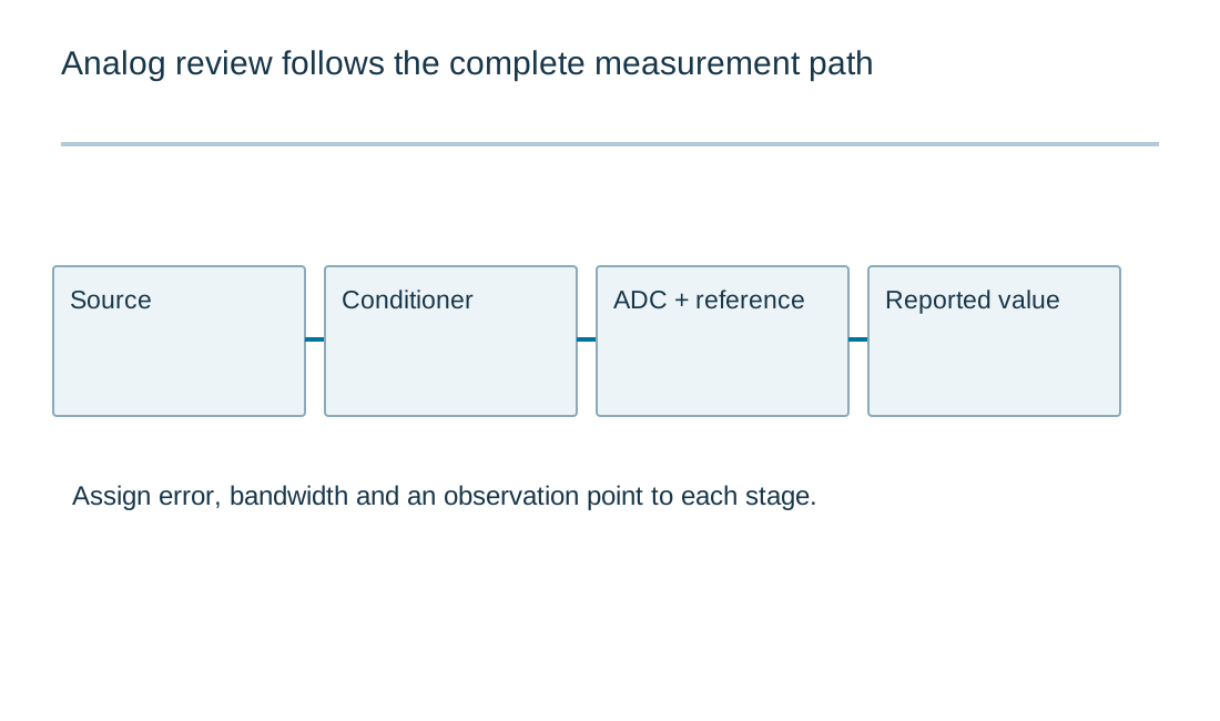
Identify the physical input, electrical source, conditioning stage, converter reference, digital representation and final reported quantity. Give each stage a requirement and a way to observe its behavior. This helps distinguish a real change in the measured quantity from an error introduced by the circuit, its environment or software interpretation.
Define the conditions for a meaningful comparison: input stimulus, bandwidth, supply state, relevant product activity, instrument connection and revision. An average value can hide an intermittent disturbance, while a single peak can be misleading without its time scale and operating condition. Keep raw evidence and processing assumptions distinguishable. Calculators on this page support a bounded part of the reasoning; they do not measure the system or replace the selected components' requirements and representative hardware tests.
Standards, source context and limits
The referenced manufacturer documentation supports specific devices, interfaces or design methods. Apply the version and operating conditions appropriate to the actual part. A similar product name is not evidence that pin functions, voltage tolerance, startup behavior or package dimensions match. Worked examples illustrate reasoning and arithmetic; they are not released schematics or independent hardware test results.
For fabrication scope and the agreed construction requirements, see PCB manufacturing.