Designing 8-Layer VR Wearable Glasses Rigid-Flex PCB
Virtual Reality (VR) wearable glasses require compact, lightweight, and high-performance electronics. An 8-layer Rigid-Flex PCB design offers the ideal solution, combining the benefits of rigid boards with the flexibility needed for compact, ergonomic designs. This guide will walk you through the process of designing such a PCB for VR glasses.
Understanding the Requirements
VR glasses typically need:
- High-speed digital circuits for video processing
- Analog circuits for sensors and power management
- RF circuits for wireless connectivity
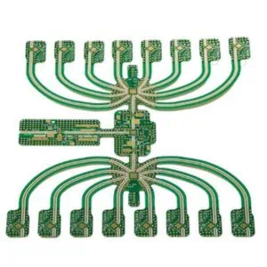
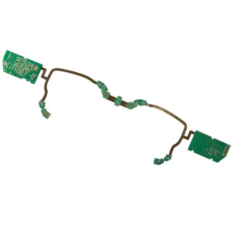
- Flexible sections to fit into the glasses frame
Layer Stack-up
A typical 8-layer stack-up for VR glasses might look like this:
- Top Layer: Components and high-speed signals
- Ground Plane
- Power Plane
- Signal Layer 1
- Signal Layer 2
- Ground Plane
- Power Plane
- Bottom Layer: Components and additional routing
The flexible sections will typically use a subset of these layers, often 2-4 layers.
Design Considerations
1. Partitioning
Divide your design into functional blocks:
- Display driver section
- Sensor integration (e.g., accelerometers, gyroscopes)
- Power management
- Wireless communication (e.g., Wi-Fi, Bluetooth)
- Audio processing
Place these blocks strategically to minimize interference and optimize signal integrity.
2. High-Speed Design
- Use controlled impedance traces for high-speed signals
- Implement differential pairs for critical high-speed lines
- Maintain signal integrity with proper termination techniques
- Use ground planes and vias for shielding and return paths
3. Flex Sections
- Design flex sections to accommodate the glasses frame geometry
- Use hatched ground planes in flex areas to improve flexibility
- Avoid sharp bends; use gradual curves instead
- Place components away from bend areas
4. Power Distribution
- Use separate power planes for digital and analog circuits
- Implement low-noise power distribution for sensitive circuits
- Consider using embedded capacitors for improved decoupling
5. Thermal Management
- Use thermal vias under high-power components
- Consider copper coin technology for enhanced heat dissipation
- Implement thermal simulation to identify and address hotspots
6. EMI/EMC Considerations
- Use proper grounding and shielding techniques
- Implement EMI suppression components strategically
- Consider using buried capacitance for improved EMI performance
Design Process
- Schematic Design:
- Create a detailed schematic capturing all components and connections
- Define power domains and ground references
- Specify critical nets and differential pairs
- Component Placement:
- Place components logically based on functional blocks
- Consider signal flow and minimize trace lengths
- Ensure adequate spacing for assembly and rework
- Stack-up Design:
- Work with your PCB manufacturer to define the layer stack-up
- Ensure proper impedance control for high-speed signals
- Define flex and rigid sections
- Routing:
- Route critical signals first (clocks, high-speed data lines)
- Use appropriate trace widths and spacing for different signal types
- Implement proper via usage (e.g., micro vias for dense areas)
- Power Distribution:
- Design power and ground planes
- Implement proper decoupling capacitor placement
- Consider using embedded planar capacitance
- Flex Circuit Design:
- Define flex circuit outline and bend areas
- Route signals perpendicular to bend lines where possible
- Use teardrop reinforcement at pad connections
- Signal Integrity Analysis:
- Perform impedance calculations
- Run signal integrity simulations for critical nets
- Adjust design based on simulation results
- EMI/EMC Design:
- Implement proper shielding techniques
- Use EMI suppression components as needed
- Consider board edge termination techniques
- Thermal Analysis:
- Perform thermal simulations
- Adjust component placement or add thermal management features as needed
- Design Rule Check (DRC):
- Run comprehensive DRC to ensure manufacturability
- Address any violations or obtain necessary manufacturer approvals
- Documentation:
- Create detailed fabrication and assembly drawings
- Specify special requirements for flex sections and VR-specific features
Advanced Techniques
- Optical Integration:
- Consider integrating optical elements directly onto the PCB
- Design for precise alignment of display components
- 3D Design:
- Use 3D PCB design tools to ensure proper fit within the glasses frame
- Consider flex-to-install requirements for final assembly
- Miniaturization:
- Utilize advanced packaging technologies (e.g., chip-scale packages)
- Consider embedded components for further size reduction
- Sensor Integration:
- Design for precise placement and orientation of motion sensors
- Implement proper isolation for sensitive analog circuits
- Wireless Performance:
- Optimize antenna placement and design
- Consider using the PCB itself as part of the antenna structure
Conclusion
Designing an 8-layer Rigid-Flex PCB for VR wearable glasses is a complex task that requires careful consideration of various factors. By following these guidelines and working closely with your PCB manufacturer and assembly house, you can create a high-performance, compact, and reliable design suitable for next-generation VR glasses. Remember to iterate and refine your design based on prototyping and testing results to achieve optimal performance and user experience.