-
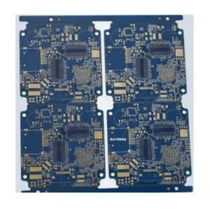
Layer Stack-up:
- The PCB consists of 6 layers, as shown in the diagram.
- Typically, layers 1 and 6 (top and bottom) are used for components and signal routing.
- Inner layers (2-5) are often used for power planes, ground planes, and additional signal routing.

-
Blind Vias:
- Blind vias connect an outer layer to one or more inner layers, but not through the entire board.
- In the diagram, you can see examples of blind vias connecting various layers (1-2, 1-3, 2-4, 3-5, 4-6).
- These vias allow for higher density routing and improved signal integrity.
-
Material Considerations:
- For millimeter wave applications, low-loss materials are crucial.
- Common materials include Rogers RO4350B or RO3003, which offer low dielectric loss at high frequencies.
-
Impedance Control:
- Precise impedance control is critical for millimeter wave circuits.
- Typically, 50 Ohm impedance is maintained for signal traces.
- The width of traces and the distance between layers are carefully calculated to achieve the desired impedance.
-
High-Frequency Considerations:
- Millimeter wave frequencies (typically 30 GHz to 300 GHz) require special design considerations.
- Minimize trace lengths to reduce signal loss.
- Use of microstrip and stripline transmission line structures.
- Careful via placement to minimize parasitic effects.
-
EMI/EMC:
- Proper shielding and grounding are crucial to minimize electromagnetic interference.
- Ground planes and vias are strategically placed to create effective Faraday cages around sensitive circuits.
-
Thermal Management:
- High-frequency circuits can generate significant heat.
- Thermal vias may be used to conduct heat away from critical components.
-
Manufacturing Challenges:
- Tight tolerances are required for millimeter wave PCBs.
- Blind vias add complexity to the manufacturing process.
- Specialized equipment and expertise are needed for proper fabrication and testing.
-
Component Placement:
- Critical components like antennas, amplifiers, and mixers need careful placement.
- Keep high-frequency sections isolated from digital or low-frequency sections.
-
Testing and Verification:
- Special test equipment like Vector Network Analyzers (VNAs) are used for testing.
- Time Domain Reflectometry (TDR) may be employed to verify impedance consistency.

This type of PCB design requires advanced knowledge of high-frequency circuit design, electromagnetic theory, and PCB manufacturing processes. It’s often used in applications such as automotive radar, 5G communication systems, and industrial sensing.