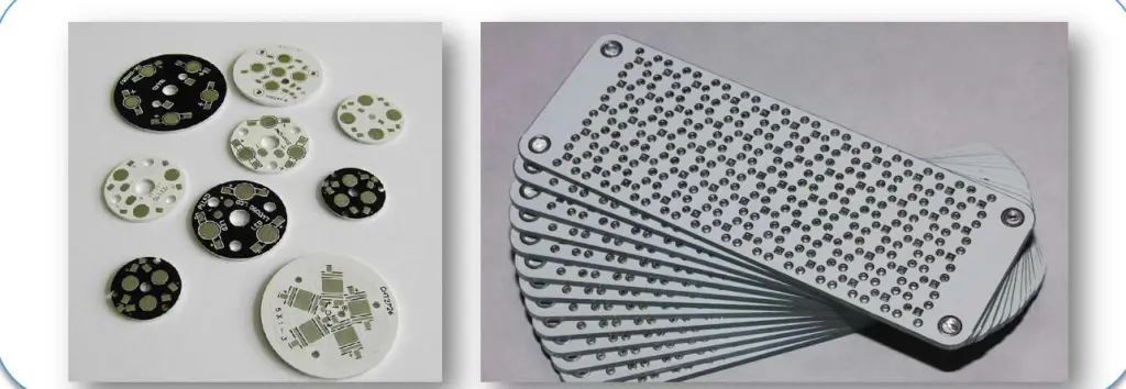
In recent years, the demand for aluminum PCBs has surged due to their numerous advantages over traditional FR4 PCBs. Aluminum PCBs are lightweight, highly conductive, and capable of withstanding high temperatures, making them ideal for applications in aerospace, automotive, LED lighting, and beyond.
This comprehensive guide will take you through the aluminum PCB manufacturing process step by step. We’ll explore the fabrication of single-layer, double-layer, and multilayer aluminum PCBs, providing a detailed look at how our engineers create these specialized boards. By the end, you’ll have a clear understanding of the entire process.
At RAYMING, we bring deep expertise in aluminum PCB manufacturing. Our state-of-the-art factory in China produces all types of aluminum PCBs, adhering to strict quality control and inspection protocols at every stage. With optimized fabrication techniques, we ensure high yields, fast turnaround times, and consistently flawless results.
Learn more about:
- PCB Manufacuring Process
- Rigid Flex PCB Manufacturing Process
- Flex PCB Manufacturing Process
- Flex PCB Assembly
- Rigid Flex PCB Assembly
Understanding Aluminum PCBs

Before diving into the manufacturing process, let’s understand what makes aluminum PCBs special.
What Are Aluminum PCBs?
Aluminum PCBs are circuit boards that use an aluminum base as the substrate instead of the traditional FR-4 material. This aluminum core provides excellent thermal conductivity, making these PCBs ideal for high-power applications.
Advantages of Aluminum PCBs
- Superior Heat Dissipation: Up to 5 times better than FR-4 PCBs
- Higher Current Capacity: Allows for more powerful circuits
- Improved EMI Shielding: Better protection against electromagnetic interference
- Cost-Effective: Often requires fewer layers than traditional PCBs
- Durability: Resistant to vibration and shock

The Aluminum PCB Manufacturing Process: Step by Step
Let’s break down the aluminum PCB manufacturing process into its key stages.
1. Design and Layout
The journey begins with careful design and layout planning.
- Design Considerations:
- Larger trace widths and spacing are allowed
- Thermal management paths must be considered
- Minimal through-hole vias are preferred
- Output: Gerber files containing images for each PCB layer
2. Material Selection

Choosing the right aluminum alloy is crucial for performance.
- Popular Choices:
- Aluminum alloy 5052: Good electrical conductivity and corrosion resistance
- Aluminum alloy 6061: High thermal conductivity and easy machinability
- Aluminum alloy 7075: Highest strength among aluminum alloys
- Thickness: Typically ranges from 1.6 mm to 6 mm
3. Surface Preparation
Proper surface preparation ensures strong adhesion of the copper layer.
- Key Steps:
- Degreasing: Removes oils and contaminants
- Desmutting: Eliminates the aluminum oxide layer
- Texturing: Creates microscopic roughness for better adhesion
4. Direct Bond Copper (DBC) Application
This crucial step bonds copper to the aluminum substrate.
- Process:
- Stack oxygen-free high thermal conductivity (OFHC) copper foil on the aluminum
- Heat to around 500°C under pressure
- Copper atoms diffuse into the aluminum, creating a strong metallurgical bond
5. Imaging and Etching
Now we create the circuit pattern on the copper layer.
- Steps:
- Apply photoresist to the copper layer
- Expose to UV light through phototools
- Develop the resist
- Etch away exposed copper to create the circuit pattern
6. Solder Mask and Silkscreen Application
These layers protect and identify components on the PCB.
- Solder Mask: Prevents solder bridges between pads
- Silkscreen: Prints component placement and polarity information
7. Drilling and Plating

Creating and preparing holes for electrical connections.
- Process:
- Drill holes at specified locations
- Plate hole walls with conductive material (copper, silver, or gold)
8. Panel Sizing and Routing

Preparing the PCB for individual use or assembly.
- Steps:
- Mechanically route the large PCB panel into individual units
- Create breakaway tabs if needed for easier handling
9. Testing and Inspection
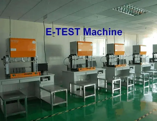
Ensuring quality and functionality of the finished PCB.
- Methods:
- Electrical conductivity tests
- Automated Optical Inspection (AOI)
- Hole plating verification
- Component fit checks
10. Panelization (If Required)
Arranging individual PCBs for efficient assembly.
- Process:
- Arrange PCB units in a panel frame
- Create score lines for easy separation after assembly
11. Assembly (Optional)
If requested, components can be mounted on the PCB.
- Methods:
- Manual soldering
- Automated surface-mount assembly
Key Differences from FR-4 PCB Manufacturing
While the overall process is similar, aluminum PCBs require some special considerations:
- Special surface treatments for the aluminum substrate
- High-temperature copper bonding process
- More relaxed design rules allowing thicker copper
- Special soldering techniques due to aluminum’s heat sensitivity
- Use of more flexible materials for drilling and routing
Applications of Aluminum PCBs
Aluminum PCBs excel in various high-performance applications:
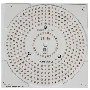
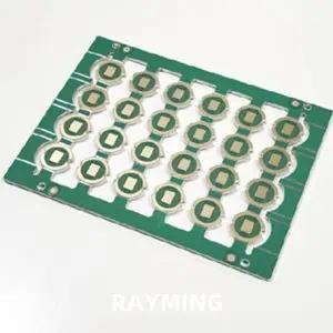
- High-power LED lighting
- Automotive electronics
- Power electronics and inverters
- Industrial motor drives
- RF and wireless infrastructure
- Aerospace and military systems
Conclusion: The Future of PCB Manufacturing
As electronics continue to demand higher power and better thermal management, aluminum PCBs are set to play an increasingly important role. Their unique properties make them ideal for a wide range of applications, from everyday consumer electronics to cutting-edge industrial and military systems.
By understanding the aluminum PCB manufacturing process, designers and engineers can better leverage these innovative boards to create more efficient, powerful, and reliable electronic systems. As technology advances, we can expect to see even more applications benefiting from the unique properties of aluminum PCBs.