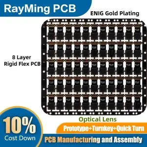
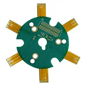
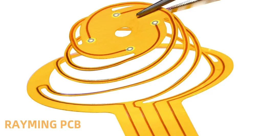
Flex Printed Circuit Boards (PCBs) provide unmatched design flexibility, enabling innovative solutions across industries like aerospace, medical devices, and consumer electronics. Renowned for their ability to bend and fold, flex PCBs deliver substantial space and weight savings, making them ideal for compact and lightweight applications.
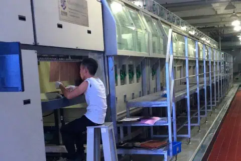
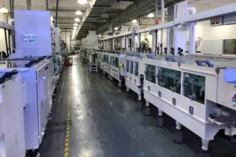
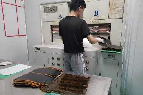
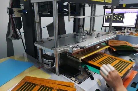
Below, explore our image gallery showcasing the flex PCB manufacturing process. From material preparation and etching to drilling, plating, and final fabrication, each step is meticulously executed to ensure precision and quality.
What is Flex PCB?
Let’s start with the basics. A Flex PCB, or Flexible Printed Circuit Board, is exactly what it sounds like – a circuit board that can bend! Unlike their rigid cousins, Flex PCBs are made with materials that allow them to twist and turn without breaking.
Why are Flex PCBs so cool? Here’s why:
- They’re bendy: You can fold them without damaging the circuits.
- They’re light: Much lighter than regular PCBs.
- They’re space-savers: Perfect for tight spots in gadgets.
- They’re tough: They can handle shakes and vibrations better.
- They’re good with heat: They can spread heat more effectively.
These features make Flex PCBs perfect for smartphones, smartwatches, and even cars!
Learn more about:
- PCB Manufacuring Process
- PCB Assembly Process
- Rigid Flex PCB Manufacturing Process
- Flex PCB Assembly
- Rigid Flex PCB Assembly
Flex PCB Manufacturing Process: 17 Steps to Flexibility
Now, let’s dive into how these flexible wonders are made. The process involves 17 crucial steps. Don’t worry; we’ll break it down for you!
1. Material Preparation (Pre-Clean)

First things first, we start with cleaning. The flexible material (usually polyimide or polyester) is thoroughly cleaned. It’s like giving the PCB a bath before its big day!
2. NC Drilling
Next up, we drill holes. But not just any holes – precise, computer-controlled holes. These will help connect different parts of the circuit later.
3. Copper Plating Process
Now, we give the board a copper coat. This step is crucial because copper is what makes the board conduct electricity.
4. Dry Film Lamination
Think of this step as putting a sticker on the board. We apply a special light-sensitive film that will help us create the circuit pattern.
5. LDI Exposure
Here’s where it gets cool. We use lasers to draw the circuit pattern on the film. It’s like a high-tech laser show, but for circuit boards!
6. Develop /Etch/ Stripping
This step is a bit like developing a photograph. We remove parts of the film and copper to reveal our circuit pattern.
7. AOI Testing
Time for a quality check! Cameras inspect the board to make sure everything looks good. It’s like giving the board an eye test.
8. Coverlay Layup
Now we add a protective layer called the coverlay. It’s like putting a jacket on the circuit to keep it safe.
9. Coverlay Lamination
We use heat and pressure to stick the coverlay to the board. It’s like ironing the jacket onto the circuit.
10. Hole Punching
We punch more holes for things like mounting the board or connecting components. Precision is key here!
11. Surface Finish (Immersion Gold)
We give the board a golden touch. This thin layer of gold protects the copper and makes it easier to solder components later.
12. Silkscreen Printing
Now we add labels and markings. It’s like giving the board its own set of instructions.
13. Electrical Test
Time to see if it works! We run electricity through the board to check if all connections are good.
14. Stiffener Application
Some parts of the board need to be rigid. We add stiffeners to these areas, like giving the board a backbone.
15. Outline Punching
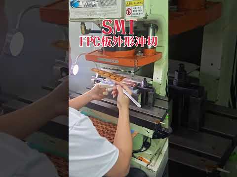
We cut the board to its final shape. It’s like giving the PCB its unique identity!
16. FQC (Final Quality Control)
One last check to make sure everything is perfect. We inspect the board from top to bottom.
17. Package and Shipping
Finally, we wrap it up and send it off. The Flex PCB is ready for its new home in a cool gadget!
Single Layer vs. Double Layer: A Tale of Two Flex PCBs

Flex PCBs come in two main flavors: single-layer and double-layer. Let’s see how they differ.
Single-sided Flexible PCB: The Simple Sibling
Single-sided Flex PCBs have circuits on just one side. Here’s a quick rundown of how they’re made:
- Cut the material
- Drill holes
- Add the circuit pattern
- Protect the circuit
- Add finishes and labels
- Test and ship
It’s simpler and cheaper, perfect for basic designs.
Double-sided Flexible PCB: The Complex Cousin
Double-sided Flex PCBs have circuits on both sides. Their manufacturing process is a bit more involved:
- Cut and drill
- Add circuits to both sides
- Connect the two sides
- Protect the circuits
- Add finishes and labels
- Test thoroughly
- Cut to shape and ship
This type allows for more complex designs but takes more time and money to make.
Wrapping It Up
And there you have it! From a simple flexible sheet to a high-tech, bendable circuit board, the journey of a Flex PCB is quite amazing. Whether it’s the simpler single-sided or the more complex double-sided version, these flexible marvels are changing the way we design electronics.
Next time you use your smartphone or put on a smartwatch, remember the incredible process behind the flexible circuits that make it all possible. The world of Flex PCBs is constantly evolving, paving the way for even cooler, more flexible gadgets in the future. Exciting times ahead in the world of electronics!