Introduction
Applying a solder mask to a Printed Circuit Board (PCB) is a crucial step in the PCB manufacturing process. The solder mask protects the copper traces from oxidation, prevents solder bridges, and enhances the overall durability of the board. While professional PCB manufacturers use advanced equipment to apply solder masks, it is possible to apply a UV solder mask at home with the right tools and techniques. This guide provides a comprehensive, step-by-step process for applying UV solder mask to your PCB board at home.
1. Understanding UV Solder Mask
1.1 What is UV Solder Mask?
UV solder mask is a type of solder resist that cures (hardens) when exposed to ultraviolet (UV) light. It is typically supplied as a liquid or film and is applied to the PCB to cover the copper traces, leaving only the pads exposed for soldering.
1.2 Benefits of UV Solder Mask
- Protection: Protects copper traces from oxidation and environmental damage.
- Insulation: Prevents electrical shorts by insulating conductive traces.
- Solder Control: Prevents solder from bridging between closely spaced pads.
- Aesthetic Appeal: Provides a professional finish to the PCB.
1.3 Tools and Materials Required
To apply UV solder mask at home, you will need the following tools and materials:
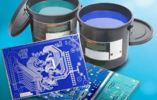
- UV Solder Mask Liquid or Film: Available in various colors (green, blue, red, etc.).
- UV Light Source: A UV lamp or UV curing chamber.
- Squeegee or Brush: For spreading the solder mask evenly.
- Photo Film or Transparency Sheet: For creating a solder mask stencil.
- PCB Cleaning Supplies: Isopropyl alcohol, lint-free cloth, and a brush.
- Plastic Container: For mixing and storing the solder mask.
- Protective Gear: Gloves, safety glasses, and a mask to protect against fumes.
2. Step-by-Step Guide to Applying UV Solder Mask
2.1 Step 1: Prepare the PCB
2.1.1 Clean the PCB
Before applying the solder mask, ensure that the PCB is clean and free of dust, grease, and oxidation. Follow these steps:
- Wipe the PCB with a lint-free cloth soaked in isopropyl alcohol.
- Use a soft brush to remove any debris from the traces and pads.
- Allow the PCB to dry completely.
2.1.2 Inspect the PCB
Inspect the PCB for any defects, such as scratches or exposed copper. Repair any issues before proceeding.
2.2 Step 2: Create the Solder Mask Stencil
2.2.1 Design the Stencil
Using PCB design software (e.g., KiCad, Eagle, or Altium), create a solder mask layer that exposes only the pads and vias. Export this layer as a high-resolution image or PDF.
2.2.2 Print the Stencil
Print the solder mask layer onto a photo film or transparency sheet using a laser printer. Ensure that the print is dark and opaque to block UV light effectively.
2.3 Step 3: Apply the UV Solder Mask
2.3.1 Mix the Solder Mask (if required)
If using a two-part UV solder mask, mix the components according to the manufacturer’s instructions. Stir gently to avoid introducing air bubbles.
2.3.2 Apply the Solder Mask
There are two main methods for applying UV solder mask: liquid application and film application.
Liquid Application Method:
- Pour a small amount of UV solder mask liquid onto the PCB.
- Use a squeegee or brush to spread the liquid evenly over the entire surface.
- Ensure that the solder mask covers all the traces while leaving the pads exposed.
Film Application Method:
- Cut a piece of UV solder mask film slightly larger than the PCB.
- Peel off the protective layer and carefully place the film onto the PCB.
- Use a roller or squeegee to remove air bubbles and ensure proper adhesion.
2.4 Step 4: Align and Expose the Stencil
2.4.1 Align the Stencil
Place the printed photo film or transparency sheet over the PCB, ensuring that the pads and vias align perfectly with the openings in the stencil.
2.4.2 Expose to UV Light
- Place the PCB and stencil under the UV light source.
- Expose the PCB to UV light for the recommended duration (usually 1-5 minutes, depending on the solder mask and UV light intensity).
- Rotate the PCB if necessary to ensure even exposure.
2.5 Step 5: Develop the Solder Mask
2.5.1 Remove the Stencil
After exposure, carefully remove the photo film or transparency sheet from the PCB.
2.5.2 Rinse the PCB
Rinse the PCB with water or a developer solution (as specified by the solder mask manufacturer) to remove the uncured solder mask. Use a soft brush to gently scrub the surface.
2.5.3 Dry the PCB
Allow the PCB to dry completely. You can use compressed air or a lint-free cloth to speed up the drying process.
2.6 Step 6: Cure the Solder Mask
2.6.1 Final UV Exposure
Place the PCB under the UV light source again for a final cure. This step ensures that the solder mask is fully hardened and durable.
2.6.2 Inspect the PCB
Inspect the PCB for any defects, such as incomplete coverage or misaligned pads. Touch up any areas if necessary.
3. Tips for Success
3.1 Work in a Clean Environment
Dust and debris can affect the quality of the solder mask application. Work in a clean, well-ventilated area to minimize contamination.
3.2 Use High-Quality Materials
Invest in high-quality UV solder mask and photo film to ensure the best results. Cheap materials may lead to poor adhesion or incomplete curing.
3.3 Practice on Scrap PCBs
If you are new to applying solder masks, practice on scrap PCBs before working on your final project. This will help you refine your technique and avoid mistakes.
3.4 Follow Manufacturer Instructions
Always follow the manufacturer’s instructions for mixing, applying, and curing the solder mask. Different products may have specific requirements.
4. Troubleshooting Common Issues
4.1 Incomplete Coverage
- Cause: Insufficient solder mask application or uneven spreading.
- Solution: Apply a thicker layer of solder mask and use a squeegee to spread it evenly.
4.2 Solder Mask Peeling
- Cause: Poor adhesion due to contamination or improper curing.
- Solution: Clean the PCB thoroughly before application and ensure proper UV exposure.
4.3 Misaligned Pads
- Cause: Incorrect alignment of the stencil.
- Solution: Double-check the alignment before exposing the PCB to UV light.
4.4 Air Bubbles
- Cause: Trapped air during application.
- Solution: Use a roller or squeegee to remove air bubbles before curing.
5. Advantages of Applying UV Solder Mask at Home
5.1 Cost-Effective
Applying solder mask at home can save money compared to outsourcing the process to a professional PCB manufacturer.
5.2 Customization
You have full control over the design and application process, allowing for greater customization.
5.3 Learning Experience
The process provides valuable hands-on experience and a deeper understanding of PCB manufacturing.
Conclusion
Applying UV solder mask to your PCB board at home is a rewarding and cost-effective way to enhance the durability and functionality of your PCBs. By following the step-by-step guide outlined above, you can achieve professional-quality results with the right tools and techniques. Whether you are a hobbyist or a professional, mastering this skill will enable you to create high-quality PCBs for a wide range of applications. With practice and attention to detail, you can confidently apply UV solder mask to your PCB projects at home.