
RAYPCB · ENGINEERING REFERENCE
Conductive vs Non-Conductive Via Fill: Engineering Guide
Separate electrical conductivity, thermal conductivity and solderable surface requirements. Compare two documented fill candidates in an explicit thermal model.
Original engineering guidance · References checked September 27, 2026
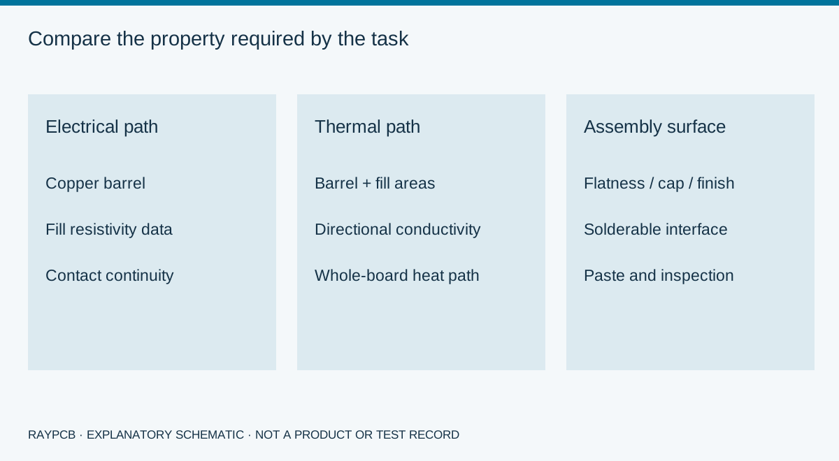
Conductive versus non-conductive via fill is a property decision
The useful comparison is not which name sounds better. It is which completed via construction supplies the required electrical path, thermal path and assembly surface. A non-conductive filler can occupy a hole whose plated copper barrel remains conductive. A conductive paste may add a path, but its properties are not automatically those of solid copper. Electroplated copper fill is a distinct process route.
Start by naming the function that the filler must perform. If the task is a flat solderable land, define the fill, cap and finish together. If the task is heat transfer, compare geometry and documented thermal properties within a stated model. If the task is electrical conduction through the filler itself, request resistivity and contact information separately. These decisions should not be collapsed into one “conductive” checkbox.
Keep three different questions on the comparison sheet
| Question | Non-conductive filler | Conductive paste or other conductive fill | Evidence needed |
|---|---|---|---|
| Where does electrical current flow? | The plated barrel can remain the intended path | Additional behavior depends on actual material and contacts | Completed geometry, resistivity and connection requirements |
| How does heat cross the board? | Barrel and filler contribute according to area and conductivity | A different filler may change the axial path | Directional thermal data and the complete heat path |
| What surface receives solder? | May use a separately specified metal cap and finish | Conductivity alone does not establish solderability | Surface construction and assembly review |
| Is processing compatible? | Cure and adhesion require review | Particle system, cure and surface treatment require review | Approved process sequence and material documentation |
| What does it cost? | Depends on selected route and verification | Depends on selected route and verification | Matched supplier quotation scope |
A conductive designation can refer to electrical behavior, thermal behavior or both. Read the units. Electrical resistivity and thermal conductivity are different measured properties, and the test conditions matter. A thermally improved polymer should not be assumed electrically conductive without the relevant data. Likewise, a conductive surface does not establish the material's behavior through its thickness.
Compare two candidates in an ideal axial thermal path
The worksheet treats each via as a uniform copper cylinder wall surrounding a filled circular lumen. Copper and filler conduct heat in parallel along the same length. The model then places an entered number of identical vias in ideal parallel. Use it to understand sensitivity to geometry and conductivity, not to predict the finished product's junction temperature.
RAYPCB ENGINEERING
HDI GeometryVia-Fill Thermal Path Comparison
Loading Via-Fill Thermal Path Comparison…
The diameter field means the open lumen inside the plated barrel before filling. The copper-thickness field is radial wall thickness; the outside diameter is therefore the lumen diameter plus twice that thickness. Confusing drill diameter with finished lumen or adding the plating only once changes the calculated copper area. Record which dimensions your drawing or measurement actually supplies.
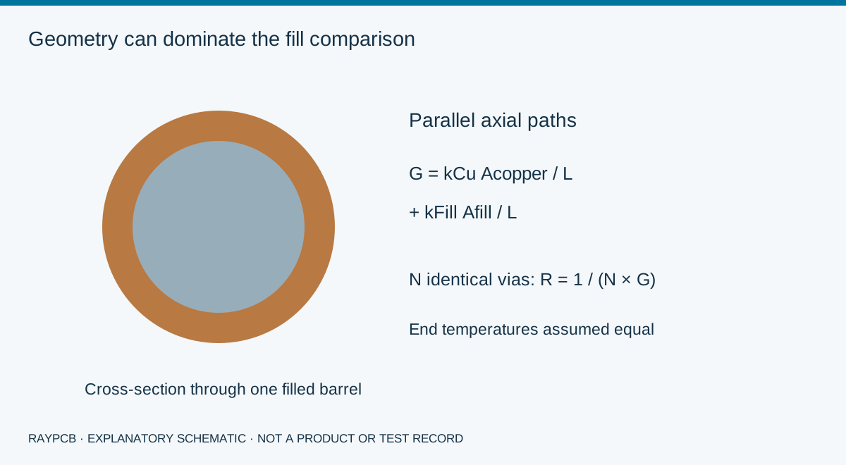
The model uses conductance G = kCu × Acopper / L + kFill × Afill / L. For N identical paths, resistance is 1 / (N × G). This follows ideal one-dimensional conduction through parallel areas. The Texas Instruments PCB thermal-conduction application report provides broader background on separating thermal paths. Its application context is temperature sensing; it does not validate a RAYPCB construction or the worksheet's illustrative property values.
Why a large filler-property change may give a small segment change
Consider the illustrative worksheet values: a 0.20 mm finished lumen, 25 µm radial copper wall, 1.60 mm segment length and ten identical vias. Copper conductivity is entered as 400 W/(m·K), while candidate fillers are entered as 0.5 and 5 W/(m·K). These are teaching values, not specifications for named products or measured production materials.
The copper shell already provides a substantial path in that example. Increasing only the fill conductivity changes one contribution to the combined conductance; it does not multiply the conductivity of the whole via by the same factor. The calculator reports both ideal segment resistances and a signed percentage change. If candidate B performs worse within the model, the result remains negative rather than being relabeled a saving.
Changing the via count, copper wall thickness or path length can change the comparison. Those changes may also affect layout, fabrication or assembly constraints, which the thermal equation does not evaluate. Do not optimize the numerical output in isolation from the construction. A larger or more numerous via arrangement must still fit the land, planes and manufacturing requirements.
The board is more than the via segment
The model assumes equal temperatures across each end of the parallel paths and perfect contact within the segment. It omits spreading in pads and planes, contact resistance, voids, package interfaces, heat-sink attachment and heat transfer to the surroundings. Actual heat must reach the via array and leave it. Either neighboring part of the path can dominate the installed thermal performance.
It also does not calculate current capacity. Thermal conductivity cannot be substituted for electrical resistivity, and a temperature-rise calculation needs a broader electrical and thermal model. If a proposed filler is intended to carry current, identify the conductor cross-section, contacts, permissible loss and operating conditions through a separate engineering review.
An array of ten vias does not always behave like ten perfectly equal parallel paths in the assembled product. Local heat spreading, placement and copper connections can make their contributions unequal. The simplified result is best used to decide which variables deserve a more complete analysis or measurement, then to document the assumptions carried into that next step.
Compare documents before comparing marketing descriptions
For each candidate, request the exact grade, cured or processed state, property direction, temperature, test method and revision. Record whether a value is typical data, a controlled specification or a supplier statement for a particular sample. Avoid combining a thermal value from one grade with a processing recommendation from another simply because both are described as via-fill materials.
Taiyo America's official hole-plugging and filling product catalogue provides an entry point to material-specific literature. Use the exact grade and current supplier document when comparing candidates. The link is not a claim that a listed material is stocked, approved or used by RAYPCB. No catalogue property is automatically inserted into this worksheet.
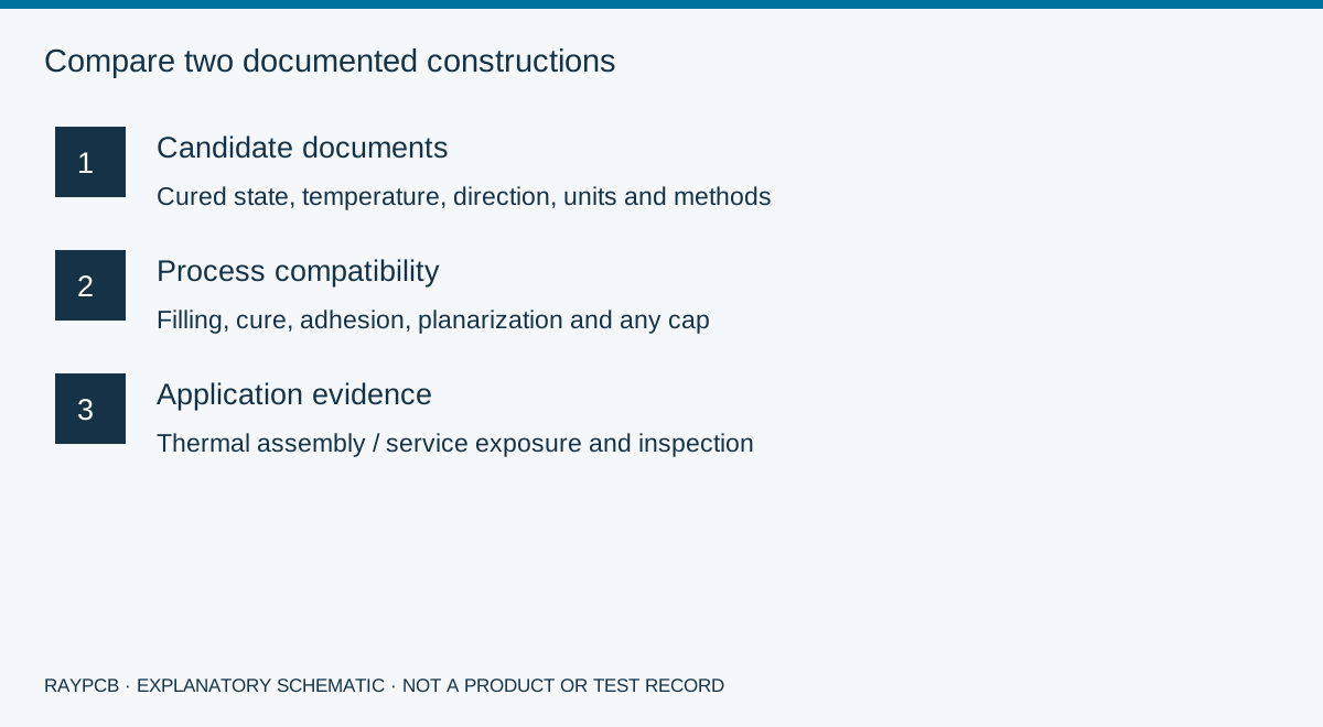
Electrical properties, thermal properties, adhesion and compatibility with subsequent processing should remain separate rows in the selection record. A material can be attractive on one axis while requiring additional work on another. Keep unknown values visible. An empty field is a reason to request evidence, not an invitation to substitute a convenient number from a different product.
The assembly surface may determine the practical route
For a via inside a component land, the package and assembly requirements can be more decisive than a modest improvement in ideal segment thermal resistance. Specify whether a metal cap and final finish are needed and how the finished surface will be assessed. A conductive filler should not be assumed to supply the required solderable interface on its own.
The BGA via-in-pad review focuses on that land interface. The PCB via-filling process page defines the manufacturing route and provides a process-specific budget worksheet. Keep the decision sequence clear: first agree what the completed feature must do, then compare routes and quotations that deliver that same feature.
Compare complete routes with the same scope
Cost depends on more than the price of a filler. Selected hole populations, preparation, filling, cure or plating, planarization, any cap, panel handling and verification can all be part of the route. A material comparison that omits downstream operations may create a misleading cost conclusion.
Ask each quotation to identify the finished structure, applicable sides, selected population and evidence included. If one offer includes a cap and inspection while another covers only a filling step, normalize the scope before comparing totals. Do not apply a generic percentage premium to every conductive fill; no verified supplier pricing model supports that shortcut here.
Changing material also creates a revision-control task. Record whether the alternative is an approved equivalent or a proposal requiring validation. A procurement substitution should not silently alter the drawing's electrical, thermal or assembly assumptions. For a complete construction discussion, use HDI PCB manufacturing or send the requirement directly through Contact.
Questions that clarify the comparison
Does non-conductive fill make a plated via electrically open?
Not by its name alone. The plated copper barrel can remain the intended electrical connection. Review the actual barrel, lands and interfaces. If electrical conduction through the filler itself is required, that is a separate material and contact requirement.
Is conductive paste equivalent to electroplated copper fill?
No. They are different material and process routes. Properties, interfaces, processing and final surface need to be specified for the proposed construction. Do not assign bulk-copper properties to a paste without appropriate evidence.
Can this tool tell me the board temperature?
No. It compares an ideal via segment under explicit assumptions. It excludes the surrounding board, package, heat sink and environment. Use the result to inform a complete thermal model or measurement plan, not as a junction-temperature prediction.
Which fill should I choose for a thermal pad?
Start with the package guidance and the complete heat-transfer and assembly requirements. Compare documented constructions rather than selecting from a label. The best next step may be a layout or copper-path change, a different fill route, or additional evidence about the existing design.
Bring the requirement and the drawing together
Send the board revision, construction, quantity and the standard or engineering question you need reviewed. Identify unresolved requirements so the response can address them.
Send requirements for reviewOptional: attach the downloaded worksheet manually. This guidance does not certify a design, approve a shipment or replace the applicable authorized standards.