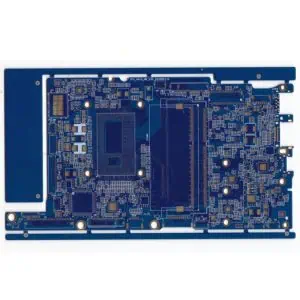
Designing and Manufacturing 3-Layer ENIG Rigid-Flex PCBs
Rigid-Flex PCBs combine the best features of rigid and flexible circuits, offering a unique solution for complex electronic designs. This guide will walk you through the process of designing and manufacturing a 3-layer ENIG Rigid-Flex PCB.
Understanding Rigid-Flex PCBs
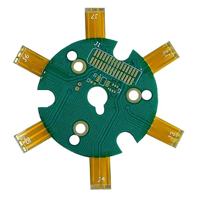
Rigid-Flex PCBs consist of rigid and flexible sections in a single board. The flexible parts allow the PCB to bend and fold, while the rigid sections provide stability for components. A 3-layer design typically includes:
- Top layer (rigid)
- Middle layer (flexible)
- Bottom layer (rigid)
The ENIG (Electroless Nickel Immersion Gold) finish provides excellent solderability and protection against oxidation.
Design Considerations
1. Layer Stack-up
- Top Layer: Rigid FR-4 material
- Middle Layer: Flexible polyimide
- Bottom Layer: Rigid FR-4 material
Ensure proper adhesion between layers using specialized adhesives.
2. Trace Routing
- Use wider traces on flex areas to improve durability
- Avoid 90-degree angles in flex regions; use curved traces instead
- Place traces perpendicular to the bend axis in flex areas
3. Component Placement
- Keep components on rigid sections whenever possible
- If components must be on flex areas, use smaller, lighter components
- Avoid placing components near transition zones between rigid and flex sections
4. Mechanical Design
- Define bend radii and folding requirements early in the design process
- Use stiffeners or support structures in areas prone to stress
- Consider strain relief features at the rigid-flex interfaces
5. Material Selection
- Choose appropriate flex materials (e.g., polyimide) for the middle layer
- Select rigid materials (e.g., FR-4) compatible with flex materials
- Ensure all materials can withstand the ENIG plating process
Manufacturing Process
1. Preparation
- Create separate design files for rigid and flex sections
- Provide detailed stack-up information to the manufacturer
- Specify areas requiring special attention (e.g., bend zones)
2. Fabrication
a. Rigid Section Fabrication:
- Drill holes and vias in rigid sections
- Pattern and etch copper layers
- Apply solder mask and silkscreen
b. Flexible Section Fabrication:
- Pattern and etch flexible copper layer
- Apply coverlay (protective layer) to the flex section
c. Lamination:
- Bond rigid and flex sections using specialized adhesives
- Apply heat and pressure to ensure proper adhesion
3. ENIG Plating Process
- Clean and prepare the surface
- Apply catalytic coating
- Deposit electroless nickel layer (typically 3-6 μm thick)
- Immerse in gold solution for final gold layer (typically 0.05-0.1 μm thick)
4. Cutting and Shaping
- Use precision cutting tools (e.g., laser or die-cutting) to define board outline
- Pay special attention to flex areas to avoid damage
5. Testing and Quality Control
- Perform electrical continuity tests
- Check for proper adhesion between layers
- Conduct bend and flex tests to ensure durability
- Inspect ENIG finish for uniformity and quality
Design Rules and Best Practices
- Maintain a minimum bend radius of 10 times the flex circuit thickness
- Use hatched polygons instead of solid copper pours in flex areas
- Implement teardrop patterns at pad-to-trace connections for improved reliability
- Avoid placing vias in flex areas; if necessary, use “via-in-pad” design
- Consider using selective stiffeners in areas requiring additional support
Challenges and Solutions
- Layer Registration: Use fiducial markers for accurate alignment during manufacturing
- Flexibility vs. Durability: Balance the number of layers and material thickness
- Cost Management: Optimize design to minimize waste and reduce manufacturing complexity
- Signal Integrity: Use proper grounding techniques and consider impedance control in critical areas
Conclusion
Designing and manufacturing 3-layer ENIG Rigid-Flex PCBs requires careful planning and attention to detail. By following these guidelines and working closely with your PCB manufacturer, you can create high-quality, reliable Rigid-Flex PCBs suitable for a wide range of applications, from consumer electronics to aerospace and medical devices.
Remember that each design is unique, and you may need to adjust these guidelines based on your specific requirements and constraints. Always consult with your PCB manufacturer early in the design process to ensure manufacturability and optimize your design for cost-effectiveness and performance.