Introduction
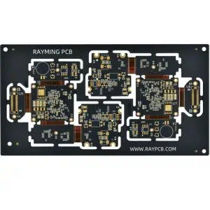
Flexible Printed Circuit boards (FPCs) have revolutionized electronic design, allowing for compact, lightweight, and bendable electronic circuits. A 0.2mm 6 layer FPC represents the cutting edge of this technology, offering high component density and flexibility in an ultra-thin package. This document outlines the process of designing and manufacturing these sophisticated circuits.
Design Considerations
Material Selection
The choice of materials is crucial for a 0.2mm 6 layer FPC:
-
Base Material: Polyimide is the most common choice due to its excellent thermal stability and flexibility. For a 0.2mm board, ultra-thin polyimide films (12.5-25µm) are used.
-
Copper Foil: Ultra-thin copper foils (5-9µm) are essential to achieve the target thickness while maintaining six layers.
-
Adhesive: Specialized thin adhesives (12.5-25µm) are used to bond layers without compromising flexibility or increasing thickness significantly.
Layer Stack-up
A typical layer stack-up for a 0.2mm 6 layer FPC might look like this:
- Top layer: 5µm copper
- Adhesive: 12.5µm
- Polyimide: 12.5µm
- Inner layer 1: 5µm copper
- Adhesive: 12.5µm
- Polyimide: 12.5µm
- Inner layer 2: 5µm copper
- Adhesive: 12.5µm
- Polyimide: 12.5µm
- Inner layer 3: 5µm copper
- Adhesive: 12.5µm
- Polyimide: 12.5µm
- Inner layer 4: 5µm copper
- Adhesive: 12.5µm
- Polyimide: 12.5µm
- Bottom layer: 5µm copper
Total thickness: approximately 0.2mm
Circuit Design
When designing the circuit:
- Trace Width and Spacing: Use ultra-fine traces (as small as 50µm) and spacing to maximize routing density.
- Via Technology: Utilize micro vias (50-100µm) and buried/stacked vias to connect layers while minimizing board thickness.
- Bend Radius: Design traces to run perpendicular to bend lines where possible. Avoid placing components in areas of high stress.
- Shielding: Consider incorporating shielding layers for EMI protection, especially important in dense, multi-layer designs.
Manufacturing Process
1. Preparation
- Create and verify Gerber files, ensuring all layers align correctly.
- Prepare materials: polyimide films, copper foils, and adhesives.
2. Inner Layer Processing
- Clean and prepare copper foils.
- Apply photoresist to copper layers.
- Expose and develop the circuit pattern.
- Etch copper to create traces.
- Strip remaining photoresist.
- Optically inspect layers for defects.
3. Lamination
- Stack layers with adhesive films between each layer.
- Use a precision lamination press with controlled temperature and pressure.
- Ensure proper alignment of all layers.
4. Drilling
- Use high-speed, precision drilling machines for through-holes and vias.
- Employ laser drilling for micro vias.
5. Plating
- Clean and activate holes.
- Electroless copper plate the holes.
- Electrolytic copper plate to build up copper thickness.
6. Outer Layer Imaging
- Apply, expose, and develop photoresist on outer layers.
- Etch copper to create final outer layer circuitry.
7. Solder Mask and Surface Finish
- Apply liquid photo-imageable solder mask.
- Expose, develop, and cure solder mask.
- Apply surface finish (e.g., ENIG, immersion tin) to exposed copper.
8. Profiling
- Use precision routing or laser cutting to achieve the final board shape.
- Take care to avoid delamination during cutting.
9. Testing
- Perform electrical continuity and isolation tests.
- Conduct bend testing to ensure flexibility and durability.
Challenges and Solutions
1. Layer Alignment
Challenge: Maintaining precise alignment of ultra-thin layers. Solution: Use advanced optical alignment systems and fiducial marks.
2. Thickness Control
Challenge: Achieving and maintaining the 0.2mm thickness across the board. Solution: Employ precision-controlled lamination processes and real-time thickness monitoring.
3. Flexibility vs. Durability
Challenge: Balancing the need for flexibility with mechanical strength. Solution: Optimize material selection and layer stack-up. Consider selective stiffeners in high-stress areas.
4. Fine Feature Resolution
Challenge: Achieving and maintaining fine traces and spaces. Solution: Use advanced imaging techniques like LDI (Laser Direct Imaging) for higher resolution.
5. Thermal Management
Challenge: Managing heat in a densely packed, thin board. Solution: Incorporate thermal vias and consider the use of thermally conductive adhesives.
Conclusion
Designing and manufacturing a 0.2mm 6 layer Flexible Printed Circuit board requires a combination of cutting-edge materials, precise design techniques, and advanced manufacturing processes. While challenging, these ultra-thin, multi-layer FPCs enable the creation of incredibly compact and flexible electronic devices, pushing the boundaries of what’s possible in fields like wearable technology, medical devices, and aerospace applications.
As technology continues to advance, we can expect further innovations in materials and processes, potentially leading to even thinner and more capable flexible circuits in the future.


