In today’s electronics landscape, the relentless push for faster data transfer and processing speeds has transformed how engineers approach printed circuit board (PCB) design. High-speed PCBs have become the backbone of modern electronics, enabling everything from lightning-fast internet connections to advanced driver assistance systems in vehicles. Yet, as frequencies climb and signal rise times shrink to picoseconds, the very materials used to construct these boards have become critically important.
This article explores why low dielectric constant (Dk) and low dissipation factor (Df) materials are not merely beneficial but essential for high-speed PCB performance. Whether you’re designing next-generation telecommunications equipment or wrestling with signal integrity issues in your current project, understanding these material properties could be the difference between a mediocre and exceptional product.
What Is a High-Speed PCB?

Before diving into material considerations, let’s clarify what constitutes a “high-speed PCB.” Unlike conventional circuit boards, high-speed PCBs are specifically designed to maintain signal integrity at elevated frequencies and data rates.
Defining High-Speed in Modern Electronics
High-speed PCBs typically involve one or more of these characteristics:
- Signal rise times below 1 nanosecond
- Operating frequencies above 1 GHz
- Data rates exceeding 1 Gbps
- Transmission line effects becoming significant
It’s worth noting that “high-speed” is a relative term that continues to evolve. What was considered blazingly fast a decade ago might be regarded as moderate speed today. The threshold keeps advancing as technology progresses.
Real-World Applications
High-speed PCBs are ubiquitous in modern electronic systems:
- Network infrastructure (routers, switches, servers)
- High-performance computing platforms
- 5G telecommunications equipment
- Automotive radar and ADAS systems
- High-definition video processing
- Memory interfaces (DDR4/5, GDDR6)
- High-speed storage systems (NVMe, PCIe 4.0/5.0)
Signal Speed vs. Clock Speed
One common misconception is equating a PCB’s “speed” with its clock frequency. While clock frequency is important, signal integrity depends more on signal rise time—how quickly a signal transitions from low to high. Faster rise times mean higher frequency components in the signal, requiring more careful attention to the board’s material properties.
As rise times decrease below 1 nanosecond, transmission line effects become pronounced, and the PCB substrate material significantly impacts signal propagation. This is where dielectric properties become crucial.
Read more about:
Understanding Dielectric Constant (Dk) and Dissipation Factor (Df)
The performance of high-speed PCBs hinges on two key material properties: dielectric constant (Dk) and dissipation factor (Df). Let’s break down what these properties mean and why they matter.
What is Dielectric Constant (Dk)?
The dielectric constant, often denoted as Dk, εr, or simply “Er,” measures how much a material concentrates electric flux compared to a vacuum. In simpler terms, it indicates how much a material slows down electrical signals passing through it.
A vacuum has a Dk of exactly 1.0, while PCB substrate materials typically range from 2.2 to 4.5. Lower Dk values mean signals travel faster through the material, which is generally desirable for high-speed applications.
The dielectric constant directly affects:
- Signal propagation velocity
- Impedance characteristics
- Electrical wavelength in the material
What is Dissipation Factor (Df)?
The dissipation factor (Df), also known as the loss tangent or tan δ, measures how much signal energy is lost as heat within the dielectric material. It represents the inefficiency of the dielectric material.
A lower Df value indicates less signal loss, which means:
- Reduced signal attenuation
- Better signal integrity over distance
- Less power lost as heat
- Improved high-frequency performance
Typical Dk/Df Ranges for PCB Materials
PCB substrates exhibit a wide range of dielectric properties:
| Material Type | Typical Dk Range | Typical Df Range |
| Standard FR-4 | 4.0-4.7 | 0.017-0.025 |
| Mid-performance | 3.5-4.0 | 0.008-0.015 |
| High-performance | 2.8-3.5 | 0.002-0.007 |
| Ultra-low loss | 2.2-2.8 | 0.0009-0.002 |
Each material category serves different application needs, with higher performance materials generally commanding higher prices.
Why Low-Dk/Df Materials Are Essential for High-Speed PCBs
As frequencies climb above 1 GHz and data rates exceed multi-gigabit speeds, the material composition of PCBs becomes increasingly critical. Let’s explore why low-Dk/Df materials are not just beneficial but essential for high-speed PCB performance.
Signal Integrity Benefits
Minimizing Signal Delay
Lower Dk materials allow signals to propagate faster through the PCB. This becomes crucial in high-speed designs where timing margins are tight, and signal delays must be carefully managed.
The propagation delay (tpd) in a PCB trace is directly proportional to the square root of the dielectric constant:
tpd ∝ √Dk
For time-critical applications like DDR memory interfaces, where timing skew must be minimized, low-Dk materials provide essential performance advantages.
Reducing Signal Reflections
When signals encounter impedance discontinuities, reflections occur. These reflections can cause signal integrity issues like ringing and overshoot. Low-Dk materials enable more precise impedance control, reducing the likelihood of impedance mismatches and associated reflections.
Minimizing Signal Loss
Insertion Loss Reduction
Signal attenuation becomes a major concern at high frequencies. The dissipation factor (Df) directly contributes to insertion loss, which increases with frequency. Lower Df materials significantly reduce this loss, allowing signals to maintain integrity over longer distances.
The relationship between insertion loss and Df is approximately:
Insertion Loss (dB) ∝ Frequency × Df
This means that as frequencies increase, the benefits of low-Df materials become exponentially more important.
Maintaining Signal Shape
High-frequency signals are particularly vulnerable to dispersion—different frequency components traveling at different speeds. This can distort the signal shape, causing issues like intersymbol interference in digital systems. Low-Dk/Df materials help maintain signal fidelity by reducing dispersion effects.
Improved Design Flexibility
Enhanced Routing Capabilities
Low-Dk/Df materials allow for:
- Longer trace lengths before signal degradation becomes problematic
- Tighter routing constraints while maintaining signal integrity
- Reduced need for signal conditioning components
- More reliable performance across manufacturing variations
Frequency Consistency
Premium low-Dk/Df materials typically exhibit more stable dielectric properties across frequency ranges. This consistency is valuable for broadband applications where performance must be maintained across multiple frequency bands.
Comparing Common PCB Materials for High-Speed Applications
The PCB industry offers a spectrum of materials with varying performance characteristics. Let’s compare the most common options for high-speed applications.
FR-4 vs. High-Performance Laminates
Standard FR-4
For decades, FR-4 has been the workhorse of the PCB industry. This glass-reinforced epoxy laminate offers:
- Dk: 4.0-4.7
- Df: 0.017-0.025
- Good mechanical stability
- Excellent cost-effectiveness
- Widespread manufacturing support
However, standard FR-4 becomes problematic above 1-2 GHz due to its relatively high Df and Dk variation with frequency.
High-Performance FR-4
Modified FR-4 materials with enhanced dielectric properties bridge the gap between standard FR-4 and premium laminates:
- Dk: 3.5-4.0
- Df: 0.008-0.015
- Moderate cost increase
- Suitable for applications up to 5-10 GHz
Premium High-Speed Laminates
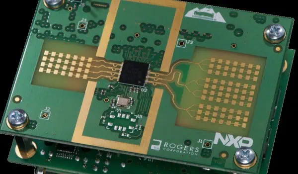
For the most demanding applications, manufacturers like Rogers, Isola, Panasonic (Megtron), and Taconic produce specialized materials:
Rogers Materials (e.g., RO4350B, RO3003)
- Dk: 2.8-3.5 (varies by grade)
- Df: 0.0025-0.004
- Excellent high-frequency performance
- Superior thermal stability
- Significantly higher cost than FR-4
Isola Materials (e.g., I-Speed, Tachyon)
- Dk: 3.0-3.5
- Df: 0.002-0.008
- Good balance of performance and processability
- Compatible with standard FR-4 manufacturing processes
Panasonic Megtron
- Dk: 3.3-3.7
- Df: 0.002-0.007
- Popular for server and high-speed computing applications
- Good thermal reliability
Material Performance at GHz Frequencies
At frequencies above 10 GHz, the differences between material types become dramatically apparent. Tests consistently show that:
- Standard FR-4 exhibits significant signal degradation beyond 5-10 GHz
- High-performance laminates maintain signal integrity up to 25+ GHz
- Ultra-low loss materials can support applications exceeding 50 GHz
Cost vs. Performance Trade-offs
The price differential between standard FR-4 and premium high-speed materials can be substantial:
- Standard FR-4: Base cost reference (1×)
- High-performance FR-4: 1.5-2× higher cost
- Premium laminates: 3-10× higher cost
Design engineers must balance material costs against performance requirements. Often, a hybrid approach works best—using premium materials only in critical areas while employing standard materials elsewhere.
Material Selection Considerations for High-Speed PCBs

Choosing the right material for your high-speed PCB requires balancing multiple factors. Here’s a systematic approach to material selection.
Application-Specific Requirements
Start by analyzing your specific requirements:
Frequency Range Considerations
- Up to 2 GHz: Enhanced FR-4 may be sufficient
- 2-10 GHz: High-performance FR-4 or entry-level specialty materials
- 10+ GHz: Premium low-loss materials are typically necessary
Signal Path Length
Longer signal paths suffer more from dielectric losses, making low-Df materials more important:
- Short traces (<6 inches): Material selection less critical
- Medium traces (6-12 inches): Consider enhanced materials
- Long traces (>12 inches): Premium low-loss materials may be essential
Layer Count Impact
Higher layer counts introduce additional challenges:
- Thinner dielectric layers between planes
- Greater risk of crosstalk
- More complex impedance control
Thermal and Mechanical Stability
High-speed applications often involve substantial power dissipation. Consider:
- Coefficient of thermal expansion (CTE) compatibility with components
- Glass transition temperature (Tg) suitable for operating conditions
- Thermal conductivity for heat dissipation
- Dimensional stability during manufacturing processes
Stackup Planning with Low-Dk Materials
Effective stackup design becomes particularly important with low-Dk materials:
- Impedance Control: Lower Dk values require wider traces for a given impedance
- Mixed-Material Stackups: Consider hybrid approaches using premium materials only where needed
- Prepreg Selection: Manage resin content for consistent dielectric properties
- Reference Plane Proximity: Optimize signal-to-ground spacing for controlled impedance
Industry Use Cases & Trends
High-speed PCB materials are evolving rapidly to meet the demands of cutting-edge applications. Let’s explore some key industry sectors driving this evolution.
5G Infrastructure
The rollout of 5G networks has pushed frequency requirements into millimeter-wave territory (24-40+ GHz), demanding:
- Ultra-low loss materials (Df < 0.002)
- Extremely stable Dk across temperature ranges
- Materials optimized for millimeter-wave antenna structures
- Reduced signal loss for massive MIMO implementations
Material innovations specifically targeting 5G include modified PTFE composites and ceramic-filled hydrocarbon resins with exceptional high-frequency performance.
Automotive Radar and Sensors
Advanced driver assistance systems (ADAS) and autonomous driving technologies rely on high-frequency radar (typically 77-81 GHz) and other sensors requiring:
- Materials with low moisture absorption
- Temperature stability from -40°C to +125°C
- Consistent performance in harsh environmental conditions
- Reliability for safety-critical applications
Data Centers and Cloud Hardware
The exponential growth in data center traffic has driven adoption of:
- 56G and 112G SerDes channels
- PAM4 signaling requiring exceptional signal integrity
- Materials optimized for backplane and midplane applications
- Solutions balancing performance with thermal management
Emerging Trends in High-Speed Material Technology
The high-speed PCB materials market continues to innovate:
- Spread-glass technologies: Reducing the “fiber weave effect” that causes Dk variation
- Ultra-smooth copper foils: Minimizing conductor losses at high frequencies
- Halogen-free formulations: Meeting environmental regulations while maintaining performance
- Thermally conductive dielectrics: Addressing heat dissipation challenges
- Advanced material characterization: More accurate modeling of material behavior up to millimeter-wave frequencies
Conclusion
The demanding requirements of high-speed PCB applications have fundamentally changed how we approach material selection. Low-Dk/Df materials are no longer luxury options but essential components for designs operating at multi-gigabit data rates or gigahertz frequencies.
As signals continue to accelerate, the performance gap between standard and premium materials widens. Engineers must carefully balance the higher material costs against the performance benefits, considering the entire system context rather than focusing solely on material specifications.
The future of high-speed PCB materials looks promising, with continued innovation driving both performance improvements and cost reductions. Emerging technologies like silicon photonics and chiplet architectures will create new challenges and opportunities for material scientists and PCB designers alike.
Ultimately, success in high-speed PCB design requires a holistic approach—understanding not just the materials themselves but how they interact with other design elements to create a cohesive, high-performing system.
FAQ Section
What is a good Dk value for high-speed PCBs?
For high-speed applications, materials with Dk values between 3.0 and 3.8 provide a good balance of performance and cost. Ultra-high-speed designs (above 25 GHz) benefit from even lower Dk values (2.2-2.8), though these materials typically come at a premium price.
Is FR-4 suitable for high-speed applications?
Standard FR-4 is generally suitable for frequencies up to 1-2 GHz. Enhanced FR-4 materials can perform adequately up to 5-10 GHz, depending on the specific formulation and application requirements. Beyond these frequencies, specialized high-speed laminates typically offer superior performance.
What happens if I use high-Df materials in high-speed designs?
Using materials with high dissipation factors (Df) in high-speed designs leads to increased signal attenuation, particularly at higher frequencies. This results in reduced signal amplitude, increased jitter, and potentially higher bit error rates. The impact becomes more severe as either frequency or trace length increases.
How do I balance cost and performance in high-speed material selection?
Consider a selective approach—using premium materials only in critical areas while employing standard materials elsewhere. For example, use high-performance laminates for critical signal layers and standard FR-4 for power and ground layers. Also, evaluate the total system cost, including potential savings from reduced signal conditioning components and fewer design iterations.
How much can material selection impact signal integrity?
Material selection can dramatically impact signal integrity. In high-speed designs, switching from standard FR-4 to a premium low-loss material can reduce insertion loss by 3-6 dB or more at 10 GHz over a 10-inch trace—potentially making the difference between a functioning and non-functioning design.