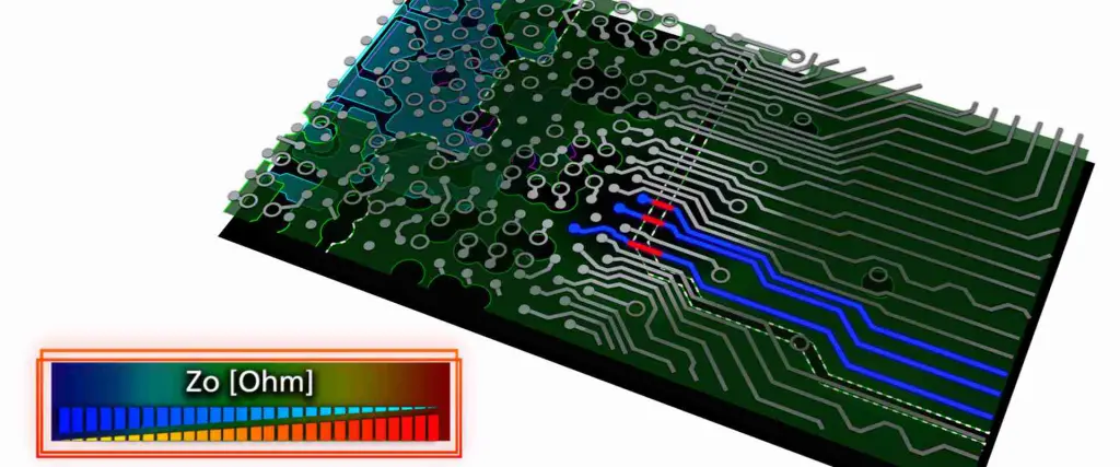
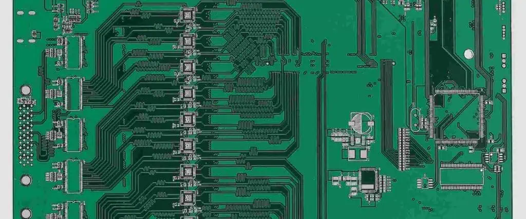
In the realm of high-speed printed circuit board (PCB) design, image planes play a crucial role in ensuring signal integrity, power distribution, and electromagnetic compatibility. This article delves into the intricacies of designing effective image planes for high-speed PCBs, covering key concepts, best practices, and advanced techniques to optimize performance.
Understanding Image Planes
What Are Image Planes?
Image planes, also known as reference planes or return planes, are large areas of copper on a PCB that serve as a return path for high-frequency signals and provide a low-impedance power distribution network.
Types of Image Planes
- Ground planes
- Power planes
- Split planes
Importance in High-Speed Design
Image planes are essential for:
- Maintaining signal integrity
- Reducing electromagnetic interference (EMI)
- Providing low-impedance power distribution
- Controlling impedance of transmission lines
Fundamentals of Image Plane Design

Plane Thickness and Material
The thickness and material of image planes affect their effectiveness in high-speed designs.
| Factor | Consideration |
| Copper Weight | 1 oz (35 µm) to 2 oz (70 µm) typical |
| Dielectric Material | FR-4, high-speed laminates (e.g., Rogers, Megtron) |
| Skin Depth | Influences high-frequency current flow |
Plane Spacing and Stackup Considerations
Proper spacing between planes and strategic placement within the PCB stackup are crucial for optimal performance.
Recommended Stackup Configurations
| Layer Count | Typical Stackup |
| 4-layer | Signal – Ground – Power – Signal |
| 6-layer | Signal – Ground – Signal – Power – Ground – Signal |
| 8-layer | Signal – Ground – Signal – Power – Ground – Power – Ground – Signal |
Plane Stitching and Via Placement
Effective stitching between planes ensures low-impedance return paths and reduces EMI.
Stitching Guidelines
- Use multiple vias for connections between planes
- Place stitching vias near high-speed signal vias
- Maintain a maximum distance of λ/20 between stitching vias (where λ is the wavelength of the highest frequency)
Advanced Image Plane Design Techniques
Partitioning and Zoning
Dividing image planes into separate areas for different power domains or functional blocks can improve isolation and reduce noise coupling.
Zoning Strategies
- Analog/Digital separation
- Noisy/Quiet circuit isolation
- Multiple voltage domain management
Plane Cutouts and Antipads
Strategic use of plane cutouts and antipads can control return current paths and reduce crosstalk.
Design Rules for Cutouts and Antipads
- Minimize cutout size to reduce impedance discontinuities
- Use antipads around vias to prevent unwanted coupling
- Maintain a 5H rule for plane edges (where H is the dielectric thickness)
Handling Plane Transitions
Proper handling of plane transitions is crucial for maintaining signal integrity in multi-layer designs.
Transition Techniques
- Via stitching at layer transitions
- Maintaining reference plane continuity
- Using ground vias for signal layer changes
Impedance Control and Image Planes

Calculating Trace Impedance
Image planes play a significant role in determining the impedance of transmission lines.
Impedance Calculation Factors
| Factor | Impact on Impedance |
| Trace Width | Wider traces lower impedance |
| Dielectric Thickness | Thicker dielectric increases impedance |
| Dielectric Constant | Higher εr lowers impedance |
| Plane Spacing | Greater spacing increases impedance |
Differential Pair Considerations
Designing image planes for differential pairs requires special attention to maintain consistent differential impedance.
Differential Pair Design Guidelines
- Route differential pairs over continuous ground planes
- Avoid splits or gaps in reference planes under differential pairs
- Maintain symmetry in the return path for both signals
Power Integrity and Image Planes
Plane Capacitance and Decoupling
Image planes contribute to the overall capacitance of the power distribution network (PDN).
Plane Pair Capacitance
The capacitance between power and ground planes can be estimated using:
C = (ε0 * εr * A) / d
Where:
- C is the capacitance
- ε0 is the permittivity of free space
- εr is the relative permittivity of the dielectric
- A is the area of the plane
- d is the distance between planes
Power Plane Segmentation
Segmenting power planes can help isolate noise and improve power integrity.
Segmentation Strategies
- Use separate plane areas for different voltage domains
- Implement guard traces or moats between plane segments
- Use ferrite beads or inductors for additional isolation
EMI Reduction Techniques
Edge Termination
Proper termination of plane edges can significantly reduce EMI radiation.
Edge Termination Methods
- Via stitching along plane edges
- Implementing ground rings
- Using edge plating on board perimeter
Slot Resonance Mitigation
Slots in image planes can create resonant structures that radiate EMI.
Slot Resonance Prevention
- Avoid long, narrow slots in planes
- Use multiple smaller slots instead of single large slots
- Implement stitching vias along slot edges
Signal Routing Considerations
Return Path Discontinuities
Minimizing return path discontinuities is crucial for maintaining signal integrity.
Best Practices
- Route high-speed signals over continuous reference planes
- Use stitching vias when crossing plane splits
- Avoid routing sensitive signals near plane edges or slots
Via Design and Placement
Proper via design and placement are essential for maintaining signal integrity and controlling EMI.
Via Design Guidelines

- Use ground vias adjacent to signal vias for improved return path
- Implement back-drilling for high-frequency signals
- Consider via stub effects in impedance calculations
Simulation and Analysis
Electromagnetic Field Solvers
Using electromagnetic field solvers can help validate image plane designs and identify potential issues.
Simulation Objectives
- Verify plane resonances
- Analyze current distribution
- Identify potential EMI hotspots
Time Domain Reflectometry (TDR)
TDR analysis can help identify impedance discontinuities and validate plane transitions.
TDR Applications
- Verifying trace impedance
- Identifying plane split effects
- Validating via transitions
Manufacturing Considerations
Plane Copper Pour Techniques
Proper copper pour techniques ensure uniform plane coverage and reduce impedance variations.
Copper Pour Guidelines
- Use thermal relief connections for component pads
- Implement hatched planes for improved flexibility in flex PCBs
- Maintain minimum copper width to ensure manufacturability
Controlled Impedance Fabrication
Working with PCB manufacturers to ensure controlled impedance fabrication is crucial for high-speed designs.
Fabrication Considerations
- Specify target impedances and tolerances
- Provide stackup details and dielectric requirements
- Request test coupons for impedance verification
Frequently Asked Questions
Q1: Why are image planes important in high-speed PCB design?
A1: Image planes are crucial in high-speed PCB design because they provide low-impedance return paths for signals, help maintain signal integrity, reduce electromagnetic interference (EMI), and enable controlled impedance transmission lines. They also play a vital role in power distribution and thermal management.
Q2: How do I choose the right stackup for my high-speed PCB?
A2: Choosing the right stackup depends on various factors, including the number of layers, signal integrity requirements, and power distribution needs. Generally, it’s recommended to have ground and power planes adjacent to signal layers. For example, a 4-layer board might use a Signal-Ground-Power-Signal configuration, while a 6-layer board could use Signal-Ground-Signal-Power-Ground-Signal.
Q3: What are the best practices for handling plane splits in high-speed designs?
A3: When dealing with plane splits in high-speed designs, consider the following best practices:
- Avoid routing high-speed signals across plane splits.
- If crossing is necessary, use stitching capacitors or vias to provide a low-impedance return path.
- Implement guard traces or small moats to isolate different power domains.
- Ensure that differential pairs always reference the same plane and don’t cross splits.
Q4: How do I mitigate EMI issues related to image planes?
A4: To mitigate EMI issues related to image planes:
- Implement proper edge termination techniques, such as via stitching along plane edges.
- Avoid long, narrow slots in planes that can create resonant structures.
- Use multiple smaller plane cutouts instead of single large ones when necessary.
- Ensure proper stitching between power and ground planes.
- Implement EMI suppression techniques like guard traces and shielding when necessary.
Q5: What role do image planes play in impedance control?
A5: Image planes play a critical role in impedance control by providing a consistent reference for signal traces. The distance between the signal trace and the reference plane, along with the dielectric material properties and trace width, determines the characteristic impedance of the transmission line. Consistent and well-designed image planes help maintain uniform impedance throughout the board, which is crucial for signal integrity in high-speed designs.
