
RAYPCB · ENGINEERING GUIDE
IC-Level EMC Design: Control Edges, Pin Currents and Local Returns
IC-level EMC design begins with the device's electrical behavior and how it connects to the PCB. Edge rate, simultaneous switching, supply current, pin assignment and return paths can matter more than the nominal clock frequency alone.
This guide addresses board designers selecting and configuring ICs. It does not describe semiconductor fabrication or promise that a compliant component makes a compliant product. The edge worksheet gives a first-order bandwidth reference for an entered rise time and keeps that assumption visible.
Read the device guidance before drawing universal rules
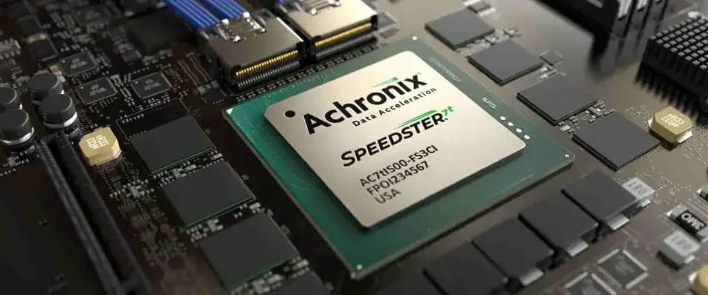
Use the applicable device data sheet, hardware design guide and reference design conditions. Identify supply sequencing, decoupling, unused-pin handling, drive configuration and interface limits. Check that the document applies to the exact part and package revision.
Reference layouts can explain a manufacturer's intended implementation, but differences in board stack, enclosure and interfaces still require review. Treat copied geometry as a starting point with conditions rather than a substitute for the device-specific requirements.
Distinguish edge time from clock frequency
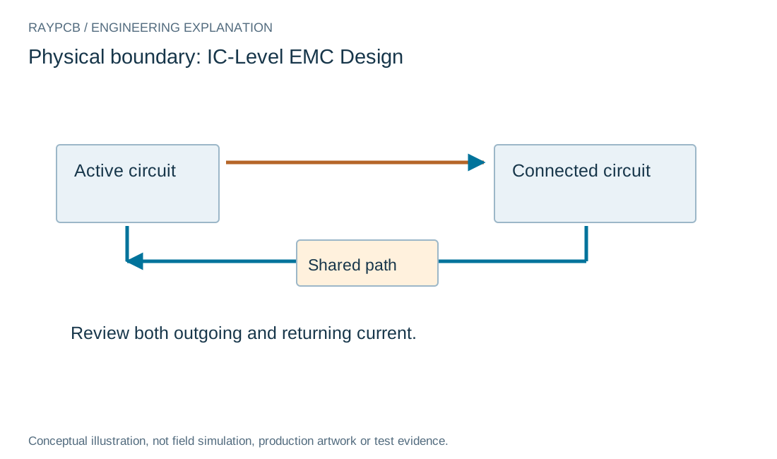
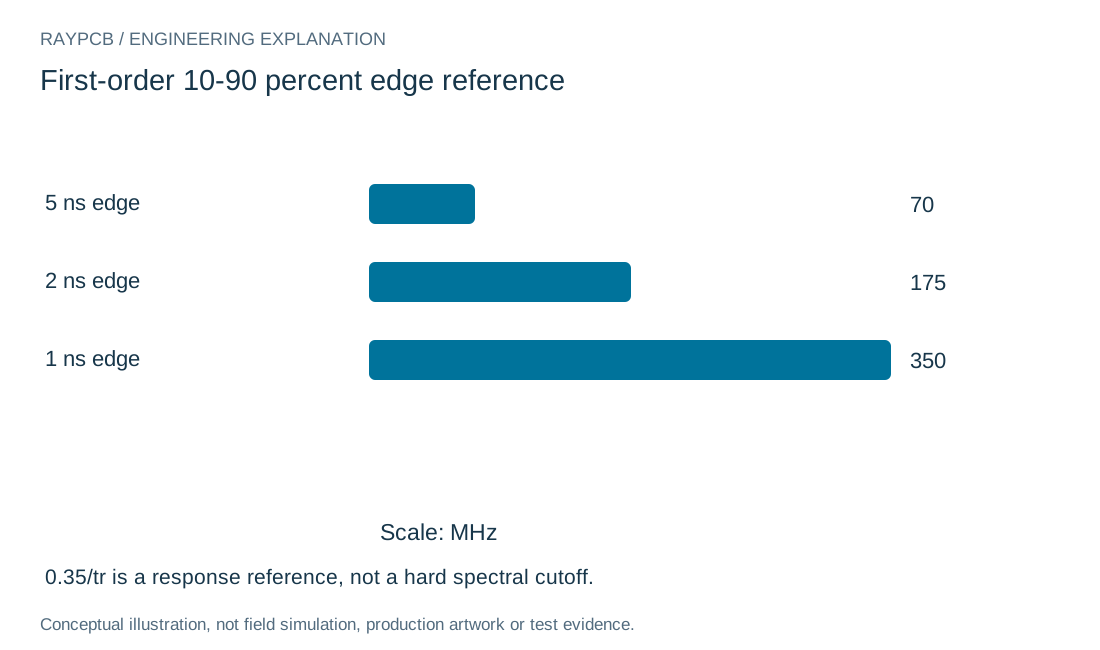
A slowly repeating signal can have a fast transition. The worksheet uses the first-order relation bandwidth ≈ 0.35/rise time. For an illustrative 1 ns rise time, that reference is 350 MHz, even if the repetition frequency is much lower.
This relationship is not a universal emissions cutoff or a substitute for the actual waveform spectrum. Package behavior, overshoot, duty cycle and loading can change the relevant content. Use the result to frame a review of transitions and interconnects, not to claim frequencies above it are absent.
| Review item | What to establish |
|---|---|
| Device applicability | Exact device, package, guide revision and relevant configuration. |
| Transitions | Measured or modeled edge conditions at the intended endpoint. |
| Local current paths | Supply pins, mounted capacitors, vias and return references. |
| Release control | Firmware settings, approved alternatives and revalidation triggers. |
Select drive strength from the interface task
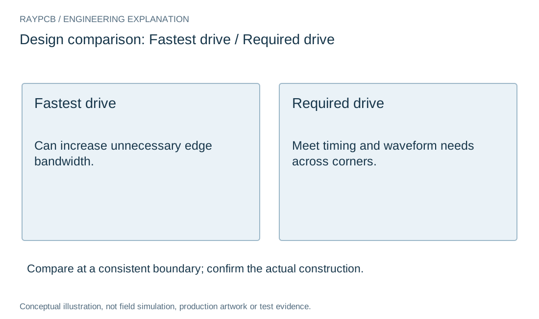
Some devices provide slew-rate or drive-strength controls. Choose settings that meet the receiving interface's timing and voltage requirements with the actual load. Reducing an edge rate can help one coupling mechanism while reducing timing margin elsewhere.
Verify the waveform at the relevant endpoint and retain the configuration setting with the design evidence. A firmware default that changes between builds can alter the electrical behavior even when the PCB artwork remains the same.
Keep switching-current loops local
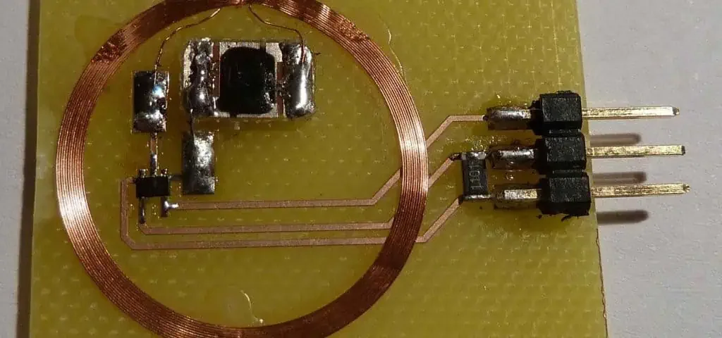
Follow the supply and return loop from the device pins through the mounted decoupling structure. Short geometric distance alone does not establish low loop inductance; via placement, plane transitions and connection geometry also matter.
Use the decoupling placement guide for the mounted-component discussion and the power-impedance worksheet for rail-budget allocation. A capacitor's nominal value does not independently demonstrate a sufficiently low impedance across the required frequency range.
First-order edge bandwidth reference
First-order edge bandwidth reference
Use the current inputs and keep the assumptions
Start with the physical boundary named above the inputs. Enter your own values, or select Load example to explore the labeled teaching case. Example mode remains visible after edits so an illustrative result is not mistaken for measured project data. Clear for my inputs removes the sample values and starts a separate record.
Generate the result after completing the relevant fields. Changing an input invalidates the previous output and disables its download until you calculate again. Read the limitations next to the result: a ratio, margin or checklist does not qualify a channel, approve an EMC test or establish a supplier capability.
Download the current result if it supports your review. The text file contains inputs, outputs, assumptions and the tool version. It stays on your device; attach it manually to an enquiry if useful. No CAD or measurement file is uploaded or interpreted, and nothing is automatically inserted into the Contact form. You can ask an engineering question without completing this tool.
| Input | What to establish before using it |
|---|---|
| Review reference | Nonconfidential scope or revision. |
| 10–90% rise time · ns | Single-pole response assumption for0.35/tr. |
| Clock repetition · MHz | Not the same as edge bandwidth. |
Review pin escape and reference transitions
Pin assignment and escape routing can create return discontinuities or shared paths that affect several signals. Where the device permits flexibility, coordinate the logical assignment with the physical interface. Check package documentation before assuming interchangeable pins or banks.
For an FPGA, the FPGA design review owns bank voltage, configuration and broader bring-up checks. DDR interfaces need their controller-specific routing requirements; those should not be replaced with a general EMC spacing rule.
Treat unused pins and interfaces deliberately
An unused clock output, floating input or unconnected interface can create behavior that is invisible in the intended functional path. Apply the manufacturer's instructions for termination, biasing or disabling. Confirm the state during reset and configuration as well as normal operation.
Do not add pull resistors or filtering indiscriminately. Their values and placement can affect startup, programming or interface timing. Record the reason and applicable device requirement for changes that influence the pin state.
Validate with representative operating modes
Exercise relevant workloads, supply conditions and simultaneous interfaces. A low-activity demonstration may miss switching behavior that appears during a transfer, processing burst or power-state transition. Keep firmware and register settings with the measurement record.
The EMC troubleshooting workflow helps turn a suspicious spectral feature into a controlled investigation. A peak near a clock harmonic suggests an experiment; it does not prove the IC is the only source or that replacing it is the correct remedy.
Release the configuration with the hardware
Include critical register settings, resistor options, supply requirements and approved component substitutions in the release package. Identify which changes require another interface or EMC review. Component procurement decisions should preserve the behavior that was actually evaluated.
For RAYPCB assembly review, provide the exact part numbers, package orientation, approved alternatives and any configuration-dependent inspection instructions. Product compliance remains a system-level conclusion based on the applicable evaluation, not an attribute inferred from an IC brand or a generic board checklist.
Use a source, path and victim record
Describe the disturbance source, its coupling path and the circuit or external system affected. This framework helps choose a testable change. It does not require knowing every field distribution before beginning, but it does require a hypothesis more specific than saying that the board has noise.
Record the product operating mode, software revision, cables, enclosure and power source. A bench configuration that omits those elements can be valuable for isolation, yet should not be mistaken for the final product configuration. Mark temporary diagnostic modifications separately from changes approved for production.
Plan regression checks when a change improves the suspected mechanism. A slower edge, filter, shield or different bond can affect timing, thermal behavior, service access or immunity as well as emissions. Evaluate the relevant tradeoffs before freezing the revised schematic, layout or mechanical drawing.
Turn the design decision into a controlled record. Keep the schematic and layout revision, model source, operating case and requirement together. Distinguish an entered assumption from a supplier nominal value and a measured result. If an important value is missing, record the unresolved question rather than replacing it with a convenient typical number.
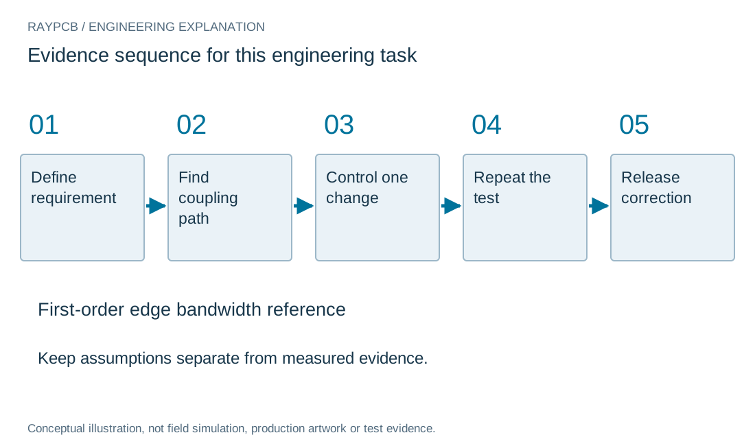
Compare alternatives at a consistent boundary. Preserve the baseline and change one relevant variable when possible. If several features change together, describe the outcome as a comparison between configurations; do not assign the entire improvement to the one component you wanted to justify. Keep both favorable and unfavorable frequency regions in the evidence.
Before a repeat order, check whether substitutions affect the reasoning. A package change, alternate dielectric, shield finish or assembly operation can invalidate an earlier comparison even when the visible board outline is unchanged. Specify which changes need engineering review and which are already accepted. This makes the purchasing and manufacturing handoff useful without asking either team to reconstruct the original electrical investigation.
Standards, source context and limits
Use the applicable device documentation, interface specification and test-method edition for actual requirements. The public sources below explain particular methods; they do not certify the board on this page or replace a licensed standard. Match the document to the selected device, construction and end product before applying a numerical rule.
Numeric examples are teaching inputs unless explicitly identified otherwise. Archive photographs provide physical context, not current factory, customer-project or inspection evidence. Original drawings explain the stated model and are not production artwork, field-solver output or measured waveforms. No search ranking, compliance outcome or manufacturing limit is inferred from these illustrations.
For fabrication scope and the agreed construction requirements, see PCB manufacturing.

