Integrated circuits are essential building blocks powering nearly all modern electronic systems. Various semiconductor devices offer different capabilities and tradeoffs between factors like performance, development cost, and flexibility.
Key categories of ICs include Application-Specific ICs (ASICs), Application-Specific Standard Products (ASSPs), System-on-Chips (SoCs), and Field Programmable Gate Arrays (FPGAs). This article contrasts the key differences between these IC implementation approaches and provides guidance on selecting suitable options for electronics projects.
ASIC Overview
An Application-Specific Integrated Circuit, or ASIC, is a custom silicon chip designed and manufactured for a particular application or function. Some defining traits of ASICs include:
- Fully customized to requirements with tailored circuits
- Very high performance since logic is hand-optimized
- Long development time and high non-recurring engineering costs
- Manufactured by semiconductor foundry
- Amortize high upfront cost over volume production
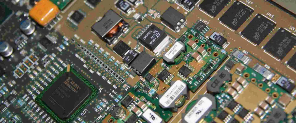
ASICs harness the full power of integrated circuit fabrication technology, packing up to billions of transistors tailored for target applications onto silicon dies less than a square inch. Functions consolidated into ASICs span digital logic, analog interfaces, memory, custom processors, sensors, and mixed signal processing.
Since ASICs are fully designed from the ground up, they entail extensive engineering investment but achieve maximum density, performance, and power efficiency implementing desired functions in silicon. High volume consumer products like smartphones or IoT edge nodes benefit most from custom ASIC solutions.
ASSP Overview
While ASICs target a single specific application, Application-Specific Standard Parts (ASSPs) provide common integrated circuit functions useful across a range of systems. Some key ASSP traits are:
- Standard IC products designed for broad applicability
- Integration improves cost/power/size versus discrete solutions
- Shorter time to market since designs are ready-made
- Limited customization; tailored through external components
- Lower volumes than ASICs; niche vs. mass market
Rather than invest in fully custom ASIC development, ASSPs provide integrated circuits addressing common needs that can be adopted off the shelf with some customization through external passive components, programming, and software drivers.
Examples include codecs, graphics processors, microcontrollers, physical layer transceivers, power management ICs, sensors, wireless radios, and many more. ASSPs are widely used to add intelligence and reduce component count in consumer electronics, IoT endpoints, industrial equipment, automotive, aerospace, medical products, and other embedded systems.
SoC Overview
A System-on-Chip (SoC) integrates multiple functions onto a single silicon die, similar to ASSPs but with greater focus on customer-specific system consolidation. Attributes of SoCs include:
- Complete electronic system integrated into one IC
- Can blend digital logic, analog, memory, processors, etc.
- Extensive incorporation of IP building blocks
- Closer to ASIC than ASSP regarding customization
- Innovation enabler for product miniaturization
SoCs enable fully integrated single-chip solutions tailored for target applications. A smartphone SoC might pack CPU cores, graphics, cellular radios, accelerometers, and other components previously implemented with many discrete ICs.
This system consolidation is achieved by extensive intellectual property reuse. Various processor cores, interface blocks, and subsystems are integrated like LEGO bricks to match requirements while minimizing expensive custom logic.
SoCs occupy a middle ground between ASSPs and full custom ASICs. Their application-optimized integration can enable product breakthroughs by packing entire small electronic systems onto single cost-effective ICs.
FPGA Overview
Field Programmable Gate Arrays (FPGAs) offer an IC alternative maximizing flexibility and rapid prototyping by making logic gates and routing programmable using software. Key FPGA traits are:
- Reconfigurable logic gates and routing
- Programming allows implementing custom hardware functions
- Faster bring-up compared to ASICs with reduced NRE
- No high upfront fabrication costs; sold off the shelf
This reprogrammability makes FPGAs ideal for lower volume products that demand flexibility or require hardware upgradeability. Their architecture is also suited to hardware acceleration and high performance computing applications using inherent fine-grained parallelism.
While not reaching the density or performance limits of fixed-function ASICs, FPGAs empower agile development with reduced costs and risks. Programming follows a structured design flow from concept through synthesis, place and route, and configuration bitstream generation.
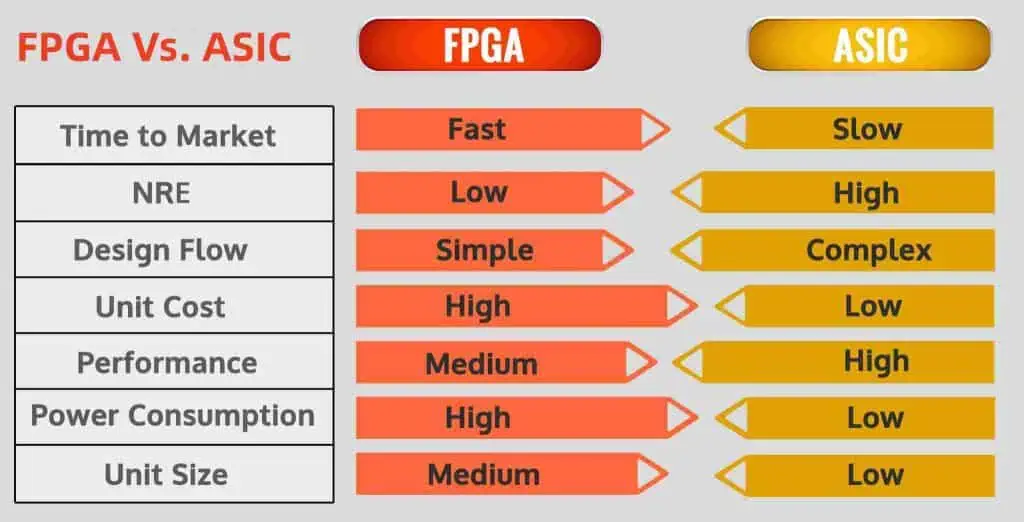
Development Process Comparison
These IC alternatives follow very different development processes and economics:
| ASIC | ASSP | SoC | FPGA | |
|---|---|---|---|---|
| Design Style | Fully Custom | Fixed Function | Mix of Custom and IP | Configurable Fabric |
| Process | 45nm – 7nm node | 28nm – 180nm | 5nm – 65nm | 16nm – 28nm |
| Typical Gate Count | 10M – 5B | 50K – 1M | 5M – 2B | 100K – 5M |
| Development Time | 24+ months | 6-12 months | 12-36 months | 3-12 months |
| Mask Cost | $2M – $5M | $500K | $1M – $3M | Minimal |
| Unit Cost | $1 – $500+ | $2 – $100 | $10 – $150 | $5 – $100 |
| Design Expertise | Full custom IC | System integration | Processor, digital/analog/RF IC | Hardware description language |
| Applications | High-volume consumer electronics, network systems, computing | Broad market horizontal functions | Consumer devices, edge servers, automotive, etc. | Aerospace/defense, instrumentation, networking, acceleration |
ASICs, ASSPs, SoCs and FPGAs each fill particular technology niches based on this range of characteristics.
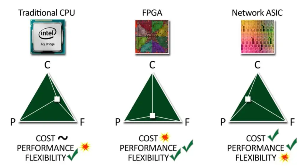
Performance Comparison
The maximum achievable performance follows a tradeoff between flexibility and customization:
| ASIC | ASSP | SoC | FPGA | |
|---|---|---|---|---|
| Logic Density | Highest | Moderate | High | Lowest |
| Speed | Fastest | Fast | Medium | Slowest |
| Power Efficiency | Excellent | Very Good | Good | Poorest |
| Cost at Scale | Lowest | Low | Medium | Highest |
| Design Cost | Highest | Lowest | High | Medium |
| Time to Market | Slowest | Fastest | Medium | Fast |
| IP Reuse | Little | None | Extensive | Moderate |
| Upgradeability | None | None | Moderate | High |
ASICs achieve unparalleled density, speed and efficiency implementing logic in silicon but require immense upfront investment. ASSPs quickly provide known functions but with less custom configurability. SoCs balance integration with some optimization for target applications. FPGAs make iterative hardware development accessible through their configurable architecture.
Application Fit Analysis

Determining the best IC approach involves analyzing product requirements and business factors:
Volume – ASICs only make sense above very high volumes given high fixed costs. ASSPs and FPGAs suit lower quantities.
Performance – When pushing the limits of speed, power or density, custom ASICs have an edge. But often an SoC or FPGA meets needs.
Flexibility – FPGAs allow modifying hardware after deployment. ASSPs offer modest configurability. ASICs are fixed.
Cost – Strongly related to volume. ASSPs minimize cost for modest volumes. ASICs achieve lowest cost at scale.
Time-to-market – ASSPs and FPGAs enable faster product development. ASICs have long lead times.
Design Experience – ASSPs leverage existing designs. ASICs require semiconductor engineering expertise.
Upgrade Cycles – FPGA and flash-based SoCs can evolve in the field. ASSPs and ASICs are fixed at fabrication.
Analyzing these factors helps determine the best IC approach for particular products and markets. Hybrid solutions can combine ASSPs or FPGAs with some custom logic using ASICs or eFPGAs where programmability is still needed after volume production.
Conclusion
ASICs, ASSPs, SoCs and FPGAs each have merits depending on product requirements, markets, and business objectives.
- ASICs provide unmatched performance through customization but require extensive investment only warranted for mass-market consumer devices.
- ASSPs quickly integrate common functions with modest flexibility.
- SoCs deliver application-optimized consolidation blending IP reuse and customization.
- FPGAs maximize prototyping agility with in-field reconfigurability.
Understanding this IC landscape allows architects to select solutions balancing capability, cost, risk, and time-to-market for electronics projects across diverse industries. Advances like design tool automation and fabrication improvements continue expanding the realm of feasible customization. But fundamental tradeoffs remain between flexibility, integration, efficiency, and fixed costs that must be weighed given business constraints.
Frequently Asked Questions
If ASICs offer maximum performance, why aren’t they more widely used?
The extremely high non-recurring engineering costs and development time make ASICs only practical for very high volume consumer products where the massive upfront investment is recouped over millions of units. They are not feasible for lower volume systems.
What are some examples of common ASSP products?
Some widely used ASSPs include microcontrollers, display drivers, image sensors, touchscreen controllers, wireless modems, Ethernet PHYs, power management ICs, USB interface chips, and codecs/DSP audio processors.
Why can’t multiple ASSPs be combined to form a low-cost substitute for an SoC?
Using multiple ASSPs requires PCB area for packaging and interconnects between chips. This increases cost and size while reducing reliability compared to a single-chip SoC solution. SoCs improve integration.
If FPGAs are flexible, why would you ever need an ASIC or SoC?
FPGAs cannot match the density, performance, and power efficiency of either ASICs or SoCs. So for high-volume cost-sensitive products demanding maximum speed or low power, ASICs or SoCs will be superior through customization.
Can a product transition from FPGA to ASIC for production?
Yes, this is a common strategy allowing prototype on FPGA then cost reduce with a fixed ASIC for manufacturing. Some even use structured ASICs or eFPGAs to retain a degree of reconfigurability.