Introduction
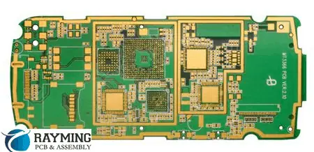
Printed circuit boards (PCBs) form the backbone of all electronic devices providing the platform to mount components and interconnect them. With rapid technological advancements and need for product miniaturization, PCBs have become increasingly complex and crowded. This had led to the growth of high density interconnect (HDI) PCB technology to provide the wiring density needed by advanced electronics.
High density PCBs allow packing of high component densities and fine features into smaller board areas. They enable integration of more functionality into compact and lightweight electronics. HDI capabilities are critical for products like smartphones, wearables, IoT devices, medical equipment etc. that require maximum hardware capabilities within tight space constraints.
This article will provide an in-depth understanding of what constitutes a high density PCB, the key technologies enabling HDI boards and their applications.
What Makes a PCB High Density?

A high density PCB can be defined as a board with:
- Fine trace/space width ≤ 100 μm (4 mils)
- High layer count ≥ 6 layers
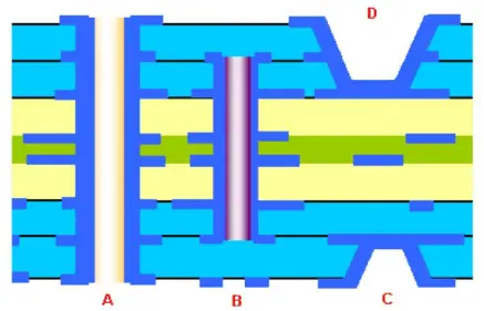
- Blind and buried vias for routing between inner layers
- Microvias with diameters ≤ 150 μm, typically 50 to 80 μm
- High component density with pad/pitch ≤ 0.4 mm
To achieve these high wiring densities, HDI PCBs leverage technologies like laser drilling and imaging of fine features, thinner dielectrics, sequential lamination, and more.
Some key characteristics of HDI boards from standard PCBs are:
| Feature | Standard PCB | HDI PCB |
|---|---|---|
| Line/Space | ≥ 125 μm | ≤ 100 μm |
| Via diameter | ≥ 150 μm | ≤ 80 μm |
| Via pad size | ≥ 350 μm | ≤ 250 μm |
| Layer count | ≤ 12 | ≥ 6, up to 30+ |
| Dielectric thickness | ≥ 50 μm | ≤ 40 μm |
| Solder mask | Liquid photoimageable | Laser direct imaging |
| Finished thickness | ≥ 1.6 mm | ≤ 1.0 mm |
Evolution of High Density Interconnect Technology
The origins of HDI technology can be traced back to the 1980s when traditional PCB fabrication techniques started reaching their limits as circuit densities grew. Some key milestones in the development of HDI are:
- Mid 1980s – Surface mount technology and multilayer boards started gaining adoption to support denser packaging and routing.
- Late 1980s – Microvia technology was developed by IBM allowing connections between layers with small vias. This avoided the need to route lines all the way to the outer layers.
- Early 1990s – Build up layer (BUL) process introduced by Intel-Microsoft consortium to build additional thin signal layers on top of a core board.
- Mid 1990s – Laser direct imaging adopted for fine photolithography to create traces below 25 μm.
- Early 2000s – Stacked microvias and sequential lamination refined the basic HDI processes.
- 2010s – With growth of smartphones, HDI became ubiquitous globally. Lines/spaces dropped below 20 μm.
Continued innovation in materials and processes has enhanced the capabilities of HDI technology to keep pace with market requirements.
Key Technologies Enabling High Density PCBs
A number of advanced PCB fabrication technologies are essential to manufacture the high density boards needed today:
Laser Drilling
Mechanical drilling cannot achieve the 5 mil and lower via sizes seen in HDI. UV lasers are used drill these miniscule vias with high accuracy at tight pitches. Laser also produces cleaner via walls and avoids issues like smear and epoxy clogging faced with small bits.
Thin Dielectrics
Standard glass fabric substrates are too lossy and thick for high speed HDI boards. Teijin’s Nexus and Panasonic’s Megtron 6 are popular low-loss thermoset laminates with dielectric thicknesses down to 25 μm. These allow tighter lines/spaces and prevent signal integrity issues.
Direct Imaging
To fabricate ultra-fine traces below 25 microns, photolithographic methods are used instead of mechanical print-and-etch process. Liquid photoresists are exposed using laser direct imaging to define the circuit patterns with high precision.
Blind and Buried Vias
Blind/buried vias are drilled and plated before lamination of the outer layers, allowing connections between inner layers without consuming routing space. This provides tremendous routing flexibility in HDI designs.
Microvias
These are small vias with diameters typically between 50 to 80 μm drilled with lasers. Microvias connect adjacent layers in HDI boards without using board area.
Build Up Layers
Additional thin dielectric layers are added on either side of the core HDI board using sequential lamination. These provide more routing layers to relieve congestion and integrate components.
Fine Pad/Pitch SMT
To place more components in smaller areas, fine pitch component packaging from 0.4 to 0.15mm pitch is used. The PCB fabrication process must achieve the pad geometries and tolerances needed for this.
HDI Board Construction

There are three fundamental types of HDI board constructions used:
1. Basic HDI
This construction has 4 to 8 blind via layers with at least one fine line top or bottom layer joined by microvias. Blind vias route between internal layers eliminating the need for via stubs. A 25 to 50 μm finish layer can integrate fine pitch SMT components.
2. Complex HDI
Complex HDI boards sandwich very thin core and buildup layers containing microvias between thicker sub-assemblies containing conventional and blind/buried vias for routing density. There can be multiple such sub-assemblies in large boards.
3. Sequential Lamination HDI
Here the core board contains 6 to 12 layers. Then additional build up layers are added sequentially by laminating 25 to 60 μm thin dielectric films. Vias in each layer are stacked to form connections between the layers. Components can be embedded in the outer build up layers.
The choice of HDI construction depends on layer count, component density, routing congestion and other design needs.
Applications of High Density PCBs
Some major application areas where HDI PCB technology provides major benefits are:
Consumer Electronics
Smartphones, tablets, wearables and other compact consumer electronic devices extensively use HDI boards to cram maximum functionality into limited space. The small via sizes help in routing dense chip-scale packages (CSP).
Automotive Electronics
Infotainment systems, advanced driver assistance systems (ADAS) and vehicle control units need HDI boards due to high component densities. Weight and fuel efficiency demands also drive adoption.
Medical Electronics
Medical equipment like imaging systems, patient monitors etc. require HDI PCBs to integrate multi-modality functionality into small, ergonomic and portable devices.
Aerospace and Defense
Avionics, radar and electronic warfare systems use rugged, lightweight HDI boards with high layer counts for excellent signal integrity and noise control in harsh environments.
High-End Computing
Supercomputers, data servers and network switches demand maximum speeds which is enabled by HDI PCBs due to their electrical performance advantages.
Advantages of Using High Density PCBs
Some benefits offered by high density PCBs are:
- Space saving – HDI technology provides 2-4x improvement in component packaging density versus conventional PCBs. This enables product miniaturization.
- Design flexibility – The routing flexibility offered by microvias and additional routing layers accommodates last-minute design changes easily.
- Signal integrity – Electrical performance is improved by allowing shorter traces, matched lengths, tighter layouts and fewer stubs/vias.
- Lower costs – Despite higher initial cost, fewer PCBs are needed so system cost reduces. Overall manufacturing costs also lower due to tiny components.
- Weight reduction – Elimination of wires and backplanes along with smaller components reduces weight significantly for aerospace and portable applications.
Challenges in High Density PCBs
Some key challenges faced in designing and manufacturing HDI boards are:
- Extremely tight tolerances in fabrication require advanced processes and equipment. This increases cost.
- Thermal management is difficult due to high power densities. This requires planning for heat sinks, thermal vias etc.
- High costs of rework due to microvia holes makes designs unforgiving of mistakes.
- Signal and power integrity demands complex analysis and modeling to prevent issues.
- Warpage due to coefficient of thermal expansion (CTE) mismatches in thin multilayers requires careful material selection.
Future Outlook
Emerging applications like Internet of Things (IoT), wearables, electric vehicles etc. will drive greater adoption of HDI technology. Additive manufacturing and substrate-like PCBs will enable embedding of components. Line widths may shrink below 10 μm driven by 5G rollouts. However, fabrication costs and margins will remain challenges for further innovations.
FAQs
What is the key difference between conventional PCB and HDI PCB?
The ability to fabricate fine features like traces below 100 μm and microvias below 150 μm sets HDI boards apart. This provides much higher wiring densities.
Is HDI PCB suitable for analog circuits?
Not usually – the high frequencies and close coupling in HDI boards increases noise pickup and crosstalk. Standard PCBs are generally preferred for analog/mixed signal designs.
Can components be embedded inside HDI PCB?
Yes, additional build up layers can be used to create cavities for embedding bare die, capacitors, resistors etc. This helps further reduce size and enhances electrical performance.
Are HDI PCBs prone to failure due to thinner dielectrics?
With careful handling and component selection, reliability is not compromised. The adhesion between dielectric films is critical however and tested thoroughly during qualification.
How are very small microvias in HDI boards plated?
Specialized techniques like panel plating using a conformal anode are used to achieve uniform plating and void-free copper filling of high aspect ratio microvias.
4 Tips in high-speed (>100MHz) high-density PCB design
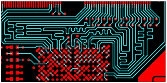
In the case of fixed circuit board size, if more functions need to be accommodated in the design, it is often necessary to increase the track density of the PCB, but this may cause mutual interference of the track to be enhanced, and the track are too thin to make the impedance impossible to reduce. . Pay attention to crosstalk interference when designing high-speed, high-density PCB because it has a large impact on timing and signal integrity. Here are a few caveats:
1. Control the continuity and matching of the trace characteristic impedance.
2. The trace space. The spacing commonly seen is twice the line width. The simulation can be used to know the influence of the trace spacing on timing and signal integrity, and to find the minimum space that can be tolerated. The results may vary from analog chip to chip. Choose the appropriate termination method. Avoid the same running direction of the upper and lower adjacent layers, or even overlap with each other because the crosstalk is larger than that of the adjacent lines in the same layer.

3. Use blind/buried via to increase the area of the track. However, the manufacturing cost of the PCB board will increase. It is really difficult to achieve full parallelism and equal length in actual implementation, but still try to do it.

4. Differential termination and common-mode termination can be reserved to mitigate the effects on timing and signal integrity.
Related posts:
- Top 18 High-Density Interconnect ( HDI) PCB Manufacturers in the World
- Unlocking the Power of Fr4 Density: A Comprehensive Guide
- Why the Arlon 49N PCB Material Is Useful In High Temperature or High Performance Applications
- What Is Panasonic HEPER R-1755D: The High Heat Resistance (High-Tg) Multi-Layer Circuit Board Material?
