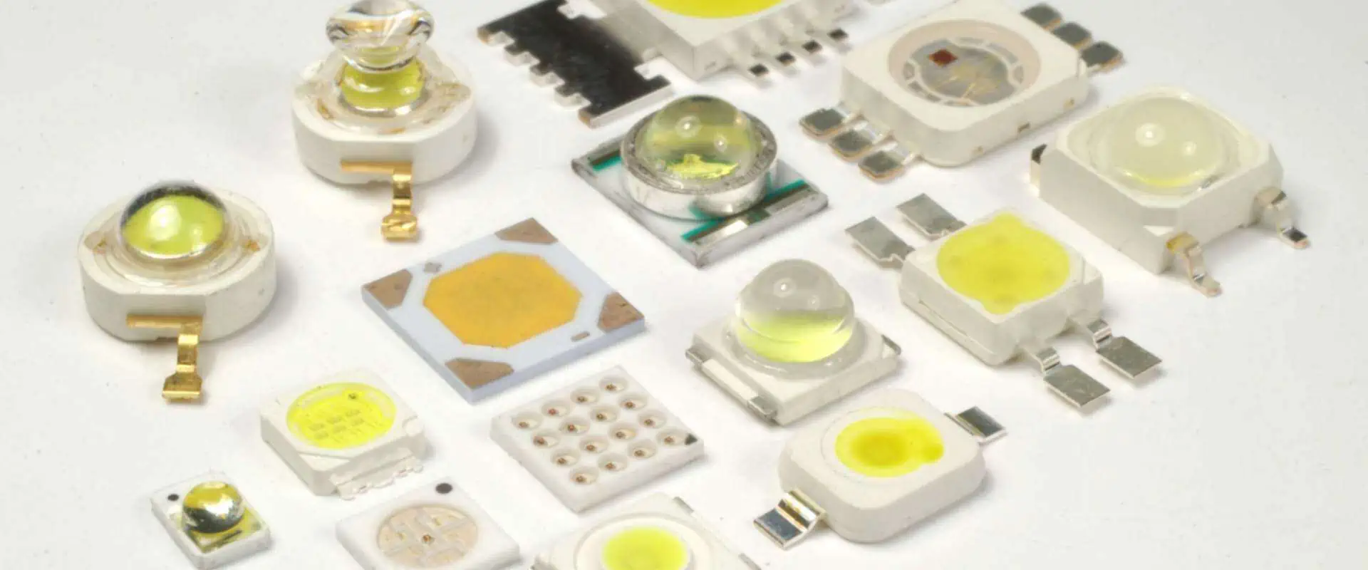
Wi-Fi modules or chips allow electronic devices to wirelessly connect to the Internet or other networked devices using the popular 802.11 Wi-Fi standards. They are widely used in products like smartphones, laptops, smart home appliances, industrial equipment and more.
The core component in a Wi-Fi enabled device is the Wi-Fi module which handles the wireless communication. This article will provide an overview of the key components within a Wi-Fi module and discuss the PCB design principles and layout techniques for implementing Wi-Fi modules to ensure proper functioning.
A Wi-Fi module contains the following key components and sub circuits:
Microcontroller (MCU)
A microcontroller such as ARM Cortex M3 or M4 runs the main firmware that controls the Wi-Fi module functionality. It interfaces with the host system over SPI, USB etc.
Wi-Fi Chipset
The RF chipset with baseband processor handles modulation, encoding, packetization and other signal processing related to the wireless transmission and reception.
Popular Wi-Fi chipsets are Cypress CYW4343W, Microchip ATWILC3000, Texas Instruments WL183x, Realtek RTL8723DS etc. High integration SoCs also combine the chipset with microcontroller.
Power Amplifier
The power amplifier boosts the output from the RF chipset to achieve the required wireless range. There are separate PAs for 2.4GHz and 5GHz bands.
Low Noise Amplifier
The LNA provides initial amplification of received signals with minimal noise. Improves the receiver sensitivity.
RF Matching Network
Carefully designed matching circuits using components like inductors and capacitors match the impedance between the RF ICs/PAs and the antennas. This maximizes signal power transfer.<img src=”https://drive.google.com/uc?export=view&id=1Am9E_9lTg1o7OdnbUGFZbnrSAeqxTNW3″ alt=”WiFi module block diagram” style=”width:500px;height:300px;”>
Oscillators
Precision oscillators provide the required clock signals to the microcontroller and RF chipset. TCXOs (Temperature Compensated Crystal Oscillator) offer stable frequency over temperature variations.
Filters
EMI filters, harmonic filters reduce noise emission and improve signal quality.
Power Management
Voltage regulators and DC-DC converters generate clean power rails from the input supply.
Flash Memory
Stores the module firmware. External serial flash may be used for higher capacity.
PCB Antenna
Printed antennas etched on the PCB itself are commonly used. Or provisions for external antenna connectors.
Indicators
LEDs to provide visual indication of Wi-Fi connectivity status.
Debugging Support
Test points, JTAG/SWD interfaces help debug and program the module.
Host Interface
USB, SD card, SPI etc. interface to communicate with the main host system.
Additional Components
Such as baluns, resistors, capacitors, crystals, buttons, fuses complete the circuitry.
Wi-Fi Module PCB Design Guidelines
The PCB design and layout for a Wi-Fi module is crucial for its functioning and requires careful implementation. The key guidelines are:
Placement
Optimal component placement minimizes track lengths and noise coupling. Group related sub-circuits together with adequate spacing. Keep RF traces short and direct.
Stackup Selection
A 4-layer or 6-layer PCB stackup with adequate copper thickness enables effective shielding, transmission lines and heat dissipation.
Impedance Control
Controlled impedance routing (50Ω or 100Ω) required for RF traces like chipset to connector, chipset to antenna.
Bypassing and Decoupling
Liberal use of bypass/decoupling capacitors next to each IC suppresses noise – typical values are 0.1μF, 1μF, 10μF etc.
Transmission Lines
Controlled impedance lines required from RF ICs to antennas with proper width/space based on stackup. Avoid 90° bends.
Grounding
A continuous ground plane provides low impedance reference. Use several vias to connect ground pads. Have separate analog and digital grounds which join at a single point.
Supply Filtering
Additional ferrite beads, capacitors and pi-filters on supply lines prevent noise coupling.
Shielding
Use coplanar waveguides with ground planes or full copper fills to isolate RF and noise sensitive parts.
Antenna Design
On-board printed antennas like Inverted F, meander line perform adequately for many devices. Provide 50Ω tracks for external antenna connectors.
Thermal Relief
RF ICs dissipate significant heat. Thermal reliefs under pads, copper fills and vias help transfer heat to bottom layer.
Wi-Fi Module Layout Considerations
Here are some key layout techniques that must be followed for a Wi-Fi PCB:
Component Placement
Place components with care for short traces. Keep RF chipset near antenna. Group decoupling caps. Place heat sources on edge near connectors. Have a symmetrical layout.
Routing
Use 45° traces for RF lines. Avoid 90° turns. Do not run RF trace along board edge. Keep RF and digital routes separated. Avoid noise coupling.
Copper Fills
Use copper pours for shielding and heat dissipation. Maintain clearance from traces and pads. Add stitching vias for ground continuity.
Vias
Minimize via stubs. Any open vias should be back drilled. Use caps/epoxy to seal unused vias. Place vias around perimeter of grounds for stability.
Board Shape and Size
Avoid long and thin PCB shapes. Allow margin from edge for manufacturing tolerance and case mounting. Standard rectangular sizes help reduce cost.
Antenna Clearance
Keep clearance below antenna area on bottom layer for optimal radiation. Do not route noisy traces below antenna.
Text Markings
Use smaller text size. Avoid text under components. Place reference designators and markings intelligently to assist assembly and testing.
Wi-Fi PCBs can be fabricated using industry standard process:
Lamination – Metal and dielectric layers are stacked up under high pressure and temperature. 2.4GHz modules typically use FR408 material while 5GHz modules require higher performance RF laminates like Rogers 4003C.
Drilling – Holes are precisely drilled for vias and component mounting. Some RF modules require laser drilling for very small microvias.
Metallization – Electroless copper and direct plate copper create the conductive traces on layers along with plating the drilled holes for interconnection between layers.
Photolithography – Desired track patterns are printed using lithographic techniques. Several alignment steps add more trace layers.
Etching – Exposed unwanted copper is etched away leaving only the protected copper to form the designed circuitry pattern.
Solder mask – The solder mask layer is applied for electrical insulation and mechanical protection with openings left only at points requiring soldering.
Silkscreen – Identifying textual and graphical markings are printed using the silkscreen legend layer.
Routing – Individual PCBs are cut apart from panels using routers or v-score.
Assembly of components on the fabricated PCB comprises:
Stencil Printing – A metal stencil is used to apply the solder paste pattern on pads prior to component placement.
Pick and Place – Surface mount components are accurately placed on pad locations using automated assembly machines.
Reflow Soldering – The PCB passes through the reflow oven thermal profile to form reliable joints by melting the solder paste.
Cleaning – Any post-soldering flux residues are cleaned off to prevent contamination.
Conformal Coating – A protective plastic coating may be applied for environmental protection and preventing short circuits.
Curing – For epoxy-based coatings, a heat cure cycle ensures complete polymerization.
Testing – Comprehensive testing validates RF performance along with electrical functionality and program operation. Failed boards can be reworked.
Certification – Final regulatory certification for emissions, safety compliance etc. needs to be completed.
The assembled Wi-Fi module can then be integrated into the final product enclosure using mounting points, connectors, cables etc.
Conclusion
Wi-Fi connectivity has become an essential feature in many electronic systems today. The Wi-Fi module is the core enabler, housing the RF, baseband and microcontroller components required for wireless communication along with supporting circuitry within a small PCB. Careful schematic design and PCB layout applying the specific guidelines outlined here are crucial to develop a reliable, high performance Wi-Fi board. With the availability of proven RF chipsets and contract electronics manufacturing services, companies can now readily build Wi-Fi capability into their products with speed and cost efficiency. As Wi-Fi standards and chips continue to evolve with higher speeds, greater range and advanced capabilities, efficient implementation using proven PCB design principles will remain key to creating the compact, robust Wi-Fi modules powering tomorrow’s connected world.
FAQs
What are some key factors in choosing a Wi-Fi module?
Key parameters are protocol support, operating frequency, data rates, tx power, sensitivity, interfaces, certifications, power consumption, operating temperature, and packages.
What is the difference between a Wi-Fi chipset and a Wi-Fi SoC?
A chipset consists of separate ICs – one for RF/baseband processing and one for the microcontroller. An SoC integrates both functions into a single chip.
How much does a Wi-Fi module typically cost?
Simple Wi-Fi modules with PCB antenna can cost under $5. High performance multiprotocol combo modules with precertification can cost $15-$20 or more.
What kind of testing is required for Wi-Fi modules?
Important tests are frequency/channel accuracy, modulation quality, tx power, rx sensitivity, bandwidth, error vector magnitude, interference handling, security, and regulatory compliance.
What are some key PCB design tools used for Wi-Fi layouts?
Allegro PCB Editor, Mentor Xpedition, Cadence Allegro/OrCAD, Altium, and Zuken CR-8000 are some leading PCB design platforms.
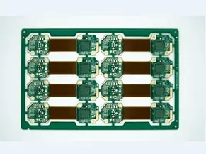
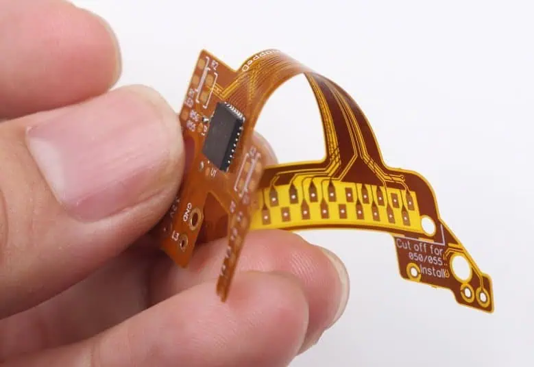
Rigid-flex PCBs provide the ability to integrate multiple rigid PCBs interconnected using flexible circuits in a single assembly. The combination of rigid and flexible materials in one board allows three-dimensional packaging and increased component density within electronic devices.
6 layer rigid-flex refers to a board stackup with 6 conductive copper layers. This article will provide an overview of 6 layer rigid-flex PCB technology covering:
Benefits and applications
Construction and materials
Fabrication process
Design guidelines
Assembly considerations
Cost impact
Benefits of 6 Layer Rigid-Flex PCBs
Compared to conventional rigid boards, 6 layer rigid-flex PCBs offer the following advantages:
Increased Component Density
Folding rigid sections vertically allows placing components on both sides of stacked boards for space and height reduction.
Simplified Assembly
Replacing discrete flexible cables and wire harnesses with integrated flexi-rigid board reduces assembly labor and errors.
Enhanced Flexibility
Eliminates inter-board connectors by running flexible circuits between rigid sections. Accommodates complex motion paths.
Improved Serviceability
Modules can be independently removed for repair/upgrade without affecting other sections by separating along flex bends.
Reduced Weight
Inter-board cables have heavier insulation than thin flexible layers.Removes extraneous housing needed for discrete cables.
Lower Costs
Fewer connectors, simpler assembly, higher density save on materials cost and manufacturing expenses.
Signal Integrity
Better high speed performance by minimizing discontinuities through maintained impedance in traces spanning rigid and flex sections.
Reliability
Avoids reliability risks associated with external wiring and interconnections.
Applications of 6 Layer Rigid-Flex PCBs
The unique capabilities of rigid-flex make them ideal for the following applications which require packaging density, versatility and reliability:
6 layer rigid-flex technology provides adequate routing channels to implement complex high density circuits for such miniaturized and high performance products.
Rigid-Flex PCB Construction
6 layer rigid-flex consists of:
Multiple layers of copper clad rigid FR-4 material
Layers of adhesive-based flexible dielectric like polyimide
Coverlay bonding the flexible layers
The main rigid section has 6 copper layers. The flex sections integrate 2-6 layers depending on routing needs. Sections are held together by an adhesive. Plated thru holes provide interconnects between layers.
Rigid sections provide mechanical strength for component mounting and heatsinking. Flex layers enable out-of-plane motion and 3D assembly. Different rigid and flex materials can be combined for optimal electrical and thermal performance.
Components are only assembled in rigid sections. Flex area is left unpopulated.
Sufficient clearance should be maintained around component pads close to flex joints.
Adhesives help strengthen the joint between rigid and flex sections.
Careful hand soldering is needed near bends to prevent damage from stress.
Strain relief methods provide support against flex damage during motion.
Conformal coating increases reliability by preventing moisture ingress through the flexible layers.
Manual inspection of assembled boards is advised to detect any cracks or breaks.
Cost Impact
Rigid-flex PCBs have a higher fabrication cost compared to conventional rigid boards due to:
Additional process steps involved
Specialized materials like adhesives and flexible dielectrics
Lower panel utilization
Increased scrap rate
Manual operations for stacking and lamination
However, the ability to integrate multiple PCBs far outweighs the marginal increase in individual board cost in most applications. Assembly cost reduction also offsets the higher board cost.
For 6 layer rigid-flex PCBs, fabrication cost is approximately 1.8 to 2 times the cost of a similar 6 layer rigid PCB.
Conclusion
6 layer rigid-flex PCB technology provides design flexibility to integrate multiple PCBs interconnected using flexible circuits within a single compact assembly. The combination of standard rigid board fabrication processes and flex circuit manufacturing technologies enables reliable construction of multilayer rigid-flex boards. Careful design planning is needed to effectively utilize the benefits while accounting for assembly and long term reliability. With their ability to package disparate components in close proximity, rigid-flex PCBs offer system level benefits like increased density, reduced weight, faster assembly and improved serviceability. As electronic devices continue getting more compact and complex, the unique value proposition of multilayer rigid-flex PCBs will see them being adopted across industries for a variety of demanding applications.
FAQs
What are some key differences between rigid-flex vs flexible PCBs?
Rigid-flex combines both rigid and flexible circuits. Flex PCBs contain only flexible layers. Rigid-flex provides structural stability with flexibility while flex PCBs are solely meant for dynamic flexing applications.
What design tools are used for rigid-flex PCBs?
Specialized rigid-flex CAD tools like Mentor Xpedition, Altium, Cadence, Zuken are preferred. Separate rigid and flex profiles are generated and then combined.
Can component mounting across both rigid and flex areas be accommodated?
Component mounting on flex areas is not recommended since they cannot withstand soldering stresses and will crack. Components should be mounted only on rigid sections.
How many flex layers are typically used?
2 to 4 flex layers are common for interconnects between rigid sections. If more traces are required, additional flex layers can be added.
What are thermal reliefs in rigid-flex boards?
Thermal reliefs are cutouts below component pads and vias to reduce conducted heat transfer into the flexible region which has lower thermal tolerance.
RayMing is a 2 layer flexible PCB manufacturer, flexible printed circuit boards (PCBs) have become increasingly popular due to their versatility and space-saving properties. Among these, the 2 layer flexible PCB stands out as a common and cost-effective solution for many applications. This article will delve into the intricacies of 2 layer flexible PCBs, covering their design, manufacturing process, cost considerations, and applications.
What is 2 Layer Flexible PCB?
A 2 layer flexible PCB, as the name suggests, is a flexible circuit board that consists of two conductive layers. These layers are typically made of thin copper foils, separated by a flexible dielectric material. The flexibility of these PCBs allows them to be bent, folded, or shaped to fit into tight or unconventional spaces, making them ideal for a wide range of electronic devices.
Key Features of 2 Layer Flexible PCBs:
Flexibility: Can be bent or folded to fit various form factors
Lightweight: Significantly lighter than rigid PCBs
Space-saving: Ideal for compact electronic devices
These tools often include specific features for flexible PCB design, such as 3D modeling capabilities to visualize bends and folds.
Cost Estimate of 2 Layer Flexible PCB
The cost of 2 layer flexible PCBs can vary significantly based on several factors. Understanding these factors can help in estimating and optimizing costs.
Factors Affecting Cost:
Board Size:
Larger boards generally cost more due to increased material usage
Material Selection:
High-performance materials like polyimide increase costs
Standard FR4 flexible materials are more cost-effective
Copper Weight:
Thicker copper increases cost but may be necessary for some applications
Production Volume:
Higher volumes typically result in lower per-unit costs
Surface Finish:
ENIG (Electroless Nickel Immersion Gold) is common but more expensive
HASL (Hot Air Solder Leveling) is a more cost-effective option
Design Complexity:
Complex designs with many components or tight tolerances increase cost
Cost Estimation:
While exact costs vary by manufacturer and specific requirements, here’s a rough estimate:
Small quantity (1-10 pieces): 50−50−200 per board
Medium quantity (100-500 pieces): 10−10−50 per board
Large quantity (1000+ pieces): 5−5−20 per board
It’s always recommended to get quotes from multiple manufacturers for accurate pricing.
How is 2 Layer Flexible PCB Made
The manufacturing process for 2 layer flexible PCBs involves several steps, each crucial to the final product’s quality and performance.
Manufacturing Process:
Material Preparation:
Selection and cutting of flexible base material (e.g., polyimide)
Lamination:
Bonding of copper foils to both sides of the dielectric material
Imaging:
Application of photoresist
Exposure to UV light through a photomask to create the circuit pattern
Developing:
Removal of unexposed photoresist
Etching:
Removal of unwanted copper, leaving only the circuit pattern
Coverlay Application:
Application of protective coverlay or solder mask (if required)
Drilling:
Creation of holes for vias and component mounting
Surface Finish:
Application of chosen surface finish (e.g., ENIG, HASL)
Improved reliability in high-vibration environments
Weight reduction in aerospace and portable devices
Enhanced heat dissipation in high-power applications
Conclusion
2 layer flexible PCBs offer a versatile and cost-effective solution for many electronic applications. Their unique properties allow for innovative designs in compact spaces, making them invaluable in industries ranging from consumer electronics to aerospace. By understanding the design considerations, manufacturing process, and cost factors, engineers and product designers can effectively leverage the benefits of 2 layer flexible PCBs in their projects.
As technology continues to advance and miniaturization becomes increasingly important, the demand for 2 layer flexible PCBs is likely to grow. Their ability to combine flexibility, durability, and performance makes them an excellent choice for modern electronic devices, ensuring they will remain a crucial component in the electronics industry for years to come.
High performance and complex PCB designs often involve combining different laminate materials within a single circuit board stackup. A popular hybrid configuration uses standard FR-4 glass epoxy along with high frequencyRogers dielectric material in specific layers.
A 12 layer hybrid PCB with Rogers laminate and FR4 allows optimizing electrical performance and cost. This article provides an overview of hybrid 12 layer PCB stackups with Rogers and FR4 covering design, material selection, fabrication, applications and cost considerations.
Benefits of Rogers + FR4 Hybrid PCBs
Key advantages of using Rogers laminates selectively in a 12 layer FR4 PCB:
Signal Integrity: Provides tightly controlled impedance for high speed signals on Rogers layers
EMI Reduction: Rogers material has lower loss which improves signal quality and reduces EMI
Thermal Management: Higher thermal conductivity dissipates heat from high power components
Mechanical Stability: Rogers material has a lower Z-axis CTE providing enhanced structural stability
Selective RF Performance: High frequency analog circuits can be fabricated on Rogers layers
Cost Savings: Using Rogers only in essential layers with FR4 for rest reduces cost versus full Rogers stackup
Typical Stackup Configuration
A common 12 layer hybrid PCB stackup configuration is:
The higher performance Rogers 4350B material is used in the critical signal layers at the center of the stackup while standard FR-4 handles the rest of the routing.<img src=”https://drive.google.com/uc?export=view&id=1PUosbPyuqbxT-ShQLuKNy Tem5MCyA4GX” alt=”Rogers FR4 Hybrid Stackup” style=”width:300px;height:400px;”>
The exact layer distribution can be adjusted based on high speed and RF routing needs. Additional Rogers layers can be added near the surface for RF components requiring tight impedance control. Simulations help optimize the hybrid stackup configuration.
Rogers vs FR-4 Material Properties
Rogers 4350B offers better electrical and thermal performance than FR-4 but at a higher cost:
Rogers RF laminates allow reliable performance for circuits up to 77GHz. They are available in a range of dielectric constants from 2.2 to 10.2 to suit different applications. Popular alternatives are Rogers 4003C and 5880.
The integration of Rogers material in high layer count PCBs along with FR4 provides a robust solution for products requiring speed, precision and RF performance without the cost of using exotic dielectrics exclusively.
Cost Analysis
For a 300mm x 400mm board, a cost estimate comparison between full FR-4 and hybrid construction in 5000 piece prototype volumes:
Configuration
12L Full FR4
12L Hybrid (Rogers in L5/L12)
Fabrication
$130
$160
Material
$155
$195
PTH Plating
$210
$250
Mask +Legend
$130
$145
Handling
$55
$60
Test
$125
$150
Total/board
$805
$960
The hybrid option with Rogers in 2 layers has around 20% higher cost. But the performance gain outweighs this cost premium in many high speed and RF applications.
Combining Rogers laminates and FR4 dielectric in a 12 layer PCB provides an optimized tradeoff between performance and cost. The integration of high frequency Rogers material in the core layers offers precision routing for signals demanding tight impedance control, low loss and crosstalk isolation within a reliable, industry-standard 12 layer FR4 multilayer board. With careful design planning andworking with fabricators experienced in hybrid multilayer constructions, the Rogers-FR4 hybrid approach enables modern PCBs to implement demanding applications in networking, communications, defense, instrumentation and other leading edge fields.
FAQs
What are some key benefits of using a hybrid PCB stackup?
Hybrid stackups allow optimizing electrical performance, thermal management, stability, density and cost by combining different materials selectively as per circuit needs.
What precautions are required when soldering hybrid PCBs?
Use a lower temperature solder alloy to avoid damaging the higher performance dielectric material. Ramp down temperatures slowly after reflow.
Can components be placed across Rogers-FR4 junctions?
This is not recommended as thermal stresses can induce cracks or delamination. Components should be fully placed over one material.
How are impedance matched traces implemented in hybrid PCBs?
Matching is achieved by using different trace widths on each dielectric layer according to the material dielectric constant. Transitions between widths can be tapering or abrupt.
What are thermal reliefs used for in hybrid boards?
Cutouts below pads and vias facilitate heat transfer into the higher thermal conductivity plane layers while limiting conduction into the outer layers.
8 layers Printed circuit board is generally installed into compact devices that have very restrict requirements of spacing, such as laptop motherboard, communication backplane, wearable watch etc. Due to its complexity and high cost of manufacturing, your 8 layers PCB fabrication should be handled by a reliable and experienced manufacturer. RayMing particularly targets on high-end PCB Manufacturing and assembly services for 10 years and a variety of customers witness the good quality and outstanding services. Our advanced production lines and responsive team would make you stay comfortable without any hassle since you place the order to us.
8-Layer PCB Stackup Selector
8-Layer PCB Stackup Selector 8L
Configure layer thicknesses for high-density 8-layer PCB designs
1.0mm: High-density mobile/wearable 1.6mm: Standard multilayer (most common) 2.0mm: Industrial, automotive 2.4mm: Power systems, thick copper
⚡ 8-Layer Design Tips
Signal Integrity: L3 & L6 are shielded by adjacent planes – ideal for high-speed signals. Power Distribution: L4 & L5 form a tightly-coupled power/ground pair – excellent for decoupling.
The 8-layered Prototype FR-4 PCB is a circuit board with 8 layers that are stacked firmly together with predefined and dependable mutual connections between the layers. An 8 layer FR-4 PCBs has more complex structure. Twisted Traces is a reputable name in the field of manufacturing 8 layer prototype PCBs.
1. It has multiple power and ground planes- a digital ground plane helps prevent noise coupling. 2. It provides more planes for shielding signals from other signals on adjacent layers 3. More layers aid in routing signals that need matching 4. For analog signals especially those with RF, isolation and impedance control on traces is needed.
8 Layer PCB Instant Quote
In terms of a custom printed circuit board, our 8 layer PCB Instant Quote is the fastest turn-time at the best price that we have to offer. For on-demand pricing and ordering for your next printed circuit board project,Get Fast Quote you can contact our online customer support , or send email to sales@raypcb.com , Get 8 Layer PCB Quote Now !
With the constant development in the electronics industry, there has been improvement in PCBs manufacturing. This development has pushed PCBs towards increasing demands such as high speed, reliability, miniaturization, and better functionality which lead to the fabrication of multilayer PCBs. Multilayer PCB are available in different layers which include 4 layers, 6 layers, 8 layers, 10 layers, etc.
These PCBs consist of prepreg and double-sided or single PCBs that are stacked together to produce multilayer PCBs via a predefined mutual connection between them. 8 layer PCBs have gained popularity in different fields due to their exceptional electrical and mechanical properties.
What is an 8 layer PCB?
8 layer pcb manufacturer
An 8 layer PCB is a type of multilayer PCB that provides ample routing space for applications that need multiple power islands. This printed circuit board can help to enhance EMC performance by the addition of two planes.
This board is often mounted on compact devices like motherboard, wearable watch, backplane, etc. The increase in the cost of 8 layers PCB justifies the cost increase to achieve great EMC performance. An 8-layer PCB stackup is made up of four planes and four wiring layers connected by seven rows of dielectric material.
This PCB features a six-layer board with improved EMC performance. An 8-layer PCB is sealed with a solder mask at the bottom and top.
The type of material an 8 layer PCB stackup consists of determines its performance. Thus, you need to be careful when choosing materials during the production process. To produce high-performance PCB, the best materials are substrates and conductive materials.
Substrates
Substrates like glass-epoxy materials help to insulate heat and signals. This helps you to handle the stackup better even in applications with high temperatures. Substrate materials have a great glass transition temperature that maintains the solidness of the PCB stackup.
Conductive materials
Copper is the most effective conductive material utilized in the fabrication process of the layer stackup. This material is an ideal option since it is a good conductor of heat, allowing proper signal transfers and minimizing heat accumulation on the device. Copper is also a cheaper alternative to other materials like silver and gold which are very expensive.
Advantages of 8 Layers PCB Stackups
8 layer PCB stackups offer a number of benefits which makes them an ideal alternative to other circuit board materials. Below are the advantages of these PCBs;
Minimize vulnerability: 8 layers PCBs reduce the vulnerability of a device, hence, increase the overall performance. This helps to shield the internal layers from noise, thereby reducing its vulnerability to external forces.
Reduce Radiation: This type of multilayer stackup helps to get rid of any radiation that might occur in high-speed applications. Unlike other stackups, 8 layers PCBs get rid of electromagnetic interference radiation.
Reduce the cost of operation: 8 layers PCB stackups are a cost-effective option. As regards replacements and cleaning, this stackup saves a lot of money. This means that an 8-layer PCB stackup requires low maintenance and is very durable.
Increase functionality: Opting for an 8-layer PCB will help to improve the speed and functionality of the devices they are used for. This printed circuit board is more reliable and functional in different applications. This PCB features over 4 layers of conductive materials that enhance the signal traces.
Applications of the 8 layer PCB Stackup
The 8 layer PCB stackup is the commonest type of stackup used in most appliances. This multilayer PCB is functional in several applications such as;
Factors that Determine the Cost of an 8 Layer PCB Stackup
The fabrication of an 8 layer stackup costs money and there are several factors that contribute to cost. This type of multilayer PCB stackup goes for about $3, however, certain factors determine the price.
Size of the board: The printed circuit board’s size has to do with the components in it. When there are more components on the board, the size of the PCB will increase. An increase in size will result in an increase in the fabrication cost of the circuit board.
Type of finish: This is another factor that contributes to the cost of an 8 layer PCB stackup. There are several finish options, so the type you choose will determine the PCB cost. Finishes like HASL, ENIG, ENEPIG, and IMM Sn are some of the popular finishes available.
Thickness: The thickness of a circuit board has to do with the materials that enhance the strength of the board. The thicker a circuit board is, the higher its price. The type of materials used in designing the PCB can determine the thickness of the board.
Size of the holes: If the board requires more holes, the cost of design and manufacturing will increase. Thinner holes will require more work before the circuit board can be produced.
Custom specifications: If you request specific configurations for your PCB design, this will increase its cost. More demands for configurations and customizations often increase the cost of producing circuit boards.
Guidelines for a Standard 8-Layer PCB Stackup
It is important you understand that some guidelines need to be met to achieve better performance. If you want a board that delivers better performance, there are guidelines that help you achieve that.
Proper routing direction: For an 8 layer stackup, the application requirements determine the number of layers of signal layers. In a case where there are six signal layers, there must be a perpendicular routing for the signal traces on the adjacent layers. This helps to reduce crosstalk, signaling the significance of various signal routines on the layer stackups.
Ground planes alignment: When the ground planes are split it may result in discontinuity of impedance. The components on the external layer must have extremely low impedance. Also, the components must connect to the internal ground planes through the vias.
Proper return path: You must ensure that the return paths are short enough to eliminate interaction with other components on the PCB.
Buried or blind vias: Another option to consider is utilizing blind or buried vias which will maximize the available space for component routing. You must ensure that you can place the blind via on the board.
The design process of a standard 8-layer PCB starts with a working design. This means that you should determine the type of 8-layer stackup you intend to use. This process will help you achieve a good stackup.
Creation of Idea
First things first, you need to determine the type of 8-layer PCB you need. You can then look for the best way to ensure the PCB stackup works. Select designing software you can use in the designing process. After that, develop a schematic i.e the PCB blueprint.
After developing a schematic, you will add every single piece of information you want to the stackup. The designing process will start with a blank page on the designing software.
Inclusion of component
You will start the designing process by including all the required details on the stackup. Specify the stackup’s shape and the number of layers. Then, you will ink all the details on the schematic. Ensure you review all information on the design and change what is necessary.
Then, you must define the designing rules and be certain that you follow them in the designing process. Don’t take any of these rules for granted so that it won’t affect the stackup’s performance.
Placement of component: At this stage, you will have to determine where other components will be placed. You will also have to determine how to arrange the layers and position drill holes. After this, all the route traces on the stackup will be positioned and then add labels and identifiers. Doing all of these will help you produce the HDI PCB design.
Frequently Asked Questions
What type of vias can be utilized in an 8-layer stackup?
There are different types of vias you can utilize in this type of multilayer stackup. These vias include buried vias, through-hole vias, vias in pads, microvans, and blind vias.
What kinds of surface finishes can be applied on an 8-layer PCB stackup?
In recent times, the 8-layer PCB stackup has become popular. It is important to know that the application of this multilayer stackup is increasing over time. Opting for an experienced 8 layer PCB manufacturer is vital. They will offer you the best stackups that suit your application requirements.
An 8-layer PCB increases the working speed of complex appliances. This stackup improves the signal integrity of various designs. The design of an 8 layer PCB might take some time due to its complexity. An 8 layer PCB manufacturer must be well-detailed to create a good design.
Printed circuit boards (PCBs) have evolved from simple single or double layer boards to complex multilayer boards with 6 or more layers to accommodate increasing component density and interconnectivity needs. 6 layer PCBs provide more flexibility for routing, plane separation and enable partitioning of circuits across layers.
However, designing the 6 layer stackup requires careful planning to utilize the layers effectively and avoid signal integrity issues. Key considerations include layer sequence, reference planes, material selection, copper weights, trace routing and via design. This article provides a detailed overview of 6 layer PCB stackup configurations, thickness calculations and manufacturing processes.
6-Layer PCB Stackup Selector
6-Layer PCB Stackup Selector 6L
Configure layer thicknesses for your 6-layer PCB stackup
1.0mm: High-density, compact designs 1.2mm: Standard thin multilayer 1.6mm: Most common thickness 2.0mm: Power applications, thermal management
⚡ Layer Arrangement Tips
L2 (GND) & L5 (PWR): Place planes adjacent to outer signal layers for better impedance control and EMI shielding. L3 & L4: Inner signal layers – route high-speed signals here for protection.
6 Layer PCB Stackup Configuration
6 Layer PCB Stack-Up
The 6 conductive copper layers in a multilayer PCB are arranged in a predetermined sequence along with dielectric materials separating them. This is referred to as the layer stackup. Some key guidelines for 6 layer stackup design:
Layer Sequence
The conductors are numbered sequentially with the topmost layer being Layer 1. A typical 6 layer board stackup has:
Layer 1: Top/Component layer
Layer 2: Reference plane 1
Layer 3: Signal/Plane layer 2
Layer 4: Signal/Plane layer 3
Layer 5: Reference plane 2
Layer 6: Bottom layer
The top and bottom layers are used for component placement and routing. The inner layers are used for signals and reference planes.
Reference Plane Placement
The reference planes (ground and power) should be adjacent to routing layers for controlled impedance. A continuous ground plane next to signals is highly recommended.
Plane Splits
Reference planes can be split into analog and digital power sections to provide clean isolated supplies to sensitive analog circuits.
Symmetry
Symmetrical arrangement with reference planes above and below the mid layer provides optimal signal integrity. Asymmetrical stackups also used when needed.
Signal Routing
Route critical high speed or noise sensitive signals on inner layers sandwiched between planes. Avoid routing them on outer layers.
Breakout Vias
Use breakout/stub vias when routing inner layer traces to outer layers. Confines any stub effects.
The overall thickness of a 6 layer PCB depends on:
Copper layer thickness
Dielectric layer thickness
Number of lamination cycles
Copper Layer Thickness
Typical copper weights:
Outer layers : 1 oz (35 μm)
Inner layers: 1 oz or 0.5 oz (18 μm)
Plane layers: 2 oz (70 μm) recommended
Heavier copper allows higher current carrying capacity.
Dielectric Layer Thickness
Typical dielectric layer thickness:
8 mil to 14 mil per layer
112-170 μm glass epoxy FR4 material
Thinner dielectrics help minimize layer to layer capacitance
Lamination Cycles
A 6 layer board can be fabricated by:
2 lamination cycles - Bottom 3 layers pressed first, then top 3 layers
3 lamination cycles - Bottom 2, mid 2 and top 2 layers bonded
2 lamination cycles results in lower thickness variation versus 3 cycles.
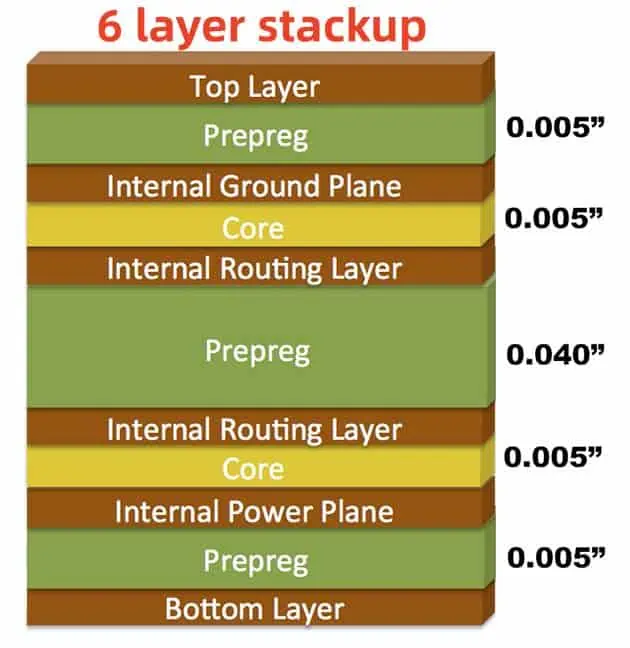
Example 6 Layer PCB Stackup Thickness
Here is a sample 6 layer PCB stackup with typical thickness values:
Copy code
Layer Type Thickness Layer 1 - Top Signal 1 oz (35 μm) Layer 2 Ground 2 oz (70 μm) Layer 3 Signal 1 oz (35 μm) Layer 4 Signal 1 oz (35 μm) Layer 5 Power 2 oz (70 μm) Layer 6 - Bottom Signal 1 oz (35 μm) Dielectric 10 mil (254 μm) Total Thickness 6 Layers 110 mils (2.79 mm)
This is a symmetrical arrangement with approximately 110 mils (2.79 mm) total board thickness. Thinner dielectrics or copper can be used to reduce overall thickness. 8 layer boards typically range from 130 mils to 200 mils thickness.
6 Layer PCB Design and Manufacturing Process
The typical workflow for assembling a 6 layer PCB is:
Some of the key benefits of using 6 layers versus 4 layers:
Additional signal layers for routing dense designs
Ability to segregate power and ground planes
Inner signal layers shielded from EMI/noise
Controlled impedance environment for high speed signals
Flexible power distribution to circuits
Handles greater component density
Overall smaller board footprint area
However, 6 layer PCBs have higher fabrication cost and complexity versus 4 layer boards. The additional layers should be leveraged judiciously from a design perspective to maximize the advantages.
Guideline for Selecting 4 Layer vs 6 Layer
Here are some criteria to decide between 4 and 6 layer boards:
Consider 4 layers for:
Low-mid complexity designs
Smaller board size < 150 cm2
Only 2 or 3 major voltage domains
Lower signal speeds < 1 Gbps
Standard density interconnects
Cost sensitive applications
Consider 6 layers for:
Complex, dense component layouts
Larger board area >200 cm2
Multiple power domains and levels
High speed signals > 2 Gbps
Sensitive analog and RF circuits
Easy routing of traces on inner layers
Looser impedance control requirements
Conclusion
Designing an optimal 6 layer PCB stackup requires careful planning to utilize the layers effectively. Key considerations include selecting the right symmetrical or asymmetrical arrangement, intelligent plane splits, optimal dielectric materials, and routing critical signals on inner layers. Following sound stackup, impedance and routing guidelines helps utilize the full capabilities of the 6 layer board. The fabrication process also necessitates strict process controls to bond and pattern the multiple layers reliably into the finished PCB. With growing complexity and higher performance requirements, 6 layer PCBs are becoming the norm for many advanced designs today.
Frequently Asked Questions
Q1. What are the typical dielectric materials used in a 6 layer PCB?
Some commonly used dielectrics in 6 layer PCBs are:
A 4 Layer PCB (Printed Circuit Board) is a type of multilayer PCB that consists of four distinct conductive layers separated by insulating material. This design offers a balance between complexity and cost, making it a popular choice for many electronic applications.
Structure of a 4 Layer PCB
Top Layer: This is the outermost layer where components are typically mounted. It’s used for signal routing and component connections.
Inner Layer 1: Often used as a ground plane, providing a low-impedance return path for signals.
Inner Layer 2: Typically used as a power plane, distributing power throughout the board.
Bottom Layer: The second outer layer, also used for component mounting and signal routing.
These layers are separated by insulating material, usually FR-4 (a type of fiberglass epoxy resin).
Route all critical high-speed signals on L1. These signals benefit from the solid ground reference on L2, ensuring controlled impedance and minimal EMI.
🟢 Layer 2 – Keep Solid
Never route signals on L2. Every trace creates slot antennas and forces return currents to take longer paths. Keep as 100% solid copper pour.
🔴 Layer 3 – Power Splits
When splitting for multiple voltages, use star topology. Keep splits away from high-speed signal paths to avoid return path discontinuities.
🟣 Layer 4 – Secondary Routing
Use for low-speed signals and power traces. Route perpendicular to L1 traces when possible. L4 signals reference the power plane on L3.
Signal Type
Width
Spacing
Layer
Notes
Standard Digital
4-6 mil
4-6 mil
L1, L4
General purpose
High-Speed (>100MHz)
5-6 mil
2× width
L1
Match impedance target
Differential Pairs
Per calc
Per calc
L1
Length match within 5 mil
Power Traces
20-50 mil
10+ mil
L1, L4
Size for current
Via Strategy
Through-hole vias (0.3mm drill): Use for all standard connections. Always place a ground via within 0.5mm of any signal via to provide return path. Use via stitching around board perimeter for EMI control.
Cost Optimization Tips
Reduce manufacturing costs without sacrificing quality
Parameter
Standard (Low Cost)
Advanced (Higher Cost)
Cost Impact
Trace/Space
4/4 mil
3/3 mil
+25-40%
Via Drill
0.3mm
0.2mm laser
+30-50%
Board Thickness
1.6mm
Non-standard
+10-20%
Copper Weight
1oz
2oz
+15-25%
Surface Finish
HASL
ENIG
+20-35%
Via Type
Through-hole
Blind/Buried
+50-100%
Top Cost-Saving Tips
✓ Use only through-hole vias (avoid blind/buried) ✓ Stick to 4/4 mil trace/space ✓ Use standard 1.6mm thickness ✓ Choose HASL finish when possible ✓ Order quantity of 10+ for price breaks ✓ Keep board under 100×100mm for pooled panels
Every trace on L2 cuts the ground plane, creating slot antennas and forcing return currents to take longer paths. This increases inductance and EMI dramatically.
Solution
Keep L2 as 100% solid copper. Route all signals on L1 and L4 only.
2
No Ground Via Near Signal Via
When signals change layers without a nearby ground via, return currents must find alternate paths, causing impedance discontinuities and EMI.
Solution
Place a ground via within 0.5mm of every signal via.
3
Decoupling Caps Too Far
Capacitors more than 5mm away from IC power pins are ineffective for high-frequency noise filtering. The trace inductance negates the capacitor’s effect.
Solution
Place 0.1µF caps within 3mm of IC power pins with short, wide traces and multiple vias.
4
Signals Crossing Plane Splits
When a signal trace crosses a split in the power or ground plane, its return current is disrupted, causing severe signal integrity and EMI issues.
Solution
Never route signals across plane splits. Add stitching capacitors if unavoidable.
5
Wrong Stackup for Application
Using SIG-SIG-GND-PWR stackup for high-speed designs leaves L2 signals without a proper reference plane, degrading signal integrity.
Solution
Use SIG-GND-PWR-SIG for most designs. It provides the best signal integrity.
6
Ignoring Impedance Control
USB, HDMI, Ethernet, and other high-speed interfaces require specific impedance. Incorrect trace width causes reflections and data errors.
Solution
Calculate trace width for target impedance. Specify controlled impedance in fab notes.
4 Layer PCB Capability :
Provide free DFM Checking , We can suggest 4 layer PCB stack-up
Copper Thickness: Max to 6 oz inner copper, 12 oz outer copper
Min Hole: 0.15mm by mechanical drilling, 0.1mm by laser
PCB Thickness :0.4mm – 6.5mm
Surface Process: Immersion gold ,HASL-LF,Hard Gold,Immersion Tin
Generally speaking, 4 layer circuit board includes the top layer, bottom layer, and two middle layers. The top and bottom layers are lay out with signal lines. The middle layer first uses the command DESIGN/LAYER STACK MANAGER to add INTERNAL PLANE1 and INTERNAL PLANE2 with ADD PLANE as the most used power layers such as VCC and ground layers such as GND that is, connect the corresponding network labels. Please note: you should not use ADD LAYER. This will increase MIDPLAYER, which is mainly used for multi-layer signal line placement.
PLANE1 and PLANE2 are two layers of copper connecting the power supply VCC and the ground GND. If there are multiple power sources such as VCC2 or GND2, first use a thicker wire in PLANE1 or PLANE2 or FILL. At this time, the wire or the corresponding copper ground is not visible, and the wire or filling can be clearly seen against the light.
To delimit the power or ground plane (mainly for the convenience of the PLACE/SPLIT PLANE command later), use PLACE/SPLIT PLANE to delimit the area in the corresponding areas of INTERNAL PLANE1 and INTERNAL PLANE2. VCC2 copper and GND2 copper should not be in the same PLANE as VCC. Please note that different network surface layers in the same PLANE should not overlap if possible.
Suppose SPLIT1 and SPLIT2 overlap in the same PLANE (SPLIT2 is inside SPLIT1). The two pieces are automatically separated according to the SPLIT2 border (SPLIT1 is distributed on the periphery of SPLIT). Pay attention to the pads or vias of SPLIT1 when overlapping; don’t try to connect SPLIT1 to the area of SPLIT2. At this time, the via holes in this area are automatically connected to the corresponding copper in the same layer. The DIP footprint components and plug-in parts that pass through the top and bottom boards will automatically get away from the PLANE in this area. Click DESIGN/SPLIT PLANES to view each SPLIT PLANES.
The Layer Setting and the Division of the Internal Electric Layer of Protel99
There are two types of electrical layers in PROTEL99. Open a PCB design file and press the shortcut key L, and the layer setting window appears. The one on the left (SIGNAL LAYER) is the positive layer, including TOP LAYER, BOTTOM LAYER, and MID LAYER. The one in the middle (INTERNAL PLANES) is the negative layer, also called the INTERNAL LAYER.
These two layers have different properties and usage methods. The positive layer is generally used for pure track lines, including outer and inner lines. The negative film layer is mostly used as a ground and power layer. In the multi-layer PCB board, the ground and power layers generally use the whole piece or several large copper partitions for the circuit. You must lay copper if you use the MID LAYER, also known as the positive layer. Paving copper will make the entire design data volume very large, which is not conducive to data communication and transmission, and will affect the HDI design refresh speed. With negative film, you only need to create a THERMAL PAD at the junction of the outer and inner layers, which is very beneficial for design and data transmission.
In design, there are instances where it will need to add or delete layers. For example, the double-sided board is changed to a four-layer board, or the four-layer board with higher signal requirements is upgraded to a six-layer board, and so on. If you need to add an electrical layer, you can follow the steps below:
In the DESIGN-LAYER STACK MANAGER, there is a schematic diagram of the current stack structure on the left. Click the upper layer where you want to add a new layer, such as TOP, and then click ADD LAYER (positive film) or ADD PLANE (negative film) on the right to complete the addition of the new layer. If the new layer is a PLANE (negative film) layer, you must assign the corresponding network to the new layer by double-clicking the layer name.
There can only be one network assigned. Generally, a GND is sufficient for the ground layer. If you want to add a new network to this layer, such as a power layer, it can only be achieved by internal segmentation in the subsequent operations. Therefore, you first have to allocate a network with a large number of connections.
If you click ADD LAYER, a MID LAYER (positive film) will be added, and the application method is the same as the outer circuit. Suppose you want to apply a mixed electrical layer with both wiring and a large copper surface for power. In that case, you must use the positive layer generated by ADD LAYER to design (see the reason below).
Slip of the Inner Electrical Layer
If several groups of power supplies are in the design, you can use inner layer division in the power layer to distribute the power network. The command to be used here is PLACE-SPLIT PLANE. Then set the layer in the dialog box that appears, specify the network to be allocated for the split at CONNECT TO NET, and place the split area according to the copper paving method.
After the placement is complete, the holes with the corresponding network in this segmented area will automatically generate flower hole pads, which completes the electrical connection of the power layer. You can repeat this step until all power is allocated. When the inner electric layer needs to allocate more networks, it is more troublesome to divide the inner layer and require proper experience.
There is also a problem to be noted here: Excluding PLACE FILL, there are two electrical connection methods for large copper in PROTEL. The first is POLYGON PLANE or ordinary copper paving. This command can only be applied to the positive layer, including TOP /BOT/MID LAYER. The other is SPLIT PLANE or the internal electrical layer division. This command can only be applied to the negative film layer or INTERNAL PLANE. Attention should be paid to distinguish the scope of use of these two commands. Modify the command of split copper plating is EDIT-MOVE-SPLIT PLANE VERTICES.
2.How to design the stack up when designing a 4 layer PCB board?
In theory, there are three options.
Option 1:
One power supply layer, one ground layer, and two signal layers are arranged as below:
TOP (signal layer);
L2 (ground layer);
L3 (power layer);
BOT (signal layer).
Option 2:
One power supply layer, one ground layer, and two signal layers are arranged as below:
TOP (power layer);
L2 (signal layer);
L3 (signal layer);
BOT (ground layer).
Option 3:
One power supply layer, one ground layer, and two signal layers are arranged as below:
What are the advantages and disadvantages of these three options?
Option 1: The main stack-up design of the four-layer PCB is a ground plane under the component surface. The key signal is preferably the TOP layer. As for the layer thickness setting, here are the following suggestions: the impedance control core board (GND to POWER) should not be too thick in order to reduce the distribution impedance of the power supply and the ground plane to ensure the decoupling effect of the power plane.
Option 2: In order to achieve a certain shielding effect, the power and ground are placed on the top and bottom layers. However, this method has the following defects:
1) The power supply and the ground are too far apart. The plane impedance is large.
2) The power supply and ground plane are incomplete due to the influence of electronic component pads. Because the reference layer is incomplete, the signal impedance is not continuous.
In fact, due to a large number of surface-mount components, the power supply and ground of the solution can hardly be used as a complete reference layer. The expected shielding effect is excellent, but it is challenging to implement; it has a limited scope of use. However, in individual boards, it is the optimal layer setting option.
Option 3 is similar to option 1 and applies to the condition where the main device is wired in the bottom layout or the underlying signal.
1.2mm thickness=0.2mm PP & coil +0.8mm double side core material+0.2m PP with copper
How to Use Altium Designer10to Draw 4 Layer Board
If you could implement double side PCB, the same can be applied to 4 layer PCB boards. The following describes how to draw a 4-layer board based on a 2-layer board.
The above picture is a 2 layer board. The below shows two layers: the top and bottom layers. The layer is the signal layer, also known as the positive film, and can do circuit layout on this layer. Others include a mechanical layer, silkscreen layer, solder mask, and so on.
Below is the 3D drawing
In the English version, press and hold the ctrl + L keys to view frequently used layers.
As shown below:
The signal layer includes the top layer and bottom layer, and the mechanical layer includes 1, 13, 15 (of course, it can be added). The mask layer has top/bottom paste, top pad layer, or solder stencil layer, and top/bottom solder is the top or bottom solder mask to prevent it from being covered by green oil. There are two silkscreen layers below, top/bottom overlay. There are other layers, the keep-out layer used to define the shape of the board, the drill drawing layer, etc.
There is also an internal plane next to the signal layer, called the internal electric layer or negative film. Only layer division can be performed on this layer, and signal wiring cannot be performed.
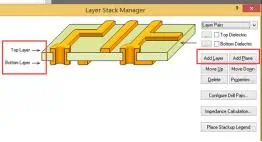
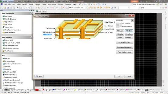
Click Design — Layer Stack Manager in the menu bar, as shown in the figure below:
This is the layer manager. You can easily see the layer distribution in the above figure. This board has only two layers: the top and bottom layers, both of which are signal layers. There are two more options on the right. One is “Add Layer”, the other is “Add plane”. Add layer adds a signal layer, add plane adds an internal electric layer (negative film).
To add a layer, first select a base layer. Then click on “Add Layer” to add the signal layer under the top layer.
Then you can rename the added layer, such as VCC, and add another layer as GND, as shown in the following figure:
Back to the PCB interface, you can see that there are already 4 layers.
You already know how to create 4 layers, 6 layers, even 8 to 20 layers with the same operation.
When dividing the inner electric layer, we can only divide it and could not create a circuit layout, as shown in the following figure:
Adding the internal electrical layer is to add the “add plane” in the Layer Stack Manager.
The internal electrical layer split in the figure above can be split by drawing a line with the place—line command. After the split is completed, double-click to set the network label.
Pay attention to the distribution of components when splitting the internal electrical layer and distribute the same power supply in one area to facilitate the division.
The following is the signal distribution at different layers:
Top layer:
VCC layer:
GND layer:
Since the GND layer is a whole piece of GND, it is sufficient to lay the copper. Pay attention to maintaining the integrity of the GND layer.
Bottom layer:
When open all layers as below shown:
3D drawing:
Main points of 4-layer board wiring:
Pay attention to the distribution of power supply;
Pay attention to the signal line width setting and impedance control;
Distribution of layers, how to arrange 4-layer boards;
4 layer PCB board has GND and POWER layers in the middle of TOP and Bottom layers.
Features of the 4 layer board
1) Reference plane, impedance calculation can be done 2) Shorter return path 3) More layers, simpler design 4) Higher cost than 2-layer board
Based on the wiring density in the layout, look at the densest place of the flying lines, where there are crossovers. It is judged that at least 2 layers of wiring are required, and the cost (design multiple layers regardless of the cost), signal quality consider whether to choose 4-layer board.
After the layout, it is judged how many layers to use, mainly depending on the density of the signal and the place with the most flying lines.
Why Choose to Design 4 Layer PCB
When there is a BGA package, the outer 2 rows can be directly pulled out to go to the top layer. The third and fourth layers can be drilled to go to the bottom layer, and the fifth and sixth rows can be drilled to go to the bottom layer. However, the inside power and ground wirescannot go out, so an additional layer design is required, and two more layers are added.
The power lineblocks the signal line.
Whenline density is not high, you can use a 2-layer board, but you can choose a 4-layer board based on signal quality considerations.
The 4-layer board is laminated based on the double-sided board. When lamination, PP, and copper foil are added on both sides of the double-sided board, it is then pressed into a multilayer board through high temperature and high pressure. In short, the 4-layer board has an inner layer. In terms of the process, some lines will be etched through the inner layer formed by lamination. The double-sided board can be drilled after cutting the raw material sheet directly.
Technology Process difference
Double-sided PCB with HASL surface finished process:
Cutting material grinding → drilling → electroless copper → outer layer circuit → tin plating, etching tin removal → secondary drilling → inspection → printing solder mask → gold-plated → hot air leveling → printing silkscreen → outline processing → testing → inspection
How do you manufacturea 4 layer PCB:
Cutting material and grinding → drilling positioning holes → inner layer circuit → inner layer etching → inspection → black oxide → lamination → drilling → electroless copper → outer layer circuit → tin plating, etching tin removal → secondary drilling → inspection →print solder mask→Gold-plated→Hot air leveling→print silkscreen→routing outline→Test→Inspection
Price difference
PCB production costs are related to the actual area and specific technology requirements. If there are no special requirements, a 4-layer board’s cost is almost 1.8 to 2 times that of a 2-layer board. This is not a linear relationship. If the 4-layer board has impedance or even a blind buried hole design, the price difference is even greater.
Altium Designer 4-layer PCB Design Tutorial
This tutorial allows beginners to get started. The software I use is Altium Designer 13, but the basic operations are similar to other software.
In the PCB interface, click the main menu Design and then click Layer Stack Manager
As shown below:
After clicking, the following layer manager dialog box will pop up. The default is double-panel in AD, so we see only two layers of circuit.
Now let’s add a layer. First, click Top Layer on the left, and then click the Add Plane button in the upper right corner of the layer manager to add an internal electrical layer. Because we are working with a 4-layer board using negative film, you need to add an internal electrical layer and not Add Layer. Afterward, a layer will be automatically added under Top Layer. Double-click the layer, and we can edit the related attributes of this layer, as shown in the figure below:
In the item corresponding to Name, fill in VCC and click OK to close the dialog box. Rename the layer to VCC as the power layer during design. In the same way, add another GND layer. Below is the figure after completion:
3.Import network
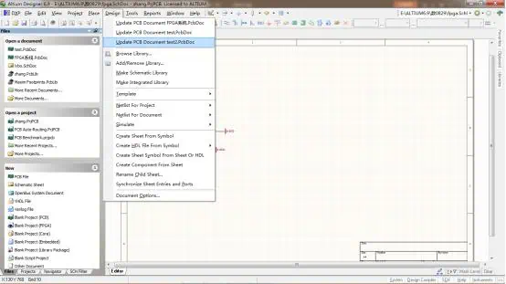
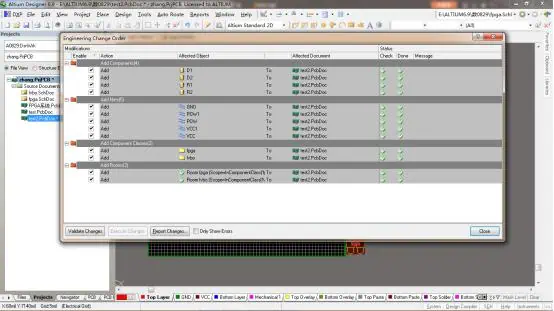
Back to the schematic interface, click the main menu Design ==> Update PCB Document. As shown in the figure:
After finishing the layout of the components on the PCB drawing, draw the outline of the PCB on the Keep Out Layer, as shown below:
Modify the PCB drawing size to overlap the lines of the keep out layer. First, set the grid network width to 20mil. Then click the pad symbol in the shortcut toolbar, and move the mouse to the top left corner of the keep out layer. A circle should appear in the center of the pad. Click the arrow keys on the keyboard to move the pad (click in the left direction, click in the upper direction). Press the enter key, as shown in the figure:
Set the other four corners the same way.
Then click design -> board shape -> move board vertice, overlap the four points on the drawing with the pad placed just on the keep-out line, and click the right button.
Delete the pads on the four corners.
4.Set the inner electric layer; I have divided the inner electric layer in the process here.Then execute design -> layer stack management -> double-click the GND layer, and select the GND network in the NET NAME, which is defined as the GND layer (before, it was just a GND name).
Set the VCC layer: First, enter the VCC layer, use the line place -> line to divide the VCC layer (the closed line or both ends of the line are connected to the outer pullback line), divide into different NET layers, and then click on different areas to select different NET.
At this time, we can see a virtual circle around the pad of the corresponding internal electrical layer. The color of the cross on the pad represents the color of the corresponding internal electrical layer. For example, the inner layer GND is brown, and the cross of the pad is also brown.
p.s
The pullback automatically appears around the PCB drawing after the Layer Stack Manager is set. You can double-click the inner layer to set the pullback line width.
The cross of the pad only appears when the pad is placed on the corresponding net layer. If it is placed on other layers, it will not appear. As long as the cross passes through the VCC layer, it will appear.
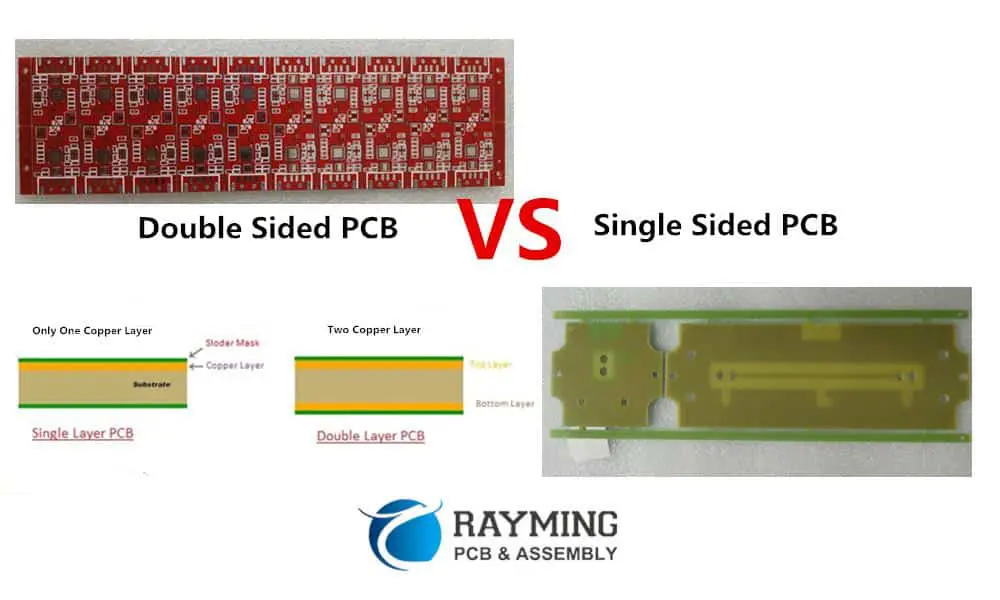
The 2 layer PCB ( double-sided PCB )is a printed circuit board with copper coated on both sides, top and bottom. There is an insulating layer in the middle, which is a commonly used printed circuit board. Both sides can be layout and soldered, which greatly reduces the difficulty of layout, so it is widely used.
To use circuits on both sides, there must be a proper circuit connection between the two sides, as shown in the pictures below. The “bridges” between such circuits are called vias. A via is a small hole on the PCB board filled or coated with metal, which can be connected with the circuits on both sides. Because the area of the double-sided board is twice as large as that of the single-sided board, the double-sided board solves the difficulty of the single-sided board due to the interlaced layout (it can be connected to the other side through the holes), and it is more suitable for more complicated circuits than the single-sided board.
We need electronic products with high performance, small size, and multiple functions, which promotes the development of printed circuit board manufacturing to be light, thin, short, and small. With limited space, more functions can be realized, layout density has become greater, and the hole diameter is smaller. The minimum hole diameter of mechanical drilling capacity has dropped from 0.4mm to 0.2mm or even smaller. The hole diameter of the PTH is getting smaller and smaller. The quality of the PTH (Plated Through Hole) on which the layer-to-layer interconnection depends is directly related to the reliability of the printed circuit board.
The production of double-sided board is more complicated than single-sided board. The main reasons are as follows:
(1) The top and bottom layers of the copper coated board/laminate must be layout
(2) The circuits on the top and bottom layers should be connected with PTH.
Particularly critical among these is the PTH, which is also the core process of double-sided board production. The so-called PTH is created by coating/plating a layer of metal on the inner wall of the via to connect the printed circuits of the top and bottom layers. At present, domestic PTH mainly adopts the electroless copper plating process in China. There are two types of electroless copper plating process:
① The thin copper is electrolessly plated first, then the whole board is electroplated to thicken the copper layer, and finally the pattern transfer is performed.
② The thick copper is electrolessly plated first, and then the pattern is transferred directly.
Both of these processes are widely adopted. However, the electroless copper plating method is harmful to the environment, and it will gradually be replaced by more advanced Black hole technology, tin/palladium direct plating technology, and polymer direct plating technology.
2 Layer PCB With HASL-LF /immersion gold surface production process
Cutting —> Drilling —> Sinking/1ST Copper Plating —> Layout —> Pattern Plating/2nd Copper Plating —> Etching —> Solder Mask —> Legend Printing —>Immersion Tin (or Immersion Gold) —> CNC Routing —> V Cut (some boards do not need this) —> Flying Probe Test —> Vacuum Packaging
Double-sided PCB with gold plating production process
Thin copper —> Thin copper electroplating —> Electroplating thin copper can be replaced by a single process of electroless thick copper plating; both have their advantages and disadvantages.
The pattern plating —> etching method of double-sided board was typical in the 1960s and 1970s. The process of Solder Mask on Bare Copper (SMOBC) gradually developed in the 1980s, and has become the mainstream process especially in precision double-sided board manufacturing.
SMOBC process
The main advantage of SMOBC board is that it solves the short-circuit phenomenon of solder bridging between thin circuits. At the same time, due to the constant ratio of lead and tin, it has better solderability and storage properties than hot melt board.
There are many ways to manufacture SMOBC boards, including the SMOBC process of standard pattern electroplating subtraction and then lead-tin stripping; the subtractive pattern electroplating SMOBC process of using tin plating or immersion tin instead of electroplating lead-tin; the plugging or masking hole SMOBC process; additive method SMOBC technology; etc. The following mainly introduces the SMOBC process and the plugging method SMOBC process flow of the pattern electroplating method and then the lead-tin stripping.
The SMOBC process of pattern plating followed by lead-tin removal is similar to the pattern plating process, and changes only after etching.
Double-sided copper laminate —> According to the pattern electroplating process to the etching process —> Lead and tin removal —> Inspection —> Cleaning —> Solder mask —> Plug nickel plating and gold plating —> Plug sticking tape —> Hot air leveling —> Cleaning —> Legend —> Outline —> Cleaning and drying —> Finished product inspection —> Packaging —> Finished product.
Standard 6 mil trace width is recommended for most designs. Use 4 mil only when necessary for high-density routing (BGA fanout). Narrower traces increase manufacturing cost.
Minimum Spacing
6 mil (Standard)4 mil (Advanced)
Maintain minimum 6 mil spacing between traces, pads, and copper features. For high-voltage isolation, increase spacing according to IPC-2221.
Via Specifications
0.3mm Drill0.2mm Drill
Standard via: 0.3mm drill with 0.6mm pad. Smaller vias (0.2mm) require laser drilling and significantly increase cost.
Annular Ring
5 mil (0.127mm)
The copper remaining around the drilled hole. Larger rings improve yield. For PTH components, use 8-10 mil minimum.
💡
Pro Tip
Designing within standard manufacturing capabilities (6/6 mil, 0.3mm vias, 1.6mm thickness) typically results in 15-30% cost savings compared to advanced specifications.
🎯 Ground Plane Strategy
✅
Recommended Approach
Top Layer: Signal routing + power traces Bottom Layer: Solid ground plane with minimal cuts
Keep ground plane cuts to a minimum
Use ground vias liberally (stitching vias)
Route signals on top layer, crossing perpendicular to minimize coupling
⚡ Power Distribution
Current
Min Width (1oz)
Recommended
0.5 A
10 mil
15-20 mil
1 A
20 mil
30-40 mil
2 A
50 mil
70-100 mil
🔘 Via Placement Guidelines
0.5mm
Via-to-Via Min
0.3mm
Via-to-Pad Min
Place ground vias near signal vias for return current path
Use thermal relief on vias connected to copper pours
Tent vias to prevent solder wicking
🌡️ Thermal Management
Thermal pads: Use large copper pours under heat-generating components
Thermal vias: Array of vias under thermal pads (0.3mm drill, 1mm pitch)
Copper weight: Consider 2oz copper for better heat spreading
🎯
Key Cost Drivers
Board size, quantity, trace/space requirements, via sizes, surface finish, and lead time are the primary factors affecting price.
For prototype quantities, use standard 1.6mm FR-4 with HASL finish and 6/6 mil design rules for the most economical option. Get an instant quote →
❌
Mistake #1: Splitting the Ground Plane
Problem: Routing signals through the ground plane creates slots that interrupt return current paths. Solution: Keep the bottom layer as a continuous ground plane. Route all signals on top layer.
❌
Mistake #2: Undersized Power Traces
Problem: Using 6-10 mil traces for power distribution causes voltage drops and heating. Solution: Calculate trace width based on current. For 1A with 1oz copper: use minimum 20 mil.
❌
Mistake #3: Poor Decoupling Capacitor Placement
Problem: Placing decoupling caps far from IC power pins reduces their effectiveness. Solution: Place 0.1µF ceramic caps within 5mm of each IC power pin.
❌
Mistake #4: Missing Ground Via Near Signal Via
Problem: Signal vias without nearby ground vias create large return current loops. Solution: Place a ground via within 0.5mm of every signal via.
🔍
Pre-Fabrication Checklist
✓ DRC passes with no errors ✓ All nets routed (no airwires) ✓ Gerber files reviewed ✓ Drill file verified ✓ Board outline closed properly
Main process flow of the plugging method
Double-sided copper laminate —> Drilling —> Electroless copper plating —> Electroplating copper on the whole board —> Plugging holes —> Film (positive film) —> Etching —> Removing screen printing materials/Removing plugging material —> Cleaning —> Solder mask —> Plug nickel plating and gold plating —> Plug sticking tape —> Hot air leveling —> The following procedures are the same as above to the finished product.
The steps of this process are relatively simple, and the key is to plug the pores and clean the plugged solder mask.
In the hole plugging process, if the hole plugging solder mask is not used to block the holes and the screen printing imaging, but is replaced by a special masking dry film which is then exposed to make a positive image, this is the masking hole process. Compared with the hole plugging method, it fixes the problem of cleaning the solder mask in the hole, but it has higher requirements for masking the dry film.
The basis of the SMOBC process is to first produce the bare copper double layer board PTH, and then apply hot air leveling.
Pore mechanism
Drill holes on the copper-clad board first. It then undergoes electroless copper plating and electroplating copper to form plated through holes. Both play a crucial role in hole metallization.
The mechanism of electroless copper
In the manufacturing process of double-sided and multi-layer printed boards, it is necessary to metallize the non-conductive bare holes (NPTH), that is, to implement electroless copper to make them a conductor. The electroless copper precipitation solution is a catalytic “oxidation/reduction” reaction system. Under the catalytic action of metal particles such as Ag, Pb, Au, and Cu, copper is deposited.
The mechanism of copper electroplating
The definition of electroplating is to use a power source to push positively charged metal ions in a solution to form a coating on the surface of the cathode conductor. Copper electroplating is an “oxidation/reduction” reaction. The copper metal anode in the solution oxidizes the copper metal on its surface to become copper ions. On the other hand, a reduction reaction occurs on the cathode, and copper ions are deposited as copper metal. Both of them achieve the purpose of perforation through chemical exchange, and the exchange effect directly affects the quality of perforation.
Debris plug holes
In the long-term production control process, we found that when the hole diameter reaches 0.15-0.3mm, the proportion of plug holes increases by 30%.
The plugging problem in the process of perforation
When the printed board is processed, most small holes of 0.15-0.3mm still use the mechanical drilling process. In the long-term inspection, we found that impurities remained in the hole when drilling.
The following are the main reasons for drilling plug holes:
When a plug hole appears in a small hole, due to the small hole’s diameter, it is difficult to remove the impurities inside it by high-pressure water washing and chemical cleaning before copper plating, which prevents the exchange of the chemical solution in the hole during the electroless copper precipitation process and makes the electroless copper lose its effect.
When drilling holes, select suitable drill and backing plates according to the thickness of the laminate, keep the substrate clean, and do not reuse the backing plates. Effective dust collection (using an independent dust collection control system) is a factor that must be considered to solve the plugging hole.
Draw circuit diagram
1. There isa variety of dedicated PCB drawing software, such as Protel, etc., which can draw multilayer (including double-sided) circuit board diagrams. The positions of the layers are aligned, and there are vias to connect the layers.The circuit is connected to realize cross circuiting and facilitate typesetting. After the layout is completed, it can be handed over to a professional board factory to become a circuit board.
2. The double-sided circuit board should be drawn into the circuit schematic diagram in turn, which can be divided into two steps. Step 1: Draw the legends of the main components such as IC on the paper according to the position of the circuit board, arrange and draw the circuit of the pins and the peripheral components appropriately, and complete the sketch. Step 2: Analyze the principle and organize the circuit diagram according to the customary drawing method. You can also use the circuit schematic software to arrange the components and connect them, and then use its automatic typesetting function to organize.
The circuits on both sides of the board should be accurately aligned. You can use the tips of tweezers, the light transmission of a flashlight, and a multimeter to measure the connection and disconnection and determine the connection and direction of the solder and circuits. If necessary, remove the components to observe the layout.
What is the difference between single-sided PCB and 2 layer PCB ?
Single-sided and double-sided boards differ in the number of copper layers. Double-sided has copper on both sides of the board, which can be connected through vias. However, there is only one layer of copper on one-sided board, which can only be used for layout, and the holes made can only be used for SMT.
Single-sided board is the most basic PCB. The parts are concentrated on one side, and the circuits are concentrated on the other side. Because the circuits are only on one side, this kind of PCB is called single-sided. Single-sided boards have many strict restrictions on the design of the circuit (because there is only one side, the circuits cannot cross and must follow separate paths), so only early circuits use this type of board.
There is layout on both sides of a double-sided circuit board, but to use layout on both sides, there must be a proper circuit connection between the two sides. The “bridge” between such circuits is called a via. A via is a small hole filled or coated with metal on the PCB, which can be connected with the layout on both sides. Because the area of the double-sided board is twice as large as that of the single-sided board, it solves the difficulty of the single-sided board due to the staggered layout (it can be passed to the other side through vias), and is suitable for use in more complicated circuits than single-sided board.
Single-sided board: Has copper foil only on one side, such as TV board.
Double-sided board: There are copper traces on both sides, connected by conductive through holes. The price is generally 7 times different (not fully defined due to different materials). There is also a kind of false double-sided board in the industry, which has no through hole connection (much lower cost).
Process
Single-sided PCB board: The solder joints are concentrated on one side, and components are usually inserted on the other side. Some products still have SMD components on the copper-clad side. Double-sided board: Both sides can be layout, and both can have plug-in components or SMD components.
False double-sided PCB: Generally, only one side SMT and layout on the other side. The double-sided copper cladding is connected by circuit on both sides of the component foot.
PCB circuit board
Single-sided board: The metal circuit that provides the connection of the parts is arranged on an insulating substrate material, which is also a support carrier for installing the parts.
Double-sided PCB : When a single-sided circuit is not enough to provide the connection requirements of electronic parts, the circuit can be arranged on both sides of the substrate, and through hole circuits are deployed to connect the circuits on both sides of the board.
2 Layer PCB : AD and CAM CCL cutting/edging —> NC drilling —> PTH —> Pattern plating —> Full plate plating —> Dry film or wet film method masking or plugging holes —> (Negative pattern) (Positive pattern) —> Copper plating/tin lead pattern transfer —> Film removal, etching —> Tin and lead removal, plug plating removal, cleaning —> Printing solder mask/legends —> Hot air leveling or OSP —> Routing/punching shape —> Inspection/testing —> Packaging/finished products.
How do you make 2 layer PCB and precautions
At present, the mainstream circuit board assembly technology in the SMT industry is “full-board reflow soldering (reflow)”. Of course, there are other circuit board soldering methods, and this full-board reflow soldering can be divided into single-sided reflow soldering and double-sided reflow. Single-sided PCB reflow is rarely used now, because double-sided reflow can save space on the circuit board, which means that the PCB can be made smaller. For that reason, most of the boards seen on the market now belong to the double-sided reflow process.
Because the “double-sided PCB reflow process” requires two reflows, there will be some process restrictions. The most common problem is that when the board goes to the second reflow, the parts on one side will be falling due to gravity, especially when the board goes to the reflow zone at high temperatures.
Generally speaking, smaller parts are recommended to be placed on the first side to pass through the reflow oven, because the deformation of the PCB will be smaller on the first pass through the reflow oven, and the precision of solder paste printing will be higher, so it is more suitable to use smaller parts.
Secondly, the smaller parts will not fall off the second time through the reflow oven. Because the parts on the first side will be placed directly on the bottom side of the circuit board, when the board re-enters the reflow zone at high temperature, they are less likely to fall off the board due to excessive weight.
Third, the parts on the first side must go through the reflow oven twice, so their temperature resistance must be able to withstand the heat of the oven twice. The general resistance capacitor is usually required to be able to pass the high temperature at least three times. This meets the requirement that some boards may need to go through the reflow again for repair.
Which SMD parts should be placed on the second side through the reflow furnace? This should be the focus.
Large components or heavier components should be placed on the second side to pass through, to avoid the risk of parts falling into the reflow furnace.
LGA and BGA parts should be placed on the second side through as much as possible, so as to avoid unnecessary remelting risks during the second pass, and to reduce the chance of empty/false soldering. If there are smaller BGA parts, it is recommended to put them on the first side through the reflow furnace.
Placing the BGA on the first or second side through the furnace has always been controversial. Although placement on the second side can avoid the risk of remelting the tin and affecting its quality, the PCB will usually deform more seriously when the second side is passed through the reflow furnace. If the PCB is severely deformed, it can be a big problem for the delicate parts to be placed on the second side, because the solder paste printing position and the amount of solder paste will become inaccurate. Therefore, the focus should be to think of a way to avoid PCB distortion, instead of whether to put BGA on the first or second side.
Parts that cannot withstand overly high temperatures should be placed on the second side through the reflow furnace. This is to prevent parts from being damaged by high temperatures.
PIH/PIP parts should also be placed on the second side to pass through the furnace. Unless the length of the solder pin does not exceed the thickness of the board, the pin protruding from the PCB surface will interfere with the steel plate on the second side, so that the solder paste printed steel plate cannot be flatly attached to the PCB.
Some components may use soldering inside, such as a network cable connector with LED lights. It is necessary to pay attention to the temperature resistance of this part to pass the reflow oven twice. If it fails, it must be placed on the second side.
When parts are placed on the second side, it means that the circuit board has already been baptized by the high temperature of the reflow oven. At this time, the circuit board has become somewhat warped and deformed, which means that the tin quantity and printing position of the paste will become more difficult to control, so it is easy to cause problems such as empty soldering or short circuits. Therefore, it is recommended not to place 0201 and fine-pitch parts on the second side through the furnace. For BGA, try to choose a solder ball with a larger diameter.
In addition, in mass production, there are actually many process methods for soldering and assembling electronic parts on the circuit board, but each process is actually determined at the beginning of the circuit board design, because the placement of the parts will directly affect the soldering sequence and quality of the assembly, and the layout will be indirectly affected.
In order to ensure the reliable conduction effect of the double-sided circuit board, the connection hole on the double-sided board (that is, the PTH) should be soldered with a wire, and the protruding part of the connection wire should be cut off to avoid stabbing the hand. This is in preparation for the wiring of the board.
Devices that require reshaping should be processed according to the requirements of the process drawings:that is, reshaping first and then SMT.
The diode should face up after shaping, and there should be no discrepancyin the length of the two pins.
When inserting devices with polarity requirements, pay attention to ensure that their polarity is notreversed. Roll integrated block components after SMT. No matterwhether they are vertical or horizontal parts, there must be no obvious tilt.
The power of the iron used for soldering must bebetween 25~40W. The temperature of the soldering iron tip should be controlled at about 242℃. If the temperature is too high, the tip is close to useless,and the solder cannot be melted when the temperature is low. The soldering time is controlled at 3~4 seconds.
When soldering, generally follow the soldering principle of the device from short to high and from the inside to the outside. Thecorrectsoldering time must be mastered. If the time is too long, the device, as well as the circuits on the copper clad board, will be burnt.
Because the solderingis double-sided, a process frame for placing the circuit board should also be made, so as not to squeeze the components for the other side.
After the circuit board soldering is completed, a comprehensive check should be carried out to find any missing insertion orsoldering. After quality confirmation, trim the redundant device pins of the circuit board, and then go to the next process.
In anyspecific operation, the relevant process standards should be strictly followed to ensure the soldering quality of the product.
Re-soldering techniques for double-sided circuit boards
When re-soldering a double-sided circuit board, it is difficult to repair because it is dirty, messy, and may have faults such as false soldering, disconnection, and poor contact.
Observation: Based on drawings or prototypes, get a general understanding of the physical layout.
Dismantling: Remove the soldered components, pins andflying leads.
Cleaning: Use absolute alcohol to clean the rosin and soldering on the surface of the circuit board. When cleaning, if you use a soldering iron, it will be faster and the effect will be better.
Layout: Clarify the layout with reference to your observations. If there is no picture, use the drawing method to assist in annotation.
Soldering: Solder according to the clarifiedcircuits. When re-connecting circuit with circuit, try to arrange them on the back.
Inspection: According to the results of the drawing or prototype and the analysis of the layout, check whether the soldering is correct and reliable, and whether the process meets the requirements.
Is so strange for the most of people , is one of Base Material for printed circuit boards. Is low grade in the PCB material industry , Only for Single side PCB, But it is used very widely .
Some People will say Now Technology develop so fast , Every Electronic device become smaller and thinner . Why so low grade material can be use widely .
Is true , Technology is becoming higher and higher , but mean time , Components is also high assemblied more function , This will let more designer use single side PCB ( Cem-1 Material ) to control their Cost .
Single Side PCB ( One Layer PCB ) will reduce the design cost very much , that’s the most important reason .
he materials suitable under the CEM-1 specification in classification of NEMA – the most widespread materials for production of 1-layers printed circuit boards.
Standard CEM-1 material is composite material on a cellulose basis with one layer of glass fibre laminate (FR-4) on a surface. Usually CEM-1 has milky-white color.
The feature of this material is the impossibility of realization the metallization through holes, thus, this material can be used only for production of 1-layer printed-circuit boards.
Standard CEM-1 satisfies to combustibility class UL 94-V0, as FR-4 material. Mechanical characteristics of CEM-1 are little bit worse, than at FR-4: CEM-1 is more fragile. The dielectric constant and a tangent of angle of dielectric losses of both materials are differ insignificantly.
CEM-1 Composite material composed of woven glass fabric surfaces and paper core combined with epoxy resin. Primarily used in the printed circuit board industry. Easy punching and excellent electrical properties and higher flexural strength than paper based grades. CEM-1 provides excellent mechanical and electrical properties, and punches well up to .093″.
CEM-3 is very similar to FR4. Instead of woven glass fabric a ‘flies’ type is used. CEM-3 has a milky white color and is very smooth. It is a complete replacement for FR4 and has a very large market share in Asia. It is a kind of flame retardant epoxy copper-clad plate glass material, is generally used in electronics with double sided and multilayer pcb boards. And CEM – 3 is a new printed circuit substrate material developed based on FR – 4. In recent years, CEM-3 is used to replace FR-4 in Japan, even more than the FR – 4 dosage.
In Next article we will introduce more low grade PCB material for our electronic designer , give a low Cost PCB solution to you .
Fr1 . FR2 , FR3, 22F, CEM 1 ,Cem 3 . FR4, FR5, What’s difference between them ? How to Choose the suitable material for your design? how to control your PCB cost , Let ‘s wait the next article coming .
LED lighting is fast replacing traditional incandescent and fluorescent lighting due to benefits like high energy efficiency, long life and design flexibility. At the heart of an LED lighting product are the LED chips which provide the illumination. Choosing the right LED chips is crucial for achieving the target light output, efficiency, color characteristics and reliability.
This article discusses how to select appropriate LED chips for lighting design including parameters like power, luminous efficacy, color temperature, CRI index and thermal management. Read on for practical guidance to pick optimal LEDs for your lighting application.
Key LED Chip Specifications
The main parameters that characterize an LED chip are:
Power Rating
Measured in Watts
Determines light output
Options range from 0.2W to over 10W
Forward Voltage
Typical values between 2V to 4V
Impacts the driver design
Luminous Efficacy
Measure of light output vs input power
Given in lumens/Watt (lm/W)
Higher is more energy efficient
Peak Wavelength
Determines color – 620-630nm is red, 520-535nm is green etc.
For white LEDs, blue chip + yellow phosphor is common
Color Temperature
Warm white, neutral or cool white
Measured in Kelvin (K)
2700-3000K is warm white, 5000-6000K is cool white
CRI Index
Color Rendering Index
Rating of color quality – maximum of 100
Higher CRI gives better light quality
Viewing Angle
Beam width at 50% intensity points
Narrow (15°), medium (25-50°) or wide (120°+) available
Lifetime
Hours of operation before light output declines by 30%
Higher power LEDs produce greater luminous output. But the increased heat needs thermal management.
For most general lighting like bulbs, downlights and strips, mid-power 1W to 3W LED chips offer a good compromise between light output and easier thermal control vs high power chips.
But specialty lighting like high bay lighting may use higher 5W-10W LEDs. While battery powered flashlights can use tiny 0.2W-0.5W chips.
Lumen Output
The lumen rating of LED chips depends on the power and efficacy. Various luminosity bins are available for each LED chip ranging from low to high lumens.
Typical lumen output for various power LEDs:
1W LED chip – 100 to 130 lumens
3W LED chip – 250 to 300 lumens
5W LED chip – 400 to 500 lumens
10W LED chip – 900 to 1000 lumens
Select chips with lumen output that meet the application’s illumination needs. Combine multiple lower lumen LEDs for higher brightness.
LED Chip Efficacy
Higher efficacy or lumens/watt improves lighting energy efficiency. LED chip efficacy has increased enormously over the years due to technology improvements.
Older LED chips had efficacy of 30-60 lm/W
Mid-power modern LEDs now achieve up to 90-120 lm/W
High power LEDs range from 100-150 lm/W
For a given power rating, choose LED chips with the highest efficacy within budget. This maximizes light output vs power consumption.
Color Temperature
LED Aluminum Substrate
Color temperature determines the visual color tone of white light – from warm white to cool white.
Common white LED color temperatures:
Warm white: 2700K to 3000K
Neutral white: 3500K to 4100K
Cool white: 5000K to 6500K
Warm white is commonly used in homes for cozy lighting. Cool white is preferred where brighter illumination is needed. Select color temperature depending on lighting ambiance needed.
CRI Index
The Color Rendering Index (CRI) indicates how accurately colors are displayed in the light.
Low CRI like 70-75 gives poor color
Medium CRI of 80-90 is generally acceptable
High CRI > 90 approximates natural light
Aim for LED chips delivering 80+ CRI for quality lighting applications. chips with CRI 90+ can provide near natural color rendition.
LED Chip Lifetime
LED chips last much longer than traditional light sources. But over time, light output gradually declines due to phosphor degradation.
30,000 hours is minimum lifetime needed
50,000 hours is typical for quality mid-power LED chips
100,000 hours lifetime LEDs are used for extra reliability
Match the LED chip operating life to the target product lifespan. Also factor in ambient temperature which affects LED lifetime.
Thermal Management
LED chips generate significant heat. Operating at high temperatures lowers light output and shortens lifetime. Effective thermal management is vital.
Use quality aluminum PCBs or ceramic substrates to conduct heat away from the LED chips.
Thermal interface materials like epoxy or grease improve heat transfer to the board.
Ensure ambient air temperature around LEDs stays within recommended range.
Allow spacing between LEDs for airflow to limit temperature rise.
Proper thermal design greatly improves LED chip performance and longevity.
SMD packages allow easier PCB assembly while COB arrays simplify optics design. Consider package height restrictions and soldering processes when selecting.
Conclusion
Choosing optimal LED chips by carefully evaluating key parameters like power rating, luminosity, efficiency, color characteristics, lifetime and thermal management enables creating energy-efficient, long lasting and good quality lighting products. Leverage the latest mid-power and high-power LED chips to realize substantial energy savings and simplified lighting design. With technology advancements delivering ever more performant LED chips, lighting product developers can take advantage by selecting the most appropriate chips to meet their precise application needs.
FAQs
What are the main differences between mid-power and high-power LED chips?
Mid-power LEDs (1-3W) strike a balance between light output and easier thermal management. High-power LEDs (5-10W) produce higher brightness but require substantial heat sinking.
How important is the PCB design for an LED lighting product?
Proper PCB thermal management through large copper planes, thermal vias, airflow and heat sinks is crucial to ensure LED chips operate at optimal temperature for maximum light output and reliability.
What causes LED chips to degrade over their lifetime?
Operating LED chips at high junction temperatures accelerates luminous decay, color shift and failures over time. Quality encapsulation also protects against moisture ingress and corrosion.
Can the color temperature of white LEDs shift over their lifetime?
Yes, white LEDs can gradually shift to a bluer tone over tens of thousands of hours of use. Higher quality LED chips exhibit better color consistency throughout their lifetime.
How does photon efficiency relate to LED efficacy?
Photon or wall-plug efficiency defines the LED chip’s inherent ability to convert electrons to photons. Maximizing this improves luminous efficacy (lumens per watt). Chip design, materials and packaging maximize photon efficiency.