Choosing High Volume PCB Manufacturer

high volume PCB production
high volume pcb manufacturing
High Volume PCB

Find a High Volume PCB Manufacturer and Supplier. Choose Quality High Volume PCB Manufacturers, Suppliers, Exporters at RayPCB.com.Welcome to send your design to Sales@raypcb.com

High Volume PCB Production Manufacturing

1. The RayMing Guarantee

Thinking of PCB Manufacturing with your PCB purchasing? Use RayMing as your go to partner. If there is ever a disruption in your supply chain we have you covered with our manufacturing facility as a backup with competitive prices. So you never have to worry again. Secure your supply chain with RayMing.

RayMing capabilities provide:

Quicker Delivery
Higher Quality
Cost Reduction
Increased flexibility
Seamless facilitation
Supply chain security
Engineering and Technical support
Excellent Customer Service
Account Representation

2. High Lever PCB Equipments to secure your high volume PCB orders

3.Very Strict Quality Control to ensure steady quality PCB delivery

4. 7 x 24 Hours , Customer Services Stand-By

Our high volume PCB manufacturing including Flexible PCB,Led PCB , Rigid-Flex PCB,Rogers PCB and so on, If you have such high volume PCB order, Pls send to quote .

All You Need to Know about High Volume PCB

Circuit boards have become a key cog of every electronic equipment and device in the present-day world. Considering our ever-increasing reliance on electronics for diverse purposes starting from our homes to our workplaces, then the importance of circuit boards will only but increase with time. It is something that I find fascinating considering the evolution of circuit boards from the breadboard days to the new complex, miniaturized printed circuit boards.

Our overreliance on printed circuit boards for our electronic needs calls for a high volume PCB assembly and PCB mass production. Because of this, it not only becomes crucial to undertake high volume PCB production and get an ideal high volume PCB manufacturer to cater to these needs. This article canvasses all the key aspects you need to know about high-volume printed circuit boards. So let us dig in, shall we?

High Volume PCB Production and Assembly

High Volume PCB Assembly

The subject of high volume PCB production and assembly can often prove confusing for both experienced and fresh faces in the circuit board industry. For starters, therefore, it becomes essential to detail what high volume PCB production and assembly refers to and get it out of the way. So what is it all about?

  • High Volume PCB Production

High volume PCB production refers to the last step of the circuit board production process before delivery to customers or clients. It always features no design changes with a linear process that results in large volumes of printed circuit boards. The aim of this process entails producing high volumes of PCBs as required by the client at the least costs, albeit with a high yield rate.

  • High Volume PCB Assembly

High volume PCB assembly implies the assembly of printed circuit boards of ten thousand plus pieces with DFT and DFM. Such a high number requires you to understand what type of PCB you want before engaging a PCB company for your mass PCBย needs. Otherwise, you can end up with large PCB of excellent quality that cannot help your electronic needs. Therefore, the significance of picking the right printed circuit board cannot get understated, especially when it comes to influencing the performance of your electronic product.

What better-printed circuit board manufacturing company to engage for your high volume PCB production and assembly needs than the RayMing PCB and Assembly Company? The company will not only guarantee your mass PCB supply needs through its manufacturing facility but wow you with its printed circuit board capacity in aspects like quick delivery, cost reduction, etc. Additionally, the company possesses high lever printed circuit board equipment to secure your orders, adhere to stringent quality control measures in delivering high-quality printed circuit boards. Whatโ€™s more, the company has a round-the-clock customer support service to ensure a seamless experience during the high volume PCB production and assembly process.   

Maximizing the PCB Production and Assembly Process

In most instances, if not all, maximizing the high volume PCB production and assembly process efficiency often hinges on optimizing the low volume production process. So to maximize the high volume production and assembly process, it becomes imperative to maximize the printed circuit board prototyping phase. So how can you ensure this?

  • Pick a qualified contract manufacturer for your printed circuit board design. The quality of low volume PCB production often hinges on the contract manufacturerโ€™s expertise and equipment in meeting your design needs.
  • Tailor your PCB design to your contract manufacturerโ€™s capabilities. It becomes essential to use specifications that align with the contract manufacturerโ€™s equipment capabilities to ensure timely deliveries, prevent the need for redesigning, and avoid extra development costs.
  • Optimize the selection of your components. A shortage of components often proves a common reason for stalled or disrupted production. It, therefore, becomes pivotal to ensure that all crucial components (of acceptable quality) are available for your anticipated production levels.   
  • Apply decent DFM (design for manufacturing) guidelines. It becomes crucial to assist the low-level production of your printed circuit boards by following design for manufacturing guidelines and rules specific to your contract manufacturer. It will, in turn, help with your high-volume PCB production and assembly process.
  • Perform the required testing of the printed circuit boards. It becomes vital to ensure that every regulatory testing gets conducted on your printed circuit boards post the prototyping stage. However, you should always try and go beyond by performing extra tests to ensure aspects like structural integrity prove sound.

If you optimize the low volume production phase by sticking to the detailed aspects, you will optimize your printed circuit boardsโ€™ high volume production and assembly process. Here, it becomes essential to remember that the initial stages of the production process prove essential as it acts as the basis for the high volume PCB production and assembly.

Easing the Transition from Low Volume/Prototyping to High Volume Printed Circuit Board Production

PCB mass production

You sure understand the importance of PCBs and how the prototyping stage and its optimization impact high volume PCB production. So what happens during the transition process, and how can you seamlessly transition from prototyping to high volume mass production.  

Like in most other real-life situations, the transition from low volume to mass production can prove difficult, though it always comes with incredible gain. In electronics, this prototype-to-mass production transition often proves a significant one. While the base unit remains constant from the prototype level to the high volume production of printed circuit boards, the specific processes often prove unique with particular objectives.

Becoming aware of the differences between the objectives becomes pivotal for engineers and designers of PCBs when picking the ideal contract manufacturer for the two product development phases. Additionally, such knowledge also becomes invaluable in easing the transition from the low volume/prototype phase into the mass or high volume production phase.

Before we delve into the transition process, it becomes necessary to understand what PCB prototyping and high volume production imply. Firstly, the prototyping of PCBs infers the development of small quantities of printed circuit boards that can get deployed for design validation processes by testing the systemโ€™s performance and operation. Therefore, the process must feature aspects such as flexibility, prove sufficiently fast, and get carried out by quality contract manufacturers besides consistent testing. At this stage, any design issues get corrected to avoid any issues on the development of the printed circuit board or post-production in its lifecycle when deployed.    

Conversely, high volume PCB production aims at reliably and efficiently producing high-quality printed circuit boards. The assumption at this stage always encompasses aspects such as the components, design, operation, and functionality having gotten sorted out in the prototyping phase. Because of this, the focus during high volume PCB production revolves around attributes such as reliability, testing, and cost-effectiveness.   

Reliability becomes key because of the large number of printed circuit boards involved that must prove similar in design and quality and at a high yield rate. On the other hand, testing becomes crucial because of ensuring high-quality standards of the PCBs post-production. Finally, the cost aspect becomes crucial because of the large quantity of printed circuit board units. The large number ensures lower costs of production utilizing the principle of economies of scale.

It, therefore, becomes apparent that the objectives between prototyping of PCBs and mass production/high volume production are different.  Consequently, transitioning from one phase to the other will require numerous changes, which include contract manufacturers (when the CM specializes in either of the two). However, it is important to state that if you contact us at RayMing PCB and Assembly, you will not need to change and contract another firm as we cover both aspects.   

The Transition from Prototyping to High Volume Production of Printed Circuit Boards

The transition from the PCB prototyping phase into mass/high volume production must prove seamless and direct in ideal circumstances. However, the transition is never as seamless as everyone would want. Here, you can face countless challenges, such as the need for readjustment of the design files to facilitate quality printed circuit boards. However, the absence of such files can become costly as you will spend more time and money to rectify and produce quality PCBs by having to make engineering design changes.  

Other crucial issues that may arise in the absence of design files include the need to obtain and submit extra design files from your prototype manufacturer to the contract manufacturer. Additionally, your contract manufacturer may lack the capacity to develop your circuit boards in line with similar specifications detailed by your prototype contract manufacturer. It also becomes typical to find components missing even during the PCB production phase. Finally, design changes may become necessary, especially when under performance and operational inadequacies need re-prototyping and redesigning.

Such issues, when they crop up, can delay the high volume PCB production process because of the countless redesign needs you will have to do before the mass production.  While it may not always seem possible to resolve or avert all the potential issues that might crop up, it becomes possible to ease the transition by adopting some crucial PCB product development process guidelines. So how can you ease the transition process from the prototyping phase into the high volume production process?

The best way of ensuring a smooth transition from prototyping into high volume production of printed circuit boards entail finding and picking a contract manufacturer willing to collaborate in creating an excellent final prototype design besides as-built design files to eradicate the need for engineering change order and therefore speed up the high volume production process.

Benefits of Mass/High Volume PCB Assembly

The benefits that accrue from a high volume printed circuit board are numerous and significant.  The benefits include the following.

  • High volume printed circuit board assembly encompasses the need for the prototyping and design functions to get carried out in one go, ensuring that the prototype gets meticulously developed and tested to guarantee accurate functioning. Therefore, it becomes simple to get the large production run going.
  • The high volume PCB assembly ensures mass production of printed circuit board products, something that becomes incredibly useful in going to market at a mass or large-scale level. It ensures large numbers of quality printed circuit board products and quick turnaround periods. Such a situation proves ideal for getting to the market quickly and ahead of the existing competition.
  • Another incredible benefit of high volume printed circuit board production entails the aspect of low production cost. Many cost-related benefits accrue from engaging in a high volume printed circuit board production as high volumes often result in economies of scale. The production cost will impact the pricing of your printed circuit board which enhances your competitive edge in the electronics market. It acts differently from an instance where you produce and assemble small batches, as this always tends to increase the cost.  
  • High-volume printed circuit board production and assembly also provide a shortened production cycle, all thanks to automation. Therefore, it plays a major role in your production pipeline and the go-to-market strategy, which gets a major boost.
  • The mass or high volume production of printed circuit boards also ensures the production consistency and uniformity in features. It results from a scenario that the assembly of each printed circuit board gets a similar assembly and testing regime, which in turn guarantees the quality.

Application Areas of High Volume Printed Circuit Board Assembly Services

  • High-volume printed circuit board assembly services apply in the mass production of electronic appliances.
  • Under typical circumstances, the entry process into new or existing markets in diverse geographical areas requires large-scale printed circuit boards. Because of this, high volume PCB assembly services apply significantly.
  • Mass volumes of PCBs also find application immediately printed circuit boards go beyond the prototype phase of the development, and once every error, if any, gets corrected. It especially becomes essential before the PCBs get to the market. Because of this, it features prominently in the electronic manufacturing sphere, especially for companies where consistency and uniformity prove key.   

Final Thoughts

Printed circuit boards come as an incredibly significant part of electronics, with their manufacturing and assembly become pivotal for every circuit board enthusiast. Because of this, high volume printed circuit board production and assembly become necessary for every person or company interested in designing, engineering, or enthusiast of electronics and circuit boards. So do you want high-volume PCB production or assembly services? Pick RayMing PCB and Assembly today, and you will enjoy it.

Where to order Express PCB

express_pcb

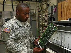
Express PCB Manufacturing Service

RayMing provides hobbyist and engineers from around the world with high-quality Quick Turn PCB at affordable prices. Depending on your PCB requirements, we have a fast turnaround time of just 24 hours. You must submit your files before 9am for same day quick turnaround services. Please call us directly for more information on this service.

Engineers can depend on RayMing because of our reliable on time delivery percentage and high quality manufacturing. Get a faster turnaround time than our standard lead time of 2 weeks, which allows for your company to prototype your critical PCBs faster. With our affordable prices and reliability, decrease the probability for poor quality PCBs and increase your ROI for your PCB prototyping with RayMing .

YouTube video

Submit your PCB specifications by emailing us your Gerber Files , you will attach your gerber files and send them via the mail . Lastly, you can give us a call to talk to a sales representative during normal business hours, or you can click Chat Now to talk with our oversea sales live.

We have many options available for your quick turn PCB manufacturing and with our 10 plus years of fabrication experience, we are confident that we will be able to help you with your project.

When you order from RayMing, you can be sure that your circuit boards will be delivered on time with the highest quality. We appreciate the opportunity to earn your business and we look forward to hearing from you soon.

Quickturn Printed Circuit Board Fabrication Highlights:

Fast turn pcb

Accelerated PCB production times
1 (same day to 24 hours), 2, or 3 day turnaround times
Speed up entry into market
Full and Prototype Boards available
Fast and accurate human reviewed PCB quotes
We provide high quality PCB manufacturing with full in house capabilities for projects small and large.

Over 15 years of Quickturn PCB fabrication supplier experience
State-of-the-Art 18,000 square feet Manufacturing facility
Every received order is manually reviewed before production
No minimum lot requirements on orders
All PCBs manufactured in the our facility

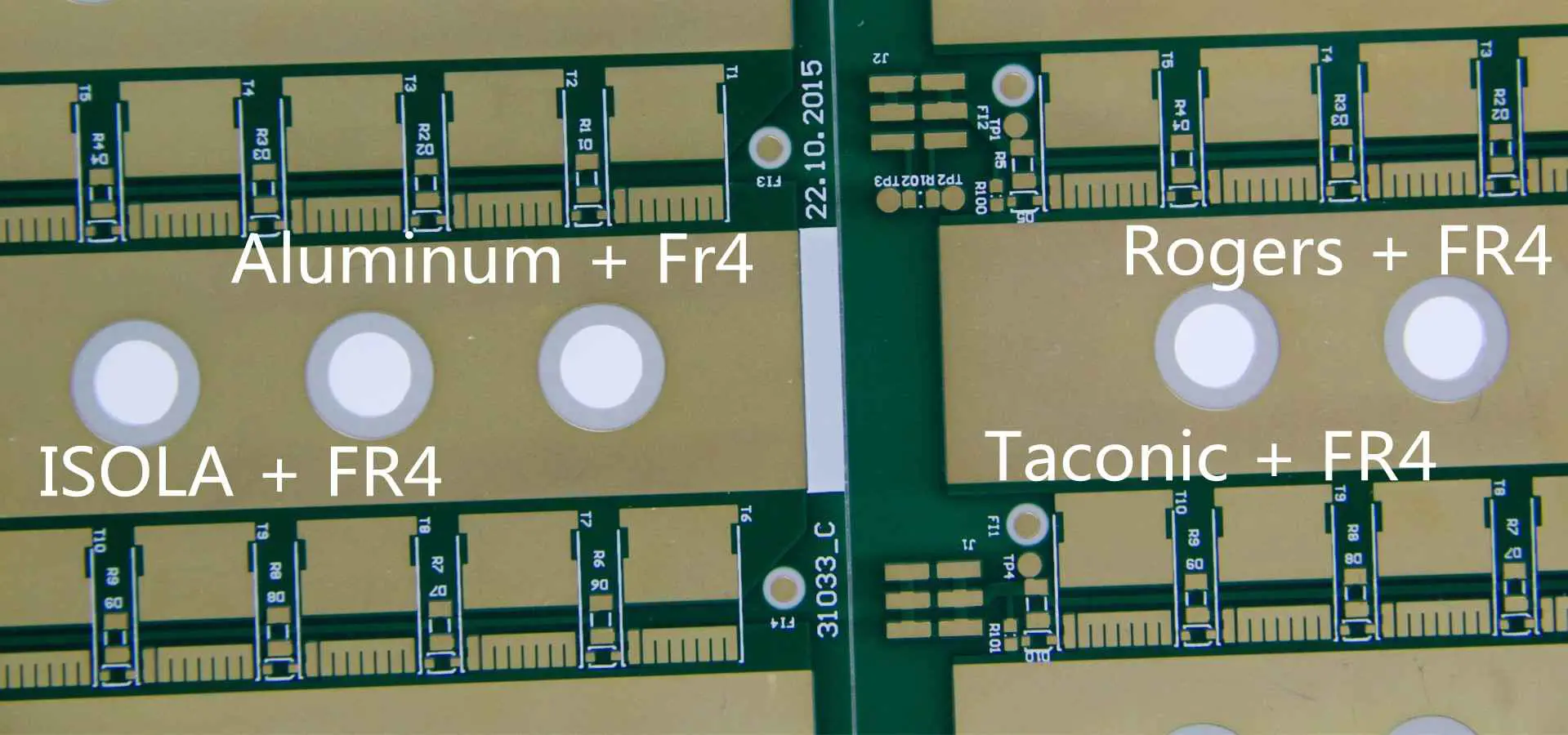
Materials that we keep in stock are:

FR4 (Tg โ€“ 135C, 145C, 170C)
Rogers RO4350
Rogers RO4003
Polyimide
Teflon
Clad Thermal Substrates
Hybrid (Rogers and FR4)
If you donโ€™t see the material above, please contact us because we most likely have it in stock, but not listed above, or can special order it for you.

Finishes we are able to provide our customers:

HASL โ€“ Leaded Solder Tin/Nickel
HASL โ€“ Lead Free Solder
Electroless Soft Gold
Wire Bondable Soft Gold
Nickel Flash Gold
Electroless Nickel
Immersion Gold OSP
Electrolytic Nickel /Hard Gold and Selective Gold
Immersion Silver
Immersion Tin
Carbon Ink
ENIG
Please contact us if you need a finish that is not listed here.

For over 10 years, we have been providing rapid prototyping for our customers, You can send your Quick turn Printed Circuit Board specifications to us. All Gerber files are reviewed in order to provide you with an accurate quote, the first time. We pride ourselves on customer service and our workmanship.

Find a Express PCB Manufacturer and Supplier. Choose Quality Express PCB Manufacturers, Suppliers, Exporters at RayPCB.com.Welcome to send your design to Sales@raypcb.com

How To Get ExpressPCB For Your PCB Design Jobs?

FULL PCB MANUFACTURING Quote

PCB designers are aware of the complexities of designing a printed circuit board and would love to use a feature-rich software. It will reduce the shipment days and complexities by making the design schematics. ExpressPCB is the easiest designing software that you can use to create the boards. This designing software is free to use and supported in Vista, Windows XP, and Windows 7. It is easy to learn, and designers and engineers can use the tool seamlessly. In this article, you can learn how to get ExpressPCB and its unique features.

About ExpressPCB

It is CAD software for creating layouts for printed circuit boards. The CAD is categorized into two sections:

  • ExpressSCH: It is used to create the schematics, and the same design software is incorporated with both Classics and downloads. There is no extra thing to download, and the best part is you do not have to learn anything.
  • ExpressPCB: It is used to design the printed circuit board and linked to the schematic. To Expresspcb.com, the out file is proprietary. For the Gerber files, you have to pay a fee.

The fast PCB tool is used in assembling the components of the basic design, after which you can change the design quickly. First, the changes are done into the schematics drawing and then into the PCB design layout. The multi-rich software is flexible and can efficiently attain the demands of desired projects.

Check out The Process To Get ExpressPCB

The Downloading Process: When downloading the software, you can get it easily from expresspcb.com. The latest versions are present on the website and use the one according to your desires.

Start Using The Software: You must follow the step-by-step procedure to design the PCB using the tool.

  1. Open the tool, and a dialog box will appear with two links. It would be best if you went through both the links as they contain instructive information. After that, press the “OK” button to start the file.
  2. Here you must select a new file, following which a dialog box will open up. The next thing to do is you have to set the dimensions. By default, the dimensions would be 0.056 round with 0.029 holes. It is the maximum default size but can be changed according to your needs.
  3. Now place all the components in the place and click on the IC icon present in the toolbar. Pull down the menu to pick the necessary components and double click on them to get the properties.
  4. Click on the same icon if you need a transistor and place it on the Dip-8 pin. After that, for the capacitor, write the cap and assign the part IDs and names.
  5. If none of the components are present, you have to follow the same procedure for all. You have the flexibility to draw on your own.
  6. Before proceeding to the component and picking the ungroup PCB, select similar components.
  7. Draw a circle for photo-resistor and set the radius and width of the line,
  8. Click on the whole part and proceed to the component. Pick on the group to create the PCB components.
  9. After that, assign the unique ID and name as you can double-click components and set the parameters.
  10. Save it as custom components which will help you to use it again if needed.
  11. You must repeat this step for the entire procedure while making parts.
  12. For placing power and the grounds into the circuit, pick on the “Filled Planes” bar. It is present on the toolbar, and then you must select on it to press the layer.
  13. Draw a horizontal line, and you must drag it squarely and pick the place traces.
  14. While doing so, you will find that an isolated path is formed, separating the ground from power.
  15. Go to the bottom right corner and then to the left corner and right-click at the box end.
  16. As the filled plane gets added to the circuit, you must change the plan shape.
  17. Using solid or thermal shape, you must connect the pads.
  18. By right-clicking on the right-pad, you should connect the plan. Following this, you can pick the type of plane and pad. With this, you will have a thermal/solid plane and pad.
  19. In the design, there can be an area where you do not find a filled plan. Here you must select this option and pick the area keeping the plane away from the top toolbox.
  20. In this way, you can keep the area out of the filled plane.
  21. Similarly, draw a square in the same area where you do not need a filled plane. Here the area will have the dotted lines.
  22. Follow this step for all the pads, and while doing, you can see the layout on the screen.
  23. By using the fast turn PCB software, you can design several layers.
  24. Firstly, you must set the number of copper layers and then click on them in the layout menu.
  25. If you choose the four layers, it will add two inner layers, where the first is the ground plane. The next one is the power plane, and both layers are of copper. It helps in improving the noise immunity of the circuit.
  26. After completing the layout, the software will tell the price you need to play to get the boards.
  27. Take a print of the manufacturing printed circuit boards. A few precautions are there to keep in mind when taking the print. If you do not, there can be high failure chances in the layout. The precautions to keep in mind are:
  28. Ensure the tracks should not have less than 100 degrees bends.
  29. The device might fail if the way touches each other, so make sure that it does not happen.
  30. After preparing the entire fast PCB prototyping, you can move, delete, copy and even rotate the component.

Place An Order: Now that you have completed the design of the printed circuit board, go ahead and place an order. Here are the steps you must follow now.

  • Run the program, which means the ExpressPCB on the laptop or desktop, and get the file.
  • Before submitting, you can ask for an exact estimate to get the board through the Compute board cost command. It is present on the layout menu.
  • Click on the button that says “Order Boards Via The Internet” and place the order. Before doing this, make sure the PCB file is loaded.
  • A form is there where you have to fill in the particulars like name, email address, and address. Click on the manufacturing option that you want, like Standard, 4 Layer-Production, Production, etc.
  • Enter the number of boards you need, as it will help specify the exact amount to get them.
  • Now you have to make the payment using credit cards as they use only this form of payment.
  • Before playing the 24 hour PCB board, you have a chance to review the entire thing and the cost. If you want to make any changes, this is the time to do so.
  • Once you are ready to submit, click on the “Send” button. After this step, you will get a mail confirming the details on the email address within an hour.
  • You have to wait for some time and then get the printed circuit board.

Features Of ExpressPCB Software

Rogers RT duroid 6035HTC PCB

Quite a few features are there about the multi-functional PCB express software. Out of which, some features are here which you can go through once:

  • Easy To Use: Most importantly, the software is simple and easy to use. By pressing on the drop-down menu, you will come across all the components and signs. Then double-click on them to use whichever is required. It simplifies the design’s complexities. It has industry-recognized notations, like dimensions, schematics, and designers can use multi-layer or single-layer boards.  
  • Allowing To Copy And Paste: The software will enable you to copy and paste multiple times to get the desired product. Till the last step, you have the freedom to make changes and eliminate big errors. The software has easy-to-use interfaces that reduce production time as well.
  • Streamline The PCB Ordering Process: It is a fast and reliable software you can get the next day PCB. You can use the tool for free and streamline the ordering process. There are advanced component search and component search builders that make the entire process much easier.
  • Ability To Modify: By using the tool, you can modify the printed circuit board layout. It has free-form and parametric editing tools and an asymmetrical editing process. You can create custom commands and change the customization file.

Final Thoughts

Well, by using ExpressPCB, engineers and designers can shorten the time to market the new products. In addition, they can pick and test electronic components in a 3D environment. The software helps reduce the production cost to a great extent that you would have spent designing the prototypes. It is said that this process is optimal and most cost-efficient to create the final product. In that way, the errors can also be reduced automatically.

Taconic PCB Manufacturer

Taconic PCB

Taconic PCB Manufacturing services

Taconic PCB
Taconic PCB

Taconic PCB A leader in the development and manufacture of advanced engineered composite materials. By pioneering the manufacture of PTFE coated fabrics and other high-temperature/non-stick materials, Taconic has become a leading supplier to the food processing industry. They also supply a wide range of coated materials, including tapes, fabrics and belts for a wide variety of industrial applications.

The companyโ€™s Advanced Dielectric Division supplies high-quality circuit board materials to the fast growing wireless communications industry. Today, Taconicโ€™s commitment to customer service and the production of high-quality, reliable materials as well as its ability to keep pace with changing industry needs distinguish it as a leader in materials supply.

Microwave and RF PCB applications need laminates with electrical, thermal, mechanical, or performance characteristics that exceed standard FR-4 materials.Taconic , Arlon,Teflon,Rogers PCB, Nelco PCB Material all belong to Mircrowave/RF PCB Material .

Printed circuit boards are without doubt an integral part of electronics production. Over the years, these boards have continued to meet various demands of engineers. Taconic PCBs are one such PCB. These PCBs have various benefits and features that make them distinct.

Taconic laminates are utilized for high-performance and high-frequency applications. Taconic is committed to meeting the demands of the marketplace across the globe. It achieves this by providing high-frequency PTFE laminate materials.

Taconic PCB: What Does This Mean?

Taconic RF-35A2 Ultra pcb

Taconic PCB is a printed circuit board fabricated with the use of Taconic PCB materials. These materials are Ceramic-filled Polytetrafluoroethylene and woven glass reinforced materials. These boards are suitable for RF applications in the communication and aerospace industries.

This printed circuit board features low dielectric loss and electrical signal loss which makes them an ideal option for several applications. This circuit board was designed to meet the rising demands of the electronic world. Taconic PCBs feature a wide range of dielectric constant values.

Taconic is a well-known brand in radio frequency laminates. It provides printed circuit boards that are utilized in the fabrication of high-performance digital boards, multilayer RF, and other electronic devices. Taconic laminates can be milled, plated, and sheared using standard methods.

RayMing 2 Layer Taconic TLY-5 PCB 0.508mm Thickness

RayMing 2 Layer Taconic TLY-5 PCB 0.508mm Thickness

Original price was: $1,460.00.Current price is: $1,420.00.

Taconic TLY-5 PCB 2 layer Surface finish: Immersion Gold Board Thickness: 0.508mm Solder Mask: Green Size: 100x100mm Quantity: 10pcs   Taconic tly-5 datasheet :ย  AGC_TLY-5_TDS   What is Taconic TLY-5 ? Taconic TLY-5 is a type of printed circuit board (PCB) material. It is a woven fiberglass fabric pre-impregnated with a polytetrafluoroethylene (PTFE) resin system.…

Category:
Tags:

What is the difference between Taconic PCB and Isola PCB?

Many people have wondered what the difference between Taconic and Isola PCB is. These two printed circuit boards have similar benefits but are different from each other. Taconic PCB utilizes ceramic-filled Polytetrafluoroethylene or reinforced glass Polytetrafluoroethylene PCB which makes it thermally and electrically stable.

Taconic boards incorporate thermoplastic prepregs and thermoset to meet the demands of high-performance boards. These circuit boards are ideal for microwave or radio frequency designs.

Meanwhile, Isola PCB utilizes copper-clad laminates and dielectric prepregs for its fabrication. These laminates have resin compositions to meet the demands of high-performance applications. Isola PCB features great mechanical, thermal, and electrical properties. These properties are more than what FR-4 materials offer.

Taconic and Isola PCBs are specifically designed for high speed and high-performance applications, but these boards utilize different materials in their production.  

Benefits of Taconic PCB

Low cost: When it comes to the fabrication of this circuit board, low cost is required. It is always a budget-friendly option for engineers. This ceramic-filled laminate offers the best value for its price.

Low dielectric loss: Low dielectric loss laminates are an ideal option in radio frequency and microwave applications. Taconic features a very low dielectric loss. The low dielectric loss of this material is a result of the dielectric constant of this material.

Low electrical signal loss: This is one of the great benefits of these boards. Taconic laminate offers low dielectric signal loss due to the material used in its fabrication.

Wide range of dielectric constants: Taconic PCB offers a wide range of dielectric constants. This makes it ideal for use in various applications.

Low dissipation factor: This circuit board features a low dissipation factor, which makes it a good insulating material. A low dissipation factor indicates an efficient insulator system.

Great dimensional stability: Taconic PCB maintains its original dimension even when subjected to heat. Engineers use this circuit board for applications that are likely to be exposed to varying temperatures.

Low moisture absorption: This board features a low rate of moisture absorption. Therefore, it can be used in humid environments. Moisture is harmful to PCBsโ€™ durability, so, a PCB that absorbs low moisture is an ideal option.

Factors to consider in Hybrid Fabrication of Taconic PCB

Some factors need to be considered during the hybrid fabrication of Taconic PCB i.e. Taconic rf 35 pcb.

Drill parameters: Drill parameters is a key factor to consider since it determines proper hole formation. The feeds and speeds of the drill are determined by the stack-up materials. During hybrid fabrication, the speeds and feeds need to be adjusted. For example, some components dispense much heat and this can lead to deformation.

Compatible materials: Materials utilized in the hybrid stack-up should match with the lamination cycle. Some materials need higher temperatures and pressures during the lamination procedure. You should always check the datasheets of the material to confirm the use of the materials before using them for design.

Preparation of hole wall: After the hole has been drilled, then the preparation of the hole wall is the next thing. For each general group, there may be process instructions. You must refine the process per material to achieve total reliability.

Types of Lamination Methods in the Manufacturing of Multilayer Taconic PCB

In the manufacturing of Taconic PCB, several types of lamination procedures are utilized. These methods are very vital as they ensure Taconic PCBs go through the right production process.

Multilayer PCBs: Multilayer PCBs have several layers. These can be thin etched boards or trace layers. Bonding is achieved via lamination. The internal PCB layers get exposed to very high temperatures and pressure during the process of lamination.

Double sided PCBs:  Double sided circuit boards may be different from some PCBs, but the process of lamination is the same. For the lamination of the PCB panel, engineers use a layer of photosensitive dry resist.

PTFE microwave laminates: These laminates are one of the most common laminates used for PCB lamination. PTFE microwave laminates feature uniform dielectric constant, low electrical loss, and thickness tolerance. These laminates are considered an ideal option for radiofrequency PCB applications.

Sequential lamination: This type of lamination method is used if the circuit board has two or more subsets. In this method, multiple layer subsets are combined in various procedures.

Types of Taconic Laminates

Taconic RF-60TC PCB

Taconic offers several high-frequency laminates. Each of these laminates features outstanding properties and benefits. Let us have a look at the types of Taconic laminates available

Taconic rf 35

This is a type of laminate offered by Taconic. This laminate is ceramic-filled and reinforced with woven glass. It is ideal for high-performance applications like antennas, power amplifiers, and passive components.

This laminate is the perfect solution for RF and microwave applications. It features properties like low dissipation factor, low moisture absorption, and great dimensional stability. Taconic rf 35 pcb is RoHS compliant. This laminate is compatible with several hybrid builds.

Engineers combine Taconic RF-35 with hybrid multiple layer boards. The combination of these high-grade materials will help to enhance reliability.

Taconic CER 10

This is another great laminate offered by Taconic. It is a ceramic-filled laminate reinforced with woven glass. Taconic CER 10 features solder resistance and uniform electrical properties. This laminate is used in several applications like couplers, power amplifiers, filters, and passive components.

Taconic CER 10 has an interlaminar board and it is clad on one or both sides. This dimensionally stable laminate is an ideal option for high volume and low-cost applications. This laminate goes through a flammability test. Taconic CER 10 is clad with Brass, aluminum, or copper.

This laminate provides great thermal and mechanical properties. It is also ideal for microwave designs. Taconic CER 10 has flexural strength and low moisture absorption.

Taconic tly-5

Taconic tly-5 is manufactured by Taconic. These laminates have dimensional stability and uniform dielectric constant. Their dielectric constant is measured at 2.20 and .0050 is their dielectric thickness. Taconic tly-5 is used in applications such as power amplifiers, aerospace, cellular communications, automotive radars, and satellite communications.

Materials such as aluminum, copper, and brass are used to clad this laminate. Thus laminate is reinforced with woven glass. It is often used for low-cost applications that require high performance. This dimensionally stable material goes through a flammability test.

Taconic tly-5A

Taconic tly-5A is a dimensionally stable and high-frequency laminate. This laminate offers the lowest dissipation factor among the Taconic laminates. PTFE is the material used for coating this laminate. It is also reinforced with woven glass like other Taconic laminates.

This laminate can be used in several applications like aerospace, power amplifiers, satellite communications, and the automotive radar industry. This laminate features low water absorption and high peel strength. It also features a low dielectric constant. Taconic tly-5A can be used with hybrid builds.

Frequently Asked Questions

Does moisture affect Taconic PCB performance? Moisture can influence PCB performance since its water content to moisture absorption can affect loss performance. Taconic PCB materials have high dielectric constant water which is about 70. Most times, laminates fabricated for high-performance applications have low moisture absorption with values lower than 0.2 % or 0.2%.

How can I reduce PCB insertion loss? You can reduce the insertion loss of PCB by utilizing broader traces, minimizing the DK of the PCB, integrating thicker dielectrics, and making sure looser coupling occurs.

Conclusion

Taconic offers high-frequency PCBs ideal for different applications. Taconic PCBs have a wide range of dielectric constant, low dissipation factor, and low electrical signal loss. These laminates are reinforced with woven glass. They have great thermal, mechanical, and electrical properties.

Taconic substrate PCBs are available in different types. These printed circuit boards are fabricated with a myriad of materials that guarantee high reliability. These materials are used for applications like aerospace, automotive radar, and power amplifiers. Taconic is a well-known brand that has continued to maintain a long-standing reputation in the PCB industry.

Fast Turn PCB Prototype service your design Verification

Megtron 6 pcb

What is PCB prototype service

PCB prototype service is a specialized offering that allows engineers, designers, and hobbyists to create a small batch of printed circuit boards (PCBs) for testing and validation before moving to full-scale production. This service is essential for verifying the design, functionality, and performance of a PCB in real-world conditions.

Key features of a PCB prototype service typically include:

  1. Rapid Turnaround: Quick production times, often as fast as 24 hours, to accelerate the development process.
  2. Customization: Support for various PCB types, such as single-layer, double-layer, multi-layer, HDI, rigid, flex, and rigid-flex boards.
  3. Advanced Technologies: Capabilities like impedance control, blind/buried vias, micro-vias, and high-frequency materials for specialized applications.
  4. Quality Assurance: Testing and inspection to ensure the prototype meets design specifications and functional requirements.
  5. Cost-Effectiveness: Affordable pricing for small batches, reducing upfront costs during the design validation phase.

PCB prototype services are critical for identifying and resolving design flaws early, saving time and money in the long run while ensuring the final product performs as intended.

What Does RayMing Offer for fast PCB Prototyping?

PCB prototyping used to be a daunting challenge for many electronics professionals. RayMing now puts an end to those struggles! We can deliver your first-run boards correctly in just 24 hours!

The prototyping phase is the most crucial stage for engineers, students, and hobbyists. At RayMing, we not only deliver your boards quickly but also ensure precision, quality, and cost-effectiveness. This significantly reduces your expenses and accelerates the development timeline for your electronic products.

Our PCB portfolio spans a wide range of products, from simple 2-layer boards to highly advanced HDI and flexible circuits. Despite the diverse functionalities and applications of the PCBs we produce, they all share one common factor: our team of experts meticulously oversees every step of productionโ€”from prototyping to volume manufacturingโ€”ensuring adherence to our rigorous processes and product specifications.

Multilayer PCB Prototype
Flex PCB Prototype
Rigid Flex PCB Prototype
Rogers PCB Prototype
Ceramic PCB Prototype
Aluminum PCB Prototype
HDI PCB Prototype
RF PCB Prototype
Heavy Copper PCB Prototype

Custom PCB Prototypes for Any Product

We specialize in creating custom prototype printed circuit boards tailored to your specific needs, whether for barebones testing or complex designs. Our prototype PCB fabrication services are designed to handle both simple and highly intricate projects, accommodating any layer count, materials, densities, processes, and finishes your project demands.

If youโ€™re looking for a quick-turn prototype PCB manufacturer that is collaborative, reliable, and cost-effective, RayMing PCB is your ideal partner. We are committed to delivering high-quality prototypes that meet your exact requirements, ensuring your product development process is smooth and efficient.

We also provide one-stop solution for your PCB prototype, Click to Check our prototype PCB assembly service .

Professional PCB Clone and PCB Copy Services – Expert Circuit Board Duplication

Are you looking for reliable PCB clone and PCB copy services? When you have a physical electronic circuit board but lack the original design files, our professional PCB clone service provides the perfect solution. Whether you need PCB copy for obsolete boards or circuit duplication for production scaling, we deliver precision results.

YouTube video

What is PCB Clone and PCB Copy Technology?

PCB clone, also known as PCB copy or PCB duplication, is an advanced reverse engineering technology that creates exact replicas of existing printed circuit boards. Our PCB clone process analyzes your original board and produces identical copies without requiring original design files or Gerber drawings.

Key Features of Our PCB Clone Service:

  • Complete PCB copy from physical samples
  • Schematic diagram restoration
  • Bill of Materials (BOM) generation
  • Gerber file creation
  • Component identification and sourcing

Why Choose PCB Clone Over Traditional Design?

Cost-Effective PCB Copy Solutions

Traditional PCB design from scratch involves significant costs including prototype development, testing, and design optimization. Our PCB clone service eliminates these expenses by reverse-engineering existing boards. PCB copy technology reduces development time and costs by up to 70% compared to original design processes.

Fast Turnaround PCB Clone Process

Our streamlined PCB clone workflow ensures rapid delivery:

  1. Sample Analysis: Send photos of your board for initial PCB copy assessment
  2. Quotation: Receive detailed pricing for your PCB clone project
  3. Sample Submission: Ship physical samples for precise PCB copy analysis
  4. Reverse Engineering: Our experts perform comprehensive PCB clone procedures
  5. Deliverables: Receive complete files including Gerber, schematics, and BOM

Professional PCB Copy Applications

Legacy System Replacement

When original manufacturers discontinue support, PCB clone services become essential. Our PCB copy expertise helps maintain critical systems in:

  • Industrial automation equipment
  • Medical devices
  • Aerospace applications
  • Telecommunications infrastructure

Production Scaling Through PCB Clone

Manufacturers use PCB copy services to scale production without licensing fees. Our PCB clone process enables:

  • Rapid prototyping
  • Cost reduction
  • Supply chain independence
  • Quality improvement opportunities

Advanced PCB Clone Techniques

Multi-Layer PCB Copy Capabilities

Our PCB clone service handles complex multi-layer boards with precision. Advanced PCB copy techniques include:

  • Layer-by-layer analysis
  • Via mapping and reconstruction
  • Trace routing optimization
  • Component placement accuracy

Intelligent Component Analysis

Modern PCB clone projects often involve microcontrollers and programmable devices. Our PCB copy service includes:

  • Firmware extraction (where legally permissible)
  • IC programming analysis
  • Memory dumping procedures
  • Code reverse engineering

Quality Assurance in PCB Clone Projects

Precision PCB Copy Standards

Every PCB clone project undergoes rigorous quality control:

  • Dimensional accuracy verification
  • Electrical continuity testing
  • Component value confirmation
  • Performance validation

Testing and Validation

Our PCB copy process includes comprehensive testing:

  • Functional verification
  • Signal integrity analysis
  • Thermal performance assessment
  • Reliability testing

Industries Served by PCB Clone Services

Automotive PCB Copy

The automotive industry relies on PCB clone services for:

  • ECU replacement modules
  • Legacy vehicle support
  • Performance modifications
  • Cost optimization

Medical Device PCB Clone

Healthcare equipment manufacturers use PCB copy for:

  • Life-critical system maintenance
  • Regulatory compliance
  • Obsolescence management
  • Cost-effective repairs

Consumer Electronics PCB Copy

Consumer product manufacturers leverage PCB clone for:

  • Product improvement
  • Cost reduction
  • Feature enhancement
  • Market adaptation

Technical Specifications for PCB Clone Projects

PCB Copy Capabilities

  • Board thickness: 0.2mm – 6.0mm
  • Layer count: 1-30 layers
  • Minimum trace width: 0.075mm
  • Component density: High-density support
  • Material types: FR4, Rogers, polyimide, aluminum

PCB Clone Accuracy Standards

  • Dimensional tolerance: ยฑ0.05mm
  • Component placement accuracy: ยฑ0.025mm
  • Electrical performance: 100% functional equivalence
  • Material matching: Exact or equivalent specifications

Getting Started with PCB Clone Services

PCB Copy Consultation Process

  1. Initial Assessment: Submit clear photos of your PCB for preliminary PCB clone evaluation
  2. Technical Review: Our engineers analyze complexity and provide PCB copy recommendations
  3. Proposal: Detailed quotation including timeline and deliverables
  4. Sample Analysis: Physical board examination for precise PCB clone specifications
  5. Project Execution: Professional PCB copy implementation with regular updates

PCB Clone Documentation Package

Every completed PCB copy project includes:

  • Complete Gerber file set
  • Drill files and NC data
  • Pick and place files
  • Bill of Materials (BOM)
  • Assembly drawings
  • Test procedures

Cost Factors in PCB Clone Projects

PCB Copy Pricing Considerations

PCB clone costs depend on several factors:

  • Board complexity (layer count, component density)
  • Component identification requirements
  • Firmware analysis needs
  • Documentation depth
  • Quantity requirements

Value Proposition of PCB Clone

Compared to original design, PCB copy services offer:

  • 60-80% cost reduction
  • 70% faster time-to-market
  • Reduced risk through proven designs
  • Immediate availability

Advanced PCB Clone Technologies

pcb reverse engineering tutorial

High-Frequency PCB Copy

Specialized PCB clone techniques for RF and microwave applications:

  • Impedance matching preservation
  • Signal integrity maintenance
  • Material property analysis
  • Performance optimization

Flexible PCB Clone Services

Our PCB copy capabilities extend to flexible circuits:

  • Flex-rigid board analysis
  • Bend radius optimization
  • Connection reliability
  • Dynamic application support

Quality Management in PCB Clone

ISO Standards Compliance

Our PCB clone processes follow international standards:

  • ISO 9001:2015 quality management
  • IPC standards compliance
  • RoHS and REACH compliance
  • Industry-specific certifications

Continuous Improvement

We enhance our PCB copy methodologies through:

  • Technology upgrades
  • Process optimization
  • Customer feedback integration
  • Industry best practices adoption

Intellectual Property Considerations

pcb reverse engineering software

Ethical PCB Clone Practices

Our PCB copy services operate within legal frameworks:

  • Customer ownership verification
  • Reverse engineering legality
  • Confidentiality agreements
  • Ethical business practices

Protecting Your PCB Clone Investment

We safeguard your PCB copy projects through:

  • Secure data handling
  • Non-disclosure agreements
  • Proprietary information protection
  • Long-term support commitments

Contact Us for PCB Clone Services

Ready to start your PCB clone or PCB copy project? Our expert team provides comprehensive circuit board duplication services with guaranteed quality and fast delivery. Contact us today for a free consultation and discover how our PCB clone expertise can solve your electronic design challenges.

Email: sales@raypcb.com Services: Complete PCB clone and PCB copy solutions Specialties: Multi-layer boards, high-frequency circuits, legacy system replacement

Transform your electronic projects with professional PCB clone and PCB copy services that deliver precision, reliability, and cost-effectiveness.

Military & Defense PCB, Military Component Supplier

Defense PCB
what is pcb assmebler

Military Grade PCB

Project Detail:

Material๏ผšFR4+Rogers 4350B

10 Layer 1.6mm PCB

Line width/space:4mil/mil

Min hole:0.2mm

Military is one sectors that is highly demanding when it comes to their applications. The systems or devices that are used in these sectors have to be of superior quality. The printed circuit boards developed at RayPCB fulfill such quality requirements and thus they are chosen for various applications pertaining to the military sector.

Military Grade PCB require high reliability with long service times under extreme conditions. We produce military PCBs for aviation, ground activities, defense, naval applications, and space weapons. RayMing provides printed circuit boards that offer a wide range of materials, composites, and construction, that are very effective in military applications.

High temperature laminates, copper and aluminum substrates can perform very well in these challenging environments. Anodized aluminum can be utilized to eliminate the effects heat induced oxidation. Aluminum substrates combined with thermally conductive pre-pregs gives the military designer performance with weight advantages.

military PCB circuit board
Military PCB Circuit Board

The following represents a few military applications:
Over horizon enforcement networks (Cyber counterintelligence systems)
Cross targeting systems (Cryptanalysis systems)
Automation networks (Command and control systems)
Air cartographic photography (Automatic search jamming systems)
Radio communication systems (AMRAAM โ€“ Advanced Medium Range Air to Air Missiles)
Radar installations (APU โ€“ Auxiliary Power Units)
Power converters (ASRAAM โ€“ Advanced Short Range Air to Air Missiles)
Power supplies (AWACS โ€“ Airborne Warning and Control System)
LED lighting systems (AEW&C โ€“ Airborne Early Warning & Control)
Instrumentation (CIWS โ€“ Close In Weapons Systems)
Control tower systems (ECCM โ€“ Electronic Counter-Countermeasures)
Temperature sensors (FLIR โ€“ Forward Looking Infrared)
Audio interface applications (IADS โ€“ Integrated Air Defense System)

All about the Design Rules and Specifications for Military PCB Manufacturing

military rogers pcb

Printed circuit boards have diverse applications owing to their significance in electronics. Key among the application areas include the military sector. However, you may know very little about military-grade PCB due to the nature and sensitivity of this unique sector. So what does it all entail? This article aims at answering all the potential areas of significance you may want to understand about military manufacturing and the military PCB. This is the only article about military-grade capacitors which provides an overview of the PCB industry for military use. It reveals how military prototypes and PCBs have been designed and manufactured with the special requirements that this industry demands. This is a necessary read for anyone interested in designing, manufacturing, or servicing PCBs manufactured for defense applications.

Military-grade components require a very high degree of quality control and rigorous tolerances, which may not be possible to achieve using conventional manufacturing methods. The military PCB industry has evolved to produce components and boards for demanding applications. This section describes state of the art in military PCB manufacturing. In addition to discussing the basics of PCB manufacture, we will also discuss factory layout and design considerations.

The Military PCB

Military applications need printed circuit boards. However, the harsh environment that characterizes the military requires a highly reliable PCB. The typically printed circuit board is unheard of to work in an environment with constant contact and interaction with contaminants, extreme temperatures, and chemicals without problems. It is where the military printed circuit board comes to play.

The military PCB has to meet or exceed the requirements and specifications set by the respective military. Because of this, such printed circuit boards are of diverse types based on the requirements and the specific application area specified by the military. Consequently, the type of military PCB will determine the board specifications. Additionally, you have to consider specific design features from conceptualization all through the manufacturing process.

Additionally, getting the right military PCB manufacturer becomes important. The company will source the materials and components desired for the military PCB design and fabricate and mass-produce the PCB according to your needs. Remember, military-grade PCBs require a high level of quality and reliability, and picking a top manufacturer starts the process.   

What better entity to cater to your PCB military manufacturing needs than us at RayMing PCB and Assembly? The company guarantees top-quality military printed circuit boards, including aviation, defense, space, ground activities, and naval military equipment. Whatโ€™s more, the company offers a range of composites, materials, and construction, which are effective in almost every military application.  

Designing a Military Printed Circuit Board

military grade pcb manufacturing

The conceptualization and design of the PCB often represent the first step in the entire production process of circuit boards, and as such, not any different from a military PCB. It includes diverse aspects that you must consider, including the type of military PCB. So what are these considerations?

  • Board materials. It is an instrumental part of a military PCB design as you need to ascertain that every material is of a military-grade standard and specification.  Materials used for developing military PCBs need to prove heat resistant because of the application of the PCB in harsh weather conditions. Additionally, the deployment of thermal compounds becomes crucial in aiding heat dissipation.

Remember, a printed circuit board needs non-conductive and conductive materials to work. As much as the material considerations need adhering, it should happen in line with base material needs (ceramic or FR-4, comprising glass-reinforced epoxy) and the conductive copper layer. Since most military PCB are high-performance circuits, the base materials will comprise mainly ceramic or PTFE bases.

  • PCB stack-up. In this case, the printed circuit board stack-up infers to the layer number that a military PCB will need. It is crucial to determine this in the design phase to help you understand the necessary impedance for each layer, besides the correct fabrication process to pursue. Such determinations help figure out the anticipated yield, minimize the cost of production, and ensure reliability.
  • Copper traces. A printed circuit board circuitโ€™s copper traces are important in transmitting electrical and other types of signals in the PCB. It is vital to comprehend the attributes of the copper traces besides its limitation during the design phase.
  • Via types

The type of via becomes instrumental in connecting the diverse military components in the military PCB. It includes through-hole, blind, micro, and buried vias. However, all top-quality PCBs have a reduced number of vias. Additionally, the current carrying capacity of the via becomes a crucial factor to consider when designing the PCB.

  • Picking components. A military PCB contains not only one military component but a myriad of them. Consequently, you will have to factor this in your design requires diverse types of military component types. It becomes crucial to pick the correct components for your military PCB to reduce errors and ensure high standards of PCB quality.
  • Design rules. It becomes essential to consider the design rules post the considerations already elucidated. Here, aspects such as component placement, DFM, layer allocation cross-talk budgets, and flight time should get considered. Other components that will work in close correlation with the PCB, such as a military grade capacitors, need to be factored in the military PCB design.
  • Power and signal integrity

A quality military printed circuit board possesses sound power and signal integrity. For this aspect, key considerations should include the signal rise and signal fall times, characteristic impedance, rack lengths, and drive strength. However, the signal integrity simulation has to get underway before and after the layout for a quality performance guarantee. Additionally, the power distributionโ€™s DC and AC performance needs to get considered as well.         

Prototyping a Military PCB

Military printed circuit boards, like other PCBs, need a prototyping phase. It should include the following process steps.

  • Design. It represents an important step, and as discussed above, sets the tone for the prototyping and production process of the military PCB. Here, it becomes pivotal to deploy a relevant printed circuit board design software to make your prototype. Additionally, it is crucial to indicate the design software used when sending the military design file to your prototype contract manufacturer.  
  • Schematic design. The stage encompasses describing useful information that the engineers will use to prototype your military printed circuit board. It is crucial to detail the materials, military components (PCB), component placement, and the circuit boardโ€™s function. Additionally, the panel and grid size needs to get picked at this stage.

While acting as a segment of the initial design phase, this stage also encompasses checks through simulations to ensure the accuracy and functionality of the military PCB design.  

  • Bill of materials. It is crucial to develop a listing of all the components and materials required in the prototyping process. It is especially pivotal when trying to self-sourced for the military PCB materials. The bill of materials also becomes crucial for the contract military PCB prototype manufacturer, especially in sourcing your printed circuit board materials. It enhances your military PCBโ€™s accuracy per the schematic. A BOM encompasses details like:
  • Value. It specifies the specifications in units of the component. It includes units like ohms, etc.
  • Quantity. Encompasses the military PCB components needed
  • Reference designators. It covers codes deployed in the identification of certain parts
  • Footprint. It is a precise location of particular components on the printed circuit board prototype.
  • Manufacturer parts number. The number indicates the partโ€™s number according to the component manufacturer.

Upon finalizing the design schematic and BOM, a check to ascertain that you have all the applicable parts becomes necessary. To enlist the assistance of an expert like a component engineer in ascertaining the parts selection vis-ร -vis their suitability to the budget, military PCB prototype design, and size requirements.

  • Routing design. It is the next step and entails the design of the military PCB prototype routing. It gets accomplished by deploying traces to link or connect diverse PCB components. Additionally, it becomes useful to remember the diverse factors that impact the routing approach. It entails signal noise generation, noise sensitivity, and power levels.

However, you have to note that most PCB designs use the netlist information to plan the military printed circuit board routing. Using a software program, it becomes simple to automatically compute the optimal routes of the printed circuit board using aspects like layer number, etc. However, it can take a long time, especially when the military PCB proves larger than the standard ones besides having a lot of components.

  • Checks. The fabrication phase can always feature plenty of functionality issues. However, checking the PCB prototype design constantly while undergoing the prototyping phase reduces these issues. Some of the standard printed circuit board problems you must factor in include thermal issues such as heat spots. It is also crucial to maintain the military printed circuit board at consistent temperatures. Therefore, the need to address all arising issues from the design attributes such as thermal paths, copper thickness, the large printed circuit board size, layer number, and inconsistent temperatures.  
  • DRC (Design Rule Check). Besides the DRC, you should also do the LVS (layout-versus-schematic), an antenna check, and ERC (electrical rule check). Additionally, other manufacturers conduct other QAA (quality assurance assessments). Upon the conclusion of this step, you can submit the military printed circuit board prototype design for fabrication.

While this process step ends the design and testing phase, the next phase entails the fabrication stage.

Military Component
  • Photo film development.  Here, RayMing PCB company experts like our engineers will deploy your military prototype design in developing a photo film consistent with your design needs using a printer or plotter. The printer ensures the printing of the military PCB layers and solder mask. Remember, the film often refers to printed photo negative plastic sheet of the board. It marks the conductive copper sections and the non-conductive sections of the military PCB prototype.  
  • Printing the inner layers

It features a stage where a copper layer gets applied to the military grade PCB substrate material. The process commences with the pre-bonding process of the copper on the substrate before applying the photoresist. The photoresist often comes as a photosensitive film, which hardens when exposed to UV light. Additionally, blocked sections (often with black ink) stay soft. The last sub-step entails the removal of the soft photoresist while leaving the hardened sections to shield the copper. It is then followed closely with removing the hardened part or UV-exposed photoresist to expose the copper layers in the designated spots of your military PCB design.

  • Aligning the military PCB prototypeโ€™s layers

Most military PCBs have multiple layers, and this can exceed ten layers to twenty-eight layers. In such instances, it is prudent to align these layers accurately before proceeding with the precise punching of registration holes. It is significant to ensure accuracy in the alignment process to prevent revision of the process, especially in the inner layers, which proves a tough ask post the fusion of the layers.

  • Fusing the Military PCB layers

It encompasses the fusion of Prepreg and the original substrate, often clad with copper foil traces. The process step entails two steps. Firstly, the layering up phase, before the bonding phase ensues.

Fusion of the layers begins by putting the Prepreg layer atop the alignment basin. The substrate layers then get stacked before incorporating the copper sheet and another Prepreg layer. Atop the Prepreg sheet, the incorporation of another aluminum layer gets underway before topping it all off with the copper press plate. After the incorporation of the layers, everything gets fitted into the pin-attached steel table.

After this, a computer-controlled bonding press ensues. It heats the PCB stack, applies pressure before cooling it down afresh. After that, the pins get removed to uncouple the pressure plate before unpacking and obtaining your military PCB prototype.

  • Drilling holes. It is prudent to note that the process continues, and at this point, you have to drill holes into the stack. It is instrumental whenever you begin adding the components. However, precision becomes key, and computer-controlled equipment eliminates the hustle you would otherwise have to go through.   
  • Copper plating. It encompasses the incorporation of a copper layer on the military PCB surface through a chemical bath phase. The copper acts to shield the entire panel, including the holeโ€™s interiors. It is also controlled by programmed machines to increase and ascertain precision.  
  • Outer layer imaging. It follows the copper plating process closely. It entails applying another layer of photoresist on the printed circuit board panel, which allows for the outer layer imaging of the military PCB prototype. Remember, the process proves similar to the already discussed process of creating the inner layerโ€™s inversion.  
  • Tin and copper plating

It follows the outer layer imaging process step and entails the addition of another copper layer. However, unlike in earlier instances, the photoresist will ensure the copper deposition exclusively on the anticipated PCB board sections. After that, the military PCB board receives a round of tin plating to protect the copper layer in subsequent steps.

  • Final etching. It encompasses the removal of any excess copper by utilizing a chemical process reaction. However, the tin plating protects the fundamental copper traces within the conductive sections. Hooray! You will have successfully established your PCBโ€™s conductive connections.
  • Applying the solder mask

The process entails the panel or board cleaning before subjecting it to the solder mask application. It then passes through a hardening phase through exposure to UV radiation to toughen up the solderโ€™s photo film. Elimination of undesired soft parts gets carried out at this point.  

  • Surface finish application

It encompasses the deposition of extra gold or silver plating. Whatโ€™s more, the process also involves the hot-air leveling of the pads to ensure uniformity.

  • Applying silkscreen

The military PCB surface gets a silkscreen through ink-jet writing, ensuring the proper conveyance of vital information concerning the printed circuit board.  

  • Cutting. PCBs often get extracted from a larger panel at this point. To ensure this, it has to get cut from this panel using a router or v-groove cut. However, before you extract the PCB from the larger panel, please ensure that it passes the electrical test, and its functionality is as stipulated in the design. After this, pop the segment cut to obtain your PCB board.  
  • Sourcing. Preparing for the assembly process requires sourcing crucial military PCB components, something you can achieve either by relying on the PCB prototype solutions company or by yourself. The bill of materials becomes crucial as it guides the solutions provider with the sourcing of the military PCB components. Whatโ€™s more? The BOM will ensure that the components sourced are of satisfactory quality according to your military PCB design.   
  • Assembly. It closely follows the component sourcing stage immediately after it finalizes. It encompasses attaching the necessary components to your military circuit board.  
  • Stenciling of the solder paste. The process step entails the solder paste application onto the circuit board. It combines the solder with the flux and proves helpful in melting the solder and bonding it with the circuit board. In this case of stainless steel, the stencil gets placed on the PCB to permit the solder paste application, especially in precise areas where components will get stationed. The stencil ensures the even spread of the solder paste, after which it gets removed to expose the even and correctly applied solder paste.  
  • Pick and place. It ensures the perfect placing components on the prototype boardโ€™s surface through a mechanism of picking and placing, often aided by a computerized machine. It also ensures the placement of the non-connector parts on top of the solder paste in the designated spots.
  • Reflow soldering. It proves pivotal in attaching the surface-mount components to the military PCB. The process gets carried by placing the circuit board on a conveyor belt before passing it through an oven (reflow). Reflow ovens have heaters that steadily and slowly heat the circuit board to about 480 degrees Fahrenheit. It is essential as the heat ends up melting the solder before cooling and solidifying the solder, which ensures the permanent placement of the SMDs to the military PCB.  It is vital to use a stencil before carrying out the reflow process independently for double-sided printed circuit boards.
  • Quality control and inspection

Accidental movements at times happen during the process of oven reflow, which has the untidy outcome of poor connectivity, electrical shorts, or a lack of connection. Therefore, it is prudent to ascertain that the circuit board possesses no errors after completing the reflow phase. It gets carried out through manual checks, automatic optical inspection, and x-ray inspection. Additionally, checking by testing the functionality and quality of the PCB is crucial.

  • Slotting in through-hole components

Some military prototype boards require more components aside from the SMDs. It entails the plated through-hole parts, which get plated all over to improve transmission and receptivity of electrical signals, either side of the board. However, please note that solder paste will not work on PTH parts as it runs through the PTH without adhering. It, therefore, requires manual soldering or wave soldering, where the circuit board atop a conveyor passes through the oven to apply molten solder on the boardโ€™s base. The process ensures the simultaneous soldering of the PCB pins. However, it lacks effectiveness when it comes to double-sided boards.  

  • Functionality tests

The last stage of the prototyping process entails a myriad of tests to ascertain the functionality of the military PCB. Here, the board gets tested under the respective simulated setting mimicking the anticipated operating environment of the military PCB, once mass-produced and deployed for use.

Military PCB Manufacturer

Mass manufacturing and assembly of military PCBs come after the prototyping stage. However, it becomes essential to pick an ideal manufacturer for your military PCB needs. Some of the standard considerations you should take into account before picking a military PCB manufacturer include the following.

  • The military PCB manufacturer needs to have a solid industry reputation. It includes having a demonstrated history and experience of sourcing for military-grade components and materials and producing quality military PCBs. Additionally, the manufacturer must demonstrate a history and reputation of delivering on time and honoring its contractual obligation.
  • The military PCB manufacturer also needs to have a simple and easily accessible system for making military PCB orders and submitting Gerber files.
  • The manufacturer will also have to possess top-of-the-range manufacturing equipment and the latest technologies besides skilled personnel to handle your military PCB needs.

What are the Applications of Military Printed Circuit Boards in the Present-Day World?    

The military deploys the military printed circuit boards in a myriad of ways. Some of the vital applications of the military PCB include the following.

Final Thoughts

Military PCB proves crucial in the endeavors of the military to safeguard the national security interests of any country. Because of this, anyone who needs a military-grade PCB has to understand what it all implies, the design, prototyping, and production process, besides the ideal manufacturer for these important electronic pieces.  We hope that the article has addressed some of the pertinent areas you had plenty of problems with regarding military PCBs.  

11 Types of Printed Circuit Board Raw Material Specification

In the PCB industry , There are so many different PCB raw material , In order to control product cost,The Designer should know PCB material specication .

Here We list 11 types PCB material specification for your reference,if you want more suggestion for your PCB Design, You are welcome to send emails to Sales@raypcb.com,We will do our best to help .

Fr4 Laminate
SHENGYIS1000Low CTE FR4/24100โ€“V-01753354.8โ€“0.013โ€“
S1130FR4/21115โ€“V-0135โ€“4.6โ€“0.016โ€“
S1141FR4/21115โ€“V-0140โ€“4.5โ€“0.016โ€“
S1155FR4/
Halogen Free
/21115โ€“V-0135โ€“4.7โ€“0.01โ€“
S1165FR4/
Halogen Free
/94127โ€“V-01703604.8โ€“0.007โ€“
S1170FR4/24123โ€“V-01753404.6โ€“0.012โ€“
S1600High
CTI FR4
/21126โ€“V-0135โ€“4.7โ€“0.0160.008
S1860FR4/2990โ€“V-0210โ€“โ€“3.6โ€“0.008
S1440FR4/
UV Block
/97125โ€“V-0140โ€“4.7โ€“0.0015โ€“
S2130CEM-3โ€“115โ€“V-0132โ€“4.6โ€“0.0016โ€“
S3110CEM-1โ€“118โ€“V-0110โ€“4.4โ€“0.022โ€“
HONGTAIHTE-420FR4โ€“120โ€“V-0145โ€“4.2-4.8โ€“0.019โ€“
HTE-740FR4โ€“120โ€“V-0175โ€“4.2-4.8โ€“0.019โ€“
ISOLAED130UVFR4/21100โ€“V-0135โ€“4.74.340.020.016
FR406FR4/24, /26, /28601000โ€“170295โ€“โ€“โ€“โ€“
FR408FR4/241201400โ€“180370โ€“3.63โ€“0.013
P95Polymide/411311200V-0260โ€“4.44.20.0160.014
Policlad
370HR
FR4/24, /26, /9811554V-01803504.74.50.0160.017
GetekPPO/25>601200V-0175-185โ€“3.6-4.2โ€“.010-.015โ€“
IS-410FR4/24, /26, /281291100V-0180350โ€“โ€“โ€“โ€“
ITEQIT140FR4/2160โ€“V-01353055.4โ€“0.035โ€“
IT140GFR4/
Halogen Free
/2190760V-01553654.5โ€“0.015โ€“
IT158Low
CTE FR4
/24125โ€“V-01553454.6โ€“0.016โ€“
IT170GFR4/
Halogen Free
/24100โ€“V-01803804.5โ€“0.009โ€“
IT180FR4/24, /9960760V-01703404.4โ€“0.016โ€“
IT600High CTI FR4/2160โ€“V-01403054.8โ€“0.018โ€“
NAN YANP-140FR4/21โ€“โ€“V-0140311โ€“4.2โ€“0.015
NP-170TLFR4/24โ€“โ€“V-0175312โ€“4.22โ€“0.013
NPG-170FR4/
Halogen Free
/9490โ€“V-0170355โ€“4.3โ€“0.012
NP-180FR4/24120โ€“V-0180359โ€“4.36โ€“0.019
NPG-180FR4/
Halogen Free
โ€“โ€“โ€“V-0180380โ€“4.8โ€“0.016
NELCON4000-13PPE/291231200โ€“210-2403503.83.7โ€“0.014
N4000-13 SIPPE/291231000โ€“210-240350โ€“3.5โ€“0.009
N4000-2FR4/21651250V-0130-1403004.4โ€“0.0270.027
N4000-6FR4
High Temp
/24, /26651300V-0170-1753004.34.10.027โ€“
N4000-7FR4/241241100V-01553174.540.0170.017
N5000BT/301181200โ€“185-2203343.83.6โ€“0.014
N7000-1Polymide/40, /411361350V-1250-2603893.93.9โ€“0.015
ROGERS PCB3003PTFEโ€“โ€“โ€“V-0โ€“500โ€“3โ€“0.0013
4003CCeramicโ€“โ€“650โ€“280425โ€“3.38โ€“0.0027
4350BCeramicโ€“โ€“800V-0280390โ€“3.48โ€“0.0037
4450BCeramicโ€“โ€“1000V-0>280โ€“โ€“3.54โ€“0.004
TMM3Ceramicโ€“โ€“650โ€“>280425โ€“3.27โ€“0.002
TMM4Ceramicโ€“โ€“650โ€“>280425โ€“4.5โ€“0.002
Ultralam 2000PTFEโ€“185โ€“V-0โ€“โ€“โ€“2.6โ€“0.0022
ARLON25NCeramic/10โ€“โ€“โ€“260โ€“โ€“3.38โ€“0.0025
25FRCeramic/11โ€“โ€“V-0260โ€“โ€“3.58โ€“0.0035
85NPolyimide/40โ€“โ€“โ€“260โ€“4.39โ€“0.008โ€“
TACONICTLCPTFEโ€“>180โ€“V-0โ€“โ€“โ€“3.2โ€“0.003
TLEPTFEโ€“>180โ€“V-0โ€“โ€“โ€“2.95โ€“0.0028
TLTPTFEโ€“>180โ€“V-0โ€“โ€“โ€“2.5โ€“0.0006
TLXPTFEโ€“>180โ€“V-0โ€“โ€“โ€“2.5โ€“0.0019
DUPONTPYRALUX ACPolyimideโ€“โ€“โ€“V-0โ€“โ€“3.7โ€“0.014โ€“
PYRALUX APPolyimideโ€“โ€“โ€“V-0220โ€“3.4โ€“0.003โ€“
TAIFLEX2LPSE 1005Polyimideโ€“โ€“โ€“V-0โ€“โ€“3.65โ€“0.009โ€“
THKD050513Polyimideโ€“โ€“โ€“V-0โ€“โ€“3.65โ€“0.009โ€“

For more information on Laminates, visit the following websites.

SHENG YI โ€“ www.syst.com.cn
ROGERS โ€“ www.rogerscorp.com
ISOLA โ€“ www.isola-group.com
ARLON โ€“ www.arlon-med.com
ITEQ โ€“ www.iteq.com.tw
TACONIC โ€“ www.taconic-add.com
NAN YA โ€“ www.npc.com.tw
DUPONT โ€“ www.dupont.com
NELCO โ€“ www.parkelectro.com
TAIFLEX โ€“ www.taiflex.com check if the entire unmasked area has been etched or not. In case it is not etched, leave it in the solution for some more time.

Introduction

Printed circuit boards (PCBs) are made up of various raw materials that provide the required electrical, thermal, and mechanical characteristics. Selecting the right base materials is crucial during the PCB design and fabrication process to achieve the desired performance and reliability goals for the end application.

This article will provide an overview of the major types of raw materials used in PCB manufacturing, including:

  • Substrate materials
  • Conductive layers
  • Dielectric layers
  • Final surface finishes
  • Solder mask and silkscreen
  • Through-hole plating
  • Adhesives

Understanding the properties and trade-offs of common PCB raw materials allows designers to make informed selections when specifying a board stackup.

PCB Substrate Materials

The substrate forms the base laminate material that makes up the core layers of a PCB. Key attributes like dielectric constant and thermal performance are determined by the substrate chosen. Common options include:

FR-4

The most common and cost-effective substrate material used in PCBs is FR-4 glass epoxy. It consists of woven fiberglass cloth bonded with flame-resistant epoxy resin. FR-4 provides good mechanical strength and manufacturability. It has a dielectric constant of around 4.5.

High-Tg FR-4

This variant of FR-4 is formulated with a high glass transition temperature resin system. High-Tg FR-4 has improved thermal and mechanical properties compared to standard FR-4. It enhances high-temperature operation.

CEM-1

Cellulose paper reinforced epoxy laminates defined under the NEMA grade CEM-1. It has similar electrical properties to FR-4 but superior thermal performance. The dielectric constant is slightly higher at 4.7.

CEM-3

This NEMA grade denotes woven glass reinforced epoxy. It offers improved mechanical strength over CEM-1 paper composites while maintaining good thermal conductivity. Dielectric constant remains around 4.7.

PTFE (Teflon)

Known for excellent electrical performance at high frequencies, PTFE is a fluoropolymer material with a very low dielectric constant of 2.1. It has exceptional thermal stability but relatively poor mechanical strength.

Polyimide

Used when very high temperature operation is required, polyimide laminates retain properties at over 300ยฐC. The dielectric constant of 3.4 is lower than FR-4, with good signal integrity. Polyimide offers high cost and lower fabrication yields.

Other Exotics

Additional high-performance substrate materials like polyphenylene ether (PPE), liquid crystal polymer (LCP), and quartz glass are used for specialized applications. But cost and manufacturability are concerns.

The trade-offs between cost, electrical performance, thermal management, and mechanical properties must be weighed when selecting PCB substrate materials.

Conductive Layers

Copper foils act as the primary conductive layers for traces, planes, and pads in PCBs. Thicker copper and alloy alternatives provide various advantages:

Rolled Copper

The standard foil used is rolled high purity copper with defined weights measured in ounces per square foot (oz/ft2). Common weights are 1โ„2 oz, 1 oz, 2 oz, and 3 oz. Thicker copper improves current handling and reliability.

Rolled Copper Alloy

Foils made from stronger copper alloys including brass, bronze, and copper-iron allow reduced copper thickness while maintaining durability. This lowers costs and weight.

Electrolytic Copper

A very pure copper foil produced through electrodeposition. It provides excellent bond strength to dielectrics but higher cost limits applications mainly to innerlayers only.

ED Copper Alloy

These electrodeposited copper alloys like copper-cobalt and copper-molybdenum offer high tensile strength and temperature resistance compared to standard ED copper foils.

Copper Clad Aluminum (CCA)

CCA uses thin copper foil bonded to an aluminum core for better thermal performance and reduced weight. It trades off electrical conductivity versus pure copper designs.

Matching the conductor materials to the current loads, mechanical requirements, and cost targets of the PCB allows optimization of the stackup.

Dielectric Layer Materials

Dielectrics are the insulating layers between copper foil conductors in multilayer boards. Key material properties impact PCB performance:

FR-4 Prepreg

Glass fabric pre-impregnated with FR-4 epoxy resin that flows during lamination to bond the copper layers together. This is the most common and cost-effective dielectric option.

High-Tg FR-4 Prepreg

Similar to standard FR-4 but engineered with a high Tg resin system for improved thermal and mechanical properties. This enhances PCB reliability.

Polyimide Prepreg

Provides exceptional thermal resistance and stable electrical performance at temperatures above 170ยฐC. Typical dielectrics are aromatic polyimides like Kaptonยฎ. Cost is higher than epoxy.

PTFE (Teflonยฎ) Prepreg

Pure PTFE prepregs have excellent electrical attributes but require special laminating processes like fusion bonding due to limited resin flow properties. Blended versions improve manufacturability.

Cyanate Ester Prepreg

Features low loss, moisture resistance, and good dielectric strength. It has high costs, limited suppliers, and specialized processing requirements.

Ceramic Filled Prepregs

Pre-impregnated dielectric materials with ceramic particle fillers to achieve higher thermal conductivity while maintaining electrical isolation between copper layers.

Selecting compatible dielectric materials with suitable electrical, thermal, and mechanical characteristics allows engineering of robust multilayer PCB stackups.

PCB Surface Finishes

Multiple surface finish options protect exposed copper traces from oxidation and provide improved solderability:

Organic Solderability Preservative (OSP)

A widely used coating that provides good shelf life and minimally impacts assembly process performance. Not suitable for mating connectors.

Immersion Tin (Sn)

Deposits a thin layer of tin which quickly oxidizes to provide an excellent solderable surface. Relatively low cost but prone to whisker growth over time.

Immersion Silver (Ag)

Silver coatings prevent oxidation and maintain consistent solderability long term. Adds cost but provides excellent shelf life with minimal assembly impact.

Electroless Nickel Immersion Gold (ENIG)

A nickel corrosion barrier layer is plated first, followed by a thin gold coating. This finish provides the best wire bondability but higher material expenses.

Electroless Nickel Electroless Palladium Immersion Gold (ENEPIG)

Similar to ENIG but with an additional palladium layer for improved corrosion resistance. This finish optimizes connector applications but adds cost.

Matching the PCB finish to the soldering process, assembly duration, and performance requirements optimizes the board stackup.

Solder Mask and Silkscreen

Solder mask and silkscreen coatings protect boards and components during assembly and operation:

Liquid Photoimageable Solder Mask (LPISM)

The predominant solder mask consists of epoxy, acrylic, or silicone resins that are selectively exposed and developed to form openings around pads. LPISM provides the best durability, resolution, and performance.

Dry Film Solder Mask

An alternative approach laminates photo-sensitive dry films onto PCBs using heat and pressure. Dry film masks offer faster processing but lower feature resolution versus LPISM.

Epoxy Ink Silkscreen

Solvent-based epoxy inks screened onto the PCB through stencils produce the printed component identifications and polarity markings. These permanent prints withstand fabrication and assembly.

Durable solder mask and markings are essential for PCB protection, legend visibility, and facilitating automated assembly.

Plated Through Hole (PTH) Materials

Metallization of drilled holes electrically connects layers and allows component leads to pass through and mount to boards:

Copper Plating

Electrolytic copper is the standard PTH plating. Thickness ranges from 0.5-2.0 mils depending on hole size and current loads. Copper alone leaves holes prone to oxidation.

Solder Plating

Applying a solder coating over copper PTH plating facilitates component hole insertion and provides environmental protection. Common alloys are tin-lead or tin-silver-copper.

Gold Plating

A thin gold plating over nickel or palladium enhances connectivity and inhibits corrosion for high-reliability PTH boards. Gold also benefits hole-wall solderability.

Choosing the right PTH plating affects hole conductivity, solderability, and reliability when inserting and soldering component leads.

Bonding Films and Adhesives

Various adhesive films bond layers together and provide critical mechanical reinforcement:

FR-4 Bonding Films

Semi-cured FR-4 prepreg layers that flow and cure during lamination to bond core and prepreg layers together into an integrated board.

Reinforced Core Bonding Films

Filled epoxy and polyimide films with fiberglass cloth reinforcement for enhanced layer-to-layer adhesion strength compared to unfilled bond films.

Acrylic and Urethane Adhesives

Used for bonding sheet metal stiffeners, heat sinks, and other enhancements onto board surfaces when high shear and tensile strength is required.

Bonding materials tailored for the substrate materials and intended operating conditions are key to producing multilayer PCBs able to survive thermal cycling, shock, and vibration exposure.

Conclusion

The raw materials used in each layer of a PCB stackup determine the electrical, thermal, and mechanical characteristics that enable the board to function reliably under application operating requirements. Utilizing the right combination of substrate laminates, conductive foils, dielectric prepregs, surface platings, masks, and adhesives allows PCB designers to optimize the materials selection for performance, durability, and cost goals.

Frequently Asked Questions

What are the most important criteria when selecting PCB substrate materials?

Key considerations include dielectric properties, loss characteristics, thermal conductivity, coefficient of thermal expansion, and mechanical stiffness. The requirements depend on the specific application.

How do I know what copper weight to use for my PCB layer stackup?

Thicker copper improves current capacity and thermal performance but increases cost. 1 oz. copper is typical for outer layers and 0.5-1 oz. for inner layers depending on the circuit current demands.

What are the trade-offs between standard and high-Tg PCB materials?

High Tg resins improve thermal performance, dimensional stability, and reliability but have higher costs and more complex lamination requirements.

When would ENIG versus immersion silver be used as a PCB finish?

ENIG provides the best bondability for wire bonding but has higher cost. Immersion silver is more economical and also offers excellent solderability for SMT assembly.

How do I ensure good bonding between PCB layers?

Use compatible prepreg and lamination processes suited for the materials. Filled bonding films enhance mechanical adhesion. Carefully follow lamination press cycles with defined temperature, pressure, vacuum, and ramp rates.

PCB Quality Control – No Compromise on Quality

pcb testing laboratories

RayMing believes in making your PCB board perfect happen by providing you with quality service and the best FQC inspection. We are proud to stand by our manufacturing management, we are also proud to boast about our high ratio of repeat and loyal customers. When your customers stay with you, you know youโ€re doing things right.

Because we make no compromises on our incoming quality assurance, we refuse to compromise on our outgoing quality. Our professional team maintain constant vigilance over our processes, we know that our products are created with the best possible processes, and that everything we do conforms to the ISO bodies to which we subscribe.We invite you to rely on our service. We value the faith and trust of our customers above everything, and do everything possible to ensure that your expectations are met or exceeded. We have a proven track record of quality that we intend to maintain.

FQC PCB

Quality Control Process

1. PCB File Verification Prior to Production

For every order received, our team of professional engineers conducts a thorough review of the Gerber files before they proceed to production. This review ensures the design meets manufacturing feasibility by evaluating critical tolerance constraints, including board edge clearance, drilling accuracy, pad spacing, impedance requirements, and routing specifications. If any issues are identified or potential optimizations are detected, an Engineering Query (EQ) will be raised. Our customer service team will promptly contact you to address the concerns, ensuring a smooth production process without unnecessary delays.

2. Raw Material Quality Assurance

The durability and performance of finished products are directly influenced by the quality of raw materials. At RayMing, maintaining the highest standards of raw material quality is a fundamental principle in our manufacturing process. We collaborate with industry-leading suppliers and rigorously inspect all materials in accordance with international standards and customer-specific requirements. Our trusted suppliers include Shengyi, Rogers, KB (Kingboard) laminates, Rohm & Haas, and TAIYO, known for their high-performance solder mask inks. This commitment ensures that every product we deliver meets exceptional quality and reliability standards.

3. State-of-the-Art Production Equipment

o guarantee the highest quality and reliability of our PCB products, RayMing consistently invests in cutting-edge production equipment. Our advanced machinery includes, but is not limited to:

  • LDI Exposure Machinesย for precise imaging and high-resolution patterning.
  • Automatic Solder Mask Production Linesย to ensure consistent and flawless solder mask application.
  • Fully Automatic PCB Testing Machinesย for rigorous quality control and performance verification.
  • Fully Automatic PCB Etching Equipmentย to achieve precise and uniform circuit traces.
  • Automatic Silkscreen Printing Production Linesย for accurate and durable component labeling.
  • Fully Automatic Electroplating Linesย to enhance conductivity and durability of PCB layers.

By leveraging these world-class technologies, we ensure that every PCB meets the highest standards of precision, reliability, and performance.

4. Pre-Shipment Quality Inspection

At RayMing, we adhere strictly to ISO9001:2015 standards and ensure all production processes comply with IPC guidelines. Beyond basic visual inspections, every PCB undergoes rigorous electrical testing to guarantee optimal functionality. We utilize industry-leading inspection and testing equipment, including:

  • Flying Probe Testingย for comprehensive electrical performance verification.
  • AOI (Automated Optical Inspection)ย to detect any visual or structural defects.
  • Copper Thickness Testersย to ensure precise and consistent copper layer thickness.

We are committed to delivering PCBs in perfect condition, ensuring they are ready for the next stage of assembly without any concerns. Detailed test reports are available upon request, providing full transparency and confidence in the quality of your products.

5. Rigorous Quality Management

Our quality control systems undergo regular audits and assessments to ensure compliance with industry standards and maintain their effectiveness. With a comprehensive quality control framework and 100% testing procedures for every PCB, we guarantee that every order you place is executed flawlessly. This strict management approach ensures the highest level of reliability and satisfaction in the products we deliver.

PCB Quality Reports

To ensure every order meets the stringent RayMing Manufacturing Standards, we offer comprehensive quality inspection reports tailored to your specific requirements. These reports may include, but are not limited to:

  • Electrical Test Reportsย (e.g., Flying Probe Test Results)
  • AOI (Automated Optical Inspection) Reports
  • Copper Thickness Measurement Data
  • Solder Mask and Silkscreen Inspection Reports
  • Impedance Test Results
  • Dimensional and Tolerance Verification

These detailed reports provide full transparency and assurance of the quality and reliability of your PCBs, ensuring they meet your exact specifications and performance expectations.

1. Standard Inspection

This document serves as certification that the order has been delivered in compliance with the specified requirements. RayMing conducts thorough inspections, including dimensional and surface feature checks, based on the drawings provided by the customer. Additionally, each PCB is tested for open circuits and short circuits to ensure electrical integrity and functionality.

2. Default Inspection Report

The standard shipment report includes additional documentation such as theย test reportย andย dimensional inspection report, ensuring comprehensive verification of the PCB’s quality and compliance with specifications.

3. Microsection Inspection Report

Using advanced micro-sectioning technology, printed circuit boards are analyzed to evaluate critical internal features. This inspection includes assessing the thickness of conductive traces, the number of layers, the dimensions of through-holes, and the overall quality of through-hole plating. Additionally, it provides a detailed evaluation of wet process quality, ensuring the integrity and reliability of the PCB’s internal structure.

4. REACH Compliance Certification

This document certifies that the materials used in the manufactured product comply with the European REACH regulation (Registration, Evaluation, Authorization, and Restriction of Chemicals). It confirms that the product contains no more than 0.1% of any Substance of Very High Concern (SVHC) listed under the regulation, ensuring adherence to environmental and safety standards.

5. Thermal Stress Test Report

The thermal stress test evaluates the reliability of PCBs, which serve as the foundational carriers for electronic components. The test ensures that the PCB can withstand thermal fluctuations and stresses, as its durability directly impacts the overall performance and longevity of electronic products. This report verifies the PCB’s ability to maintain structural and functional integrity under varying thermal conditions.

6. Impedance Test Report

PCB Impedance Test

7. Full Dimensional Report

This report provides detailed dimensional measurements to verify the critical dimensions of product components. It includes allowable tolerance ranges for comparison, ensuring that all parts meet the specified design requirements and quality standards.

8. Humidity Indicator Cards

These cards are used to monitor and display the humidity levels within a sealed environment, ensuring that the conditions remain within acceptable limits to protect the integrity of the contents.

What is a Hybrid Circuit Board?

ROGERS + FR4 PCB

Understanding Hybrid Circuit Boards

Definition and Basic Concept

A hybrid printed circuit board (PCB) multilayer is a specialized PCB that incorporates dissimilar materials to optimize electrical performance and enhance system reliability, particularly for high-frequency RF applications. The primary challenge in manufacturing such PCBs lies in managing the differing coefficients of thermal expansion (CTE) among the materials used, both during the fabrication process and component assembly.

These designs often combine FR-4 material with PTFE laminates, enabling designers to integrate RF functionality and digital circuitry on a single PCB. This integration not only reduces the device’s footprint but also lowers overall costs. Leading laminate manufacturers, such as Isola, Rogers, Arlon, and Taconic, have extensively documented the properties and performance of their materials, providing valuable technical insights for designers.

In the sections that follow, we will highlight key capabilities we offer and outline potential pitfalls to avoid when designing RF hybrid PCBs. Leveraging our extensive experience and investment in advanced production technologies, we are equipped to deliver the most comprehensive circuit board manufacturing services for these complex products.

Key Characteristics

The primary characteristics that set hybrid circuit boards apart include:

  1. Combination of technologies: Hybrid circuits integrate different types of electronic components and manufacturing techniques within a single package.
  2. Customization: They offer greater design flexibility, allowing for tailored solutions to specific application requirements.
  3. Miniaturization: Hybrid circuits often achieve higher component density than standard PCBs.
  4. Performance: In certain applications, hybrid circuits can offer improved electrical performance due to their compact design and specialized components.

Components of Hybrid Circuit Boards

hybrid-pcb

Substrate

The substrate serves as the foundation for the hybrid circuit board. Common materials used for substrates include:

  • Ceramics (e.g., alumina)
  • Glass
  • Metal-core PCBs

The choice of substrate material depends on factors such as thermal management requirements, electrical properties, and cost considerations.

Conductors

Conductors in hybrid circuits are typically made of thick-film or thin-film metal layers that form the circuit paths. Common materials include:

  • Gold
  • Silver
  • Copper
  • Platinum-gold alloys

The selection of conductor material impacts the circuit’s electrical performance and reliability.

Passive Components

Passive components in hybrid circuits can be either printed directly onto the substrate or attached as discrete components. These include:

Printed passive components offer space savings and improved reliability, while discrete components may be used for higher precision or specific performance requirements.

Active Components

Active components in hybrid circuits are usually semiconductor devices such as:

  • Transistors
  • Diodes
  • Integrated circuits

These components are typically attached to the substrate using wire bonding or flip-chip techniques.

Interconnects

Interconnects form the connections between various components and layers of the hybrid circuit. They may include:

  • Wire bonds
  • Conductive adhesives
  • Solder joints

The design of interconnects is crucial for the overall performance and reliability of the hybrid circuit board.

Protective Enclosure

To shield the circuit from environmental factors, hybrid circuit boards often include a protective package or coating. This may be:

Manufacturing Processes for Hybrid Circuit Boards

The production of hybrid circuit boards involves several specialized processes:

1. Substrate Preparation

The base material is cleaned and prepared for circuit deposition. This may involve:

  • Surface polishing
  • Chemical cleaning
  • Application of adhesion promoters

2. Thick-film Printing

Conductive, resistive, or dielectric pastes are screen-printed onto the substrate to form circuit patterns and passive components. This process involves:

  • Preparing the screen or stencil
  • Applying the paste
  • Drying the printed layer

3. Firing

The printed layers are fired in a high-temperature oven to cure and bond the materials to the substrate. This process typically involves:

  • Controlled temperature ramping
  • Peak temperature hold
  • Controlled cooling

4. Thin-film Deposition

In some cases, thin-film layers may be added using techniques such as:

  • Sputtering
  • Evaporation
  • Chemical vapor deposition

These methods allow for higher precision components and finer circuit features.

5. Component Attachment

Discrete components and ICs are attached to the substrate using various methods:

  • Soldering
  • Wire bonding
  • Flip-chip bonding

The choice of attachment method depends on the component type and performance requirements.

6. Trimming and Tuning

Laser trimming may be used to adjust the values of printed resistors or capacitors for precise performance. This process involves:

  • Measuring component values
  • Selectively removing material to adjust resistance or capacitance
  • Re-testing to confirm desired values

7. Testing

The completed hybrid circuit undergoes electrical testing to ensure proper functionality. This may include:

  • Continuity testing
  • Functional testing
  • Environmental stress testing

8. Packaging

The circuit is encased in a protective package or coating to shield it from environmental factors. This final step may involve:

  • Hermetic sealing
  • Plastic or ceramic encapsulation
  • Application of conformal coatings

Applications of Hybrid Circuit Boards

Hybrid circuit boards find use in a wide range of applications where high performance, reliability, and miniaturization are crucial:

Aerospace and Defense

  • Avionics systems
  • Radar equipment
  • Satellite communications

Medical Devices

  • Implantable medical devices
  • Hearing aids
  • Diagnostic equipment

Telecommunications

Automotive Electronics

  • Engine control units
  • Sensor interfaces
  • Safety systems

Industrial Controls

  • Process control systems
  • Robotics
  • Instrumentation

Consumer Electronics

  • High-end audio equipment
  • Specialized consumer devices

Advantages of Hybrid Circuit Boards

Hybrid circuit boards offer several advantages over traditional PCBs and monolithic ICs:

  1. Size reduction
  2. Improved performance
  3. Customization capabilities
  4. Enhanced reliability
  5. High-frequency operation
  6. Mixed-technology integration
  7. Improved thermal management

Challenges and Limitations

Despite their advantages, hybrid circuit boards also face some challenges:

  1. Higher production costs
  2. Design complexity
  3. Limited repairability
  4. Scalability issues for high-volume production

Future Trends in Hybrid Circuit Board Technology

As electronics continue to evolve, hybrid circuit boards are likely to see advancements in several areas:

Advanced Materials

New substrate materials and conductive pastes may offer improved performance, reliability, and cost-effectiveness. Researchers are exploring:

  • Novel ceramic composites
  • Polymer-based substrates
  • Nanomaterial-enhanced conductors

3D Printing Technologies

Additive manufacturing techniques could revolutionize hybrid circuit production, allowing for:

  • Greater design flexibility
  • Faster prototyping
  • Reduced material waste

Integration with Flexible Electronics

Combining hybrid circuit technology with flexible substrates could lead to new applications in:

  • Wearable devices
  • Conformable electronics
  • Stretchable circuits

Enhanced Simulation and Design Tools

Improved software for designing and simulating hybrid circuits will:

  • Streamline the development process
  • Optimize performance
  • Reduce time-to-market

Nanotechnology Integration

Incorporating nanomaterials and nanostructures into hybrid circuits may lead to:

  • Further miniaturization
  • Enhanced electrical properties
  • Novel functionalities

Increased Automation

Advancements in robotic assembly and artificial intelligence could:

  • Reduce manufacturing costs
  • Improve consistency in production
  • Enable more complex designs

Conclusion

Hybrid circuit boards represent a powerful and versatile approach to electronic circuit design and manufacturing. By combining the best aspects of printed circuit boards and integrated circuits, hybrids offer unique advantages in terms of size, performance, and customization. While they may not be suitable for every application, hybrid circuits continue to play a crucial role in industries where high reliability, compact size, and specialized functionality are paramount.

As technology advances, we can expect to see further innovations in hybrid circuit board design and manufacturing. These developments will likely expand the range of applications for hybrid circuits and potentially reduce their cost, making them more accessible for a wider variety of electronic products.

For engineers and designers working on cutting-edge electronic systems, understanding the capabilities and limitations of hybrid circuit boards is essential. As the boundaries between different types of electronic assemblies continue to blur, hybrid circuits stand as a testament to the ingenuity and adaptability of the electronics industry. By leveraging the strengths of multiple technologies, hybrid circuits pave the way for new possibilities in electronic design, pushing the boundaries of what’s possible in miniaturization, performance, and functionality.