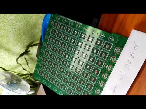
Carbon ink PCB (printed circuit board) is coated on the PCB substrate with carbon-based conductive ink (referred to as carbon ink), cured to form a PCB with a carbon film conductive pattern. Now the market’s requirements for PCB board production costs have dropped repeatedly, and it is a general trend to use carbon oil keys to replace the current expensive gold keys. Carbon oil board is a relatively common surface treatment method for single and double PCBs. Through a series of inspections, tests and aging tests, and other technical processes, the PCB can work reliably for a long time.
1.The composition of carbon oil
Carbon oil is mainly composed of synthetic resin, hardener, and carbon powder.
The synthetic resin plays a role in adhesion (equivalent to a carrier).
The hardener plays the role of curing.
Carbon powder plays a conductive role (graphite powder can be added, but with high cost).
Some suppliers add a little silver oil into the carbon oil to obtain lower resistance and higher conductivity.
2.The resistance of carbon ink
The resistance of carbon oil is generally expressed by square resistance. Some use ohms per square centimeter (Ω/cm²), and some use ohms per square centimeter (Ω/□). Most suppliers now agree to use Ω/□.
Square resistance refers to the resistance value of any square carbon film on the opposite side, which is related to the thickness and composition of the carbon oil. (It can be analyzed from the figure below).
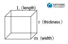
According to Ohm’s law:
R=ρ*L/S (R=square resistance, ρ=resistivity, L=carbon oil length, S=side area=thickness*width=r*m)So R=ρ*L/r*m(if L=m)So R=ρ*r
It can be seen from the above formula that when the surface impedance is L=W (when the length and width are equal, any square “□”), it can be expressed by “Ω/□”. But it must be stated at what thickness is the “Ω/□” value. Generally, the supplier will indicate ≤ 30Ω/□ at 15um or 25um.
3. The resistance control of carbon oil
The resistance of carbon oil is only related to its composition and thickness. Therefore, to obtain a satisfactory resistance requirement, we must follow three aspects.
1) A reasonable square resistance carbon oil that meets the process requirements.
2) A reasonable thickness (0.01-0.025mm) should be achieved after printing.
3) Baked fully (oven: 150℃ to 170℃, for 30-60 minutes; infrared oven: 150℃, for 15 minutes).
In the actual operation process, the temperature is high, the time is long, and the square resistance is low. It is important to choose a reasonable temperature and time without affecting the substrate.
More Reading Guides
The characteristics and uses of carbon ink PCB
The carbon ink has strong adhesion, peeling resistance, and strong abrasion resistance, which can reach ≥ 1 million times, and the resistance change rate is ≤ 10%. The square resistance of conductive paste is relatively large compared to other metals. The square resistance of the current carbon oil board can generally be controlled at ≤ 20 ohms, but the cost is low with a high-performance cost ratio. The conductive paste is a crucial material for electronic component packaging, electrodes, and interconnection of electronic components. It mainly includes two types: burn-in conductive paste and curing conductive adhesive (conductive ink).
Carbon ink board use:
Carbon oil board is mainly used in film circuits, mobile phone soft circuits, medical devices, communication equipment, automotive electronics, smart label RFID, and many other industries. In the circuit board industry, it is mainly used for calculators and remote controls. It can replace copper-plated holes, silver slurry hole fillings, and the copper slurry hole filling process. Environmental protection and the low cost of carbon slurry hole filling is the mainstream trend of the development of circuit boards. Currently, Microsoft uses carbon oil filling holes on the power supply board, which can completely replace the double-layer board with copper-plated holes.
Printing carbon oil production capacity
1. Carbon ink gap:
Since carbon oil has good electrical conductivity, the carbon oil on the finished board needs a gap to ensure that there is no short circuit. Usually, the minimum gap should be 8mil (HOZ bottom copper) and 12mil (1-3oz bottom copper) for the finished product. If opening a film, then the gap should increase.
2. Carbon oil minimum alignment tolerance: +/-6mil
3. The size of the carbon oil window and the gap between the copper pattern: Due to the alignment tolerance and oil leakage and to ensure copper is not exposed, the carbon oil must be 6mil (HOZ bottom copper) or 8mil (1-3OZ bottom copper) larger than the copper pad on one side. Correspondingly, a gap of 6 mil (HOZ bottom copper) and 8 mil (1-3OZ bottom copper) between the carbon oil window and the surrounding copper pattern is required. This is to prevent carbon oil from covering the surrounding copper pattern, to avoid short circuits.
4. Carbon oil thickness
The first screen printing carbon oil thickness: 0.3-1.0mil, tolerance: +/-0.3mil. If the thickness of the carbon oil is required to be 1.0mil or more, the carbon oil needs to be reprinted twice. The second reprinted carbon oil thickness: 1.0-2.0mil, tolerance: +/-0.4mil. The second reprint carbon oil film is 3mil smaller than the first, so two sets of tools need to be written on MI.
The process parameter description of carbon oil PCB
| Requirements specification | Marginal data |
| Minimum line spacing: 0.25mm | |
| Minimum line width : 0.25mm | |
| Distance between the copper wire and board edge: 0.5mm | |
| The pad of through-hole: Carbon flybridge 1.0mm, carbon through-hole 1.6mm | |
| Plug-in pad: More than 0.8mm larger than the overall aperture | |
| The gap between pad to copper wire:0.5mm | |
| The gap between pad to pad: 0.5mm | |
| The min Plug-in hole: 0.7mm | |
| The min SMD pad:1.0mm | |
| Minimum line width of carbon film button: 0.5mm, Min line gap: 0.5mmMinimum line width of carbon film jumper: 1.0mm, Min line gap: 0.6mm | |
| The gap between all holes and board edge: more than 1.5mm |
In addition:
- The finger distance of the carbon bond can be adjusted appropriately to ensure the same distance.
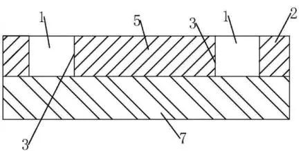
- Do not increase the carbon key size and the fingers’ width. The length of the fingers can be appropriately shortened to ensure sufficient spacing (figure 1: 0.40mm or more). The fingers’ width can also be slightly reduced (try to keep it within 10%).
3. A: If copper fingers are under the carbon keys, the copper fingers can be reduced appropriately to ensure no copper is exposed. The minimum width of the copper fingers (a) is 0.12mm, and the connection function (b) must be 0.25mm. (See Figure 1)
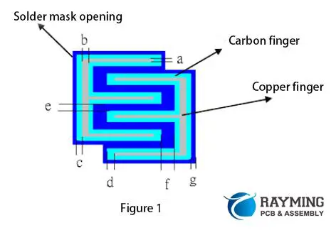
carbon fiber pcb
Copper finger line width a=0.12MM
Copper finger line width b=0.25MM
Carbon oil cover copper c=0.20MM (min 0.15MM)
Carbon oil cover copper d=0.25MM (min 0.20MM)
Carbon oil spacing e=0.40MM (min 0.30MM)
Carbon oil spacing f=0.60MM (min 0.40MM)
The solder mask opening of the carbon oil button g=0.15MM
B: There is no copper finger under the carbon bond, only the contact point. If the carbon contact point is less than 1.10MM, you can increase slightly; try not to exceed 0.10MM on one side. Changing the line is unnecessary, only reducing the green solder mask opening but ensuring that copper is not exposed. The minimum width of the contact point solder mask opening is 0.60MM (usually 0.80MM or more), but it should be as large as possible. (Same as carbon bridge). Please refer to Figure 2:
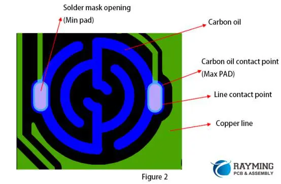
The carbon oil contact pad is larger than the solder mask opening by 0.20mm on one side (min 0.15mm).
Insulating oil and protective oil
- The insulating oil process takes place before the carbon oil, and the protective oil process is after the carbon oil.
- When making insulating oil and protective oil, it should be more than 0.50MM larger than carbon oil on one side.
- The minimum distance between the insulating and protective oil and the solder mask opening pad is 0.25mm (generally 0.30mm).
- Insulating oil: The carbon contact should be shaved at least 0.10mm from one side of the line pad. Same as all the solder mask opening. Protective oil: It is not necessary to shave solder mask opening on the carbon contact; cover the carbon bridge, and shave others. The buttons area must also be shaved, and the distance from the buttons is more than 0.30mm.
- When there is text on the carbon oil surface, and the protective oil is white. The text cannot overlap with the protective oil, and we should remove the text or shave the protective oil according to the specific situation. However, we need to ensure the protective oil can cap carbon oil more than 0.30MM.
Carbon/silver ink through-hole film
- 1. The method of carbon/silver ink through-hole film is similar to that of carbon bridge. For specific data, please refer to Figure 3:

From the edge of the hole to the solder mask opening a=0.25MM (min0.20MM) (Contact size of carbon oil and copper)
Carbon oil cover green oil b=0.10MM (The minimum is as large as green oil)
From the edge of the solder mask opening to line pad C>0.00MM (more than 0.10mm)
- Carbon/silver oil-filled orifice plates should make protective oil, which is required to be larger than the carbon/silver oil pad by 0.50mm on one side and 0.30mm away from other solder mask opening pads.
Process control of carbon ink board
The process control of the carbon oil board in the silkscreen room is straightforward. Let’s take a look at the following aspects together:
1. Operators must wear gloves to work.
2. During the production operation, the process parameters of each machine and equipment must be carried out according to the relevant operating instructions and shall not be changed.
3. All machines and equipment must be clean. There must be no dust, garbage, oil, and other debris on the surface.
4. The speed of screen printing and the suction pressure of ink return should be controlled according to operation procedures (Based on the printing effect).
5. The screen mesh, scraper, and carbon oil should be selected per the requirements of the engineering MI.
6. The carbon oil must be stirred evenly before use. Use a viscometer to detect that the viscosity is within the required range, and seal the cover immediately after the ink is used.
7. The oil, oxides, and other pollutants on the board must be cleaned before printing. All carbon oil boards must be confirmed by QA before moving to the production line.
8. In the process of screen printing, the operator must self-check at least 2PNL for each printed board. In special cases, the operator might need to increase the number of self-check.
9. For carbon oil resistance measurement, the resistance value of the carbon oil through-hole should be less than 100 ohms, the square resistance of the carbon wire should be less than 25 Ω/口 (carbon wire length ÷ carbon wire width × 25 Ω), and the oil passing through the carbon oil hole should be more than 2/3. The resistance can be tested according to the drawings of the engineering department and the MI requirements.
10. The operator should record the time and temperature of each baking board. The operator should also inform QA to do spot checks of carbon resistance value and adhesion test after cooling.
- 11. Each carbon-oil screen plate must be returned to the screen room for re-printing after 2500 uses.
There are many safety precautions for the carbon oil board in the silkscreen room. Let’s talk about two of them.
1. Do not put your hand or body into the screen when opening the machine.
2. Baking board operators should wear thick-line gloves to prevent skin scalding.
The problems and solutions in the carbon ink production process:
- Exposed copper
There are carbon bridges and carbon oil buttons on common single-layer PCB carbon oil printing. Some customers have designed copper circuits under the carbon oil buttons. If there is copper under the carbon oil keys, it is easy to expose copper during production. In order to avoid copper exposure, it is necessary to pay attention to the following four factors.
- Design factor: Mentioned above.
- Substrate sheet factor: After cutting lamination, If there is a carbon key board, it must be shrunk before printing. Generally, the thickness of the 1.2mm board is baked at 120℃ for 80 minutes, and the 1.6mm board is baked at 120℃ for 90 minutes. If shrinkage treatment is not conducted before printing, the board will shrink after etching, grinding, green solder mask, and carbon oil bridge process. If pre-shrinkage treatment is done in advance, the shrinkage will be minimal in production.
Therefore, the circuit fingers will change irregularly and move positions without shrinking treatment, and the carbon oil film is fixed; finally, the copper was exposed. After the previous procedures are all completed, the carbon oil film should be put together according to this sheet and not the line film.
- Printing method:
①When printing carbon oil, it is necessary to follow the line direction.
②The printing area should not be too large.
- Leakage Current (poor insulation, micro short circuit)
- The copper powder between the lines causes leakage. Since the grinding pressure is too big or the direction is not correct, the copper powder remains between the lines. In a dry environment, these copper powders will not produce undesirable phenomena, but there will be micro-short circuits during electroplating in a humid environment. Therefore, it is necessary to control the grinding pressure and direction.
- Due to the close distance between the button bits, the oil leaks during printing which causes electric leakage. Also, please pay attention to the direction when printing.
- The green oil solder mask factors:
There is too much garbage in green oil or bridge oil, and some of the garbage may produce conductivity. Therefore, the screen mesh of bridge oil should not be too small (generally 90-120T), and the environment should be kept clean.
- Technical treatment of the line direction under the carbon oil bridge:
Due to the scraper printing machine’s limitation, the line under the carbon oil bridge must be kept straight and not curved, so there will be no oil at the curve of the green oil and bridge oil solder mask. If this phenomenon occurs, it must be corrected to reduce the hidden danger of copper exposure during printing.
- Printing direction of bridge oil
If there is a carbon bridge, you must add bridge oil. If you only print the green oil once, there will be some small pinholes so that the carbon oil will cause a short circuit with the wiring below. The bridge oil generally needs to be printed twice. The second time, it needs to be printed in the opposite direction (90° or 180°) to reduce copper exposure and be insulated entirely.
- There are mainly the following reasons why bridge oil cracks lead to leakage:
- The peel force strength of green oil.
- A vacancy is formed at the edge of the electroplated plate line due to side etching.
- The board is bent.
- Leakage not caused by carbon oil
Some boards have high water absorption, which may be acceptable in a dry environment. However, they will cause a short circuit between the lines due to water absorption when they are damp.
- Analysis of the reason for carbon ink fracture
- Over-addition of diluent leads to crack of carbon oil bridge
Under normal circumstances, carbon oil can be used directly without adding a diluent. To diluent the carbon oil, you must add the special diluent in the correct proportion. If you add too much at will, the viscosity of the carbon oil will be significantly reduced. As a result, the board will crack and result in a high resistance or even a completely open circuit. The correct way is to add diluent as required by the supplier.
- The baking temperature is not set properly
If the carbon oil is rapidly baked at a high temperature after silkscreen, there will be a difference in heating between the carbon oil on the line and other places. As a result, cracks will occur during curing. In order to avoid this situation as much as possible, the carbon oil can be properly extended for parking time after the silkscreen, and the temperature should be slowly raised in the oven.
Therefore, in the actual production process, the following points must be achieved:
- The key bit board must be shrunk.
- The film with buttons on the line must be modified (the width of the copper wire should be smaller than the width of the carbon wire).
- The baking temperature should be from low to high.
- The dilution of the ink must be operated in accordance with the instructions.
- The printing direction of the bridge oil should be opposite and use the same type of ink.
- In order to avoid breaking the bridge oil, the printing does not need to bend the board.
- The mold should be hollowed out to avoid crushing the bridge oil.
The carbon oil PCB manufacturer printing is an environmentally friendly process that will not pollute the air, water, soil, etc. We believe more engineers will choose the carbon oil grouting-hole process to replace the copper-plated hole process when designing in the future. Everyone in our global village loves our planet, and everyone is responsible for protecting it. What we can do now is to protect our planet with environmental-friendly PCB designs. We believe that carbon oil grouting is an industry trend.
Come on, protecting the earth starts with the carbonized design!