Altium Designer is one of the most widely used printed circuit board (PCB) design software packages worldwide. This comprehensive article covers Altium Designer pricing and licensing options, free trial and full downloads, and a beginner tutorial on installing and using Altium Designer for the first time.
Introduction to Altium Designer
Altium Designer is a premium, professional-grade PCB and electronic product design software platform created by Altium LLC. Some key features include:
- PCB design and layout with intelligent autorouting
- Integrated 3D modeling for mechanical CAD collaboration
- Circuit simulation and signal integrity analysis
- Version control, supply chain and product lifecycle management
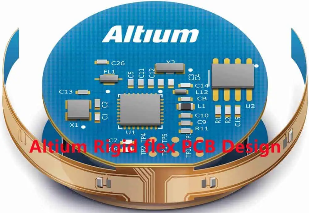
- Support for high-speed design, flex/rigid flex boards
- Native support for MCAD file formats like STEP and IGES
- Built-in library management and component database
Altium Designer aims to provide an end-to-end electronics design workflow in a unified environment. It competes with other premium PCB design software like Cadence Allegro and Mentor Graphics Xpedition.
Now let’s explore Altium Designer pricing options, free trials, full downloads and beginner tutorials.
Altium Designer Pricing and Licensing

Altium offers various pricing tiers and licensing options for Altium Designer to suit different customer needs:
Subscription License
A subscription license provides temporary access to Altium Designer for a recurring fee billed monthly or annually. It allows flexible scaling of seats as needs change.
Pricing:
- 1 month: $245/month
- 12 months: $180/month when billed annually
- Volume discounts available for multiple seats
Perpetual License
A perpetual license provides permanent access to the version purchased. A maintenance plan is required to receive updates and support.
Pricing:
- Base license: $10,000
- Additional seats discounted ($7000 each)
- Annual maintenance plan: roughly 20% of license cost
Free Trial License
A fully functional, time-limited free trial allows evaluating Altium Designer’s capabilities firsthand.
- 15 day free trial available
- No payment information required
Academic pricing is also available for students and educational institutions. Consult Altium sales for current rates, discounts and collaborative licensing options.
Now let’s look at how to download, install and begin using Altium Designer.
Downloading and Installing Altium Designer
Several options exist for downloading Altium Designer:
Free Trial Download
A 15 day free trial of the latest Altium Designer version can be downloaded from:
https://www.altium.com/free-trial
The large download is around 5GB. An internet connection is required to validate the free trial license upon first use.
Subscription Installer
For the subscription version, Altium provides an installer download that streams the needed components as you use them. This allows a lighter initial install and more flexibility:
https://www.altium.com/solutions/electronic-design-software/altium-designer
Offline Installer
For situations with slow or no internet access, a full offline installer can be downloaded as well after signing in with an active subscription or permanent license.
The offline download is around 12GB in size. An internet connection is still periodically needed to validate the license.
Once Altium Designer is downloaded, run the installer (.exe file) and follow the step-by-step prompts to complete the installation process on your Windows PC.
Exploring Altium Designer for the First Time
The first time Altium Designer is launched, a modal dialog appears for activating a license. Sign in with your Altium account credentials or activate a free trial license.
Next, select a template. The “PCB Project” template is a good starting point as it includes both a PCB layout and corresponding schematic document.
Finally, a “Learn & Discover” introductory tour pops up. Take a few minutes to browse this interactive tutorial explaining Altium Designer’s interface and key capabilities.
When ready to dive in, the PCB editor will open by default to a simple sample layout. The dark interface theme and green accents match Altium’s branding.
Now let’s take a closer look at Altium Designer’s key parts and initial settings.
Altium Designer Interface Tour
Altium Designer’s main interface includes several key elements:
- Menu Bar – Access to all features and commands. Recently used are pinned on right.
- Toolbars – Frequently used actions like layout commands.
- PCB Editor – Main design canvas for 2D/3D PCB layout.
- Inspector Panels – Settings and properties for items selected in the editor.
- Panels – Tabs like Projects or Libraries to browse project documents and design elements.
- Notifications – Messages like errors and warnings appear subtly on lower right.
- Status Bar – Information like cursor coordinates and design rule checks.
The interface adopts a dark color theme with green highlights by default. This can be changed in Preferences based on personal taste.
Next let’s adjust some preferences in Altium Designer.
Configuring Preferences in Altium
Many design settings and options can be configured in Altium Designer’s Preferences dialog. Go to Design > Preferences or press Ctrl+G to access them.
Key settings groups to check include:
- System – General options like language and auto save.
- Schematic – Options for schematic sheets, wires and other objects.
- PCB Editor – Defaults for PCB layout, routing and display.
- Data Management – Setup for connecting to version control or PLM systems.
For example, under System Preferences > User Interface, the overall theme and color scheme can be adjusted to your liking.
Poke around the different sections to get a feel for what settings are available in Preferences as you start to use Altium. Options can always be changed later as you gain experience.
Now let’s create a new schematic and PCB layout document.
Creating a New Schematic and PCB

To create a new blank schematic and PCB layout document in Altium Designer:
- Click File > New > Project > PCB Project
- Enter a project name like “MyFirstProject”
- Click the Target Project Location drop down and browse to where the project files should be stored.
- Ensure the “Add Schematic and PCB Files” box is checked.
- Click Create Project
This will generate a new project with empty SCHDOC and PCBDOC documents ready for designing a basic two-layer circuit board.
Now we’re ready to start adding components and wiring up a schematic!
Placing Components in the Schematic
To begin putting together a circuit schematic in Altium:
- Select the Schematic Library panel tab, expand the integrated library, and locate components to add.
- Select a part like the common LM358 op amp.
- Click to place it on the schematic sheet (it may auto-rotate).
- Repeat to place additional parts like resistors, caps, wires and pins.
- Use the Wiring Tool to connect component pins with wires.
- Double click a part to edit its properties and parameter values.
Use the browser-like Schematic Libraries panel to place components, then wire them up!
Altium includes a large set of prebuilt schematic symbols and PCB footprints in its integrated libraries. Now let’s build a simple circuit.
Schematic Capture Example
Let’s create a basic schematic for a voltage divider circuit to see core symbol placement and wiring in action.
- Place two resistors R1 and R2.
- Place Ground and Voltage Source schematic symbols.
- Use the Wiring tool to connect the components as shown:
- Double click R1 and R2 to change resistance values, say to 10K and 1K.
- Add net/wire labels like “Vout”.
With just a few clicks, a functional schematic comes together! Now we can transfer this to a PCB layout.
Generating a PCB from the Schematic
Once a schematic is completed in Altium Designer, generating the initial board outline and component placement on the PCB layout is straightforward:
- Switch from the schematic editor to the PCB editor.
- With the PCB document open, choose Design > Update PCB.
- In the dialog, select the source schematic sheet and click OK.
- The PCB will auto-populate with components from the schematic.
The synchronization goes both ways – from schematic to PCB, and from PCB changes back to the schematic. This bi-directional updating is a key benefit of Altium Designer.
Now let’s explore PCB layout editing and routing.
PCB Layout Editing in Altium
With the board outline and components imported, we can begin arranging parts and routing connections on the PCB.
On the PCB editor, parts can be moved either interactively or by changing X/Y coordinates in the Inspector panel.
To route connections between component pads:
- Select Place > Route from the menu.
- Set the desired trace width and routing layers (Top, Bottom, etc).
- Click on pads to insert linear trace segments. Right-angle corners are inserted automatically.
- Complete tracing a connection by clicking the final pad.
- Press Esc or click the Route button again when routing is complete.
Let’s route out the simple voltage divider circuit from the earlier schematic.
PCB Layout and Routing
Here is how the PCB editor looks after arranging parts and manually routing traces for the basic voltage divider:
With copper traces wired up, the electrical connections are complete. The PCB could be sent for fabrication at this point if desired!
Next we’ll use Altium’s auto router to more efficiently complete connections.
Auto Routing in Altium
Manually routing an intricate PCB layout can be extremely tedious. Altium Designer has an intelligent auto router to route connections rapidly:
- Ensure all desired nets are named to guide the auto router.
- Set routing layers allowed (Top, Bottom, etc).
- Choose auto routing options like follow manual traces.
- Run the auto router (Route > Interactive Routing > Auto Route).
- The auto router will intelligently work to route remaining traces.
- Tidy up traces or manually finish any incomplete connections.
With a mix of manual and auto routing, even large complex PCBs can be wired up very efficiently. The auto router helps finish the tedious parts.
For more advanced functionality like design rule checking, 3D modeling and manufacturing outputs, explore the many in-depth tutorials on Altium’s website and YouTube channel. The built-in help documentation also provides excellent feature explanations and examples.
Summary of Key Features
To recap, core Altium Designer capabilities as explored in this introductory tutorial include:
- Unified, highly integrated schematic and PCB design environment.
- Placement of components from schematic libraries.
- Wiring up circuits and networks.
- Synchronization between schematic and PCB.
- Manual and intelligent auto routing of board traces.
- Extensive component libraries and design reference materials.
There is much more to learn. But this basic tutorial illustrates how even a beginner can start creating schematics and circuit boards in Altium Designer quickly.
Altium Designer Guide and Resources
To leverage Altium Designer’s advanced features and streamlined workflows for electronics product development, consult the following resources:
Learning Guides – Altium offers free Designer Courses introducing key features and workflows:
https://www.altium.com/free-designer-courses
Documentation – Search the extensive documentation for detailed explanations of every Altium Designer capability:
https://docs.altium.com/display/ADRR/
https://www.altium.com/blog/tag/resources
YouTube Channel – Altium’s channel features tutorials on advanced workflows and methodologies:
https://www.youtube.com/user/AltiumLive/videos
With its comprehensive features, high integration and smart automation, Altium Designer helps streamline and accelerate the PCB design process. For engineers looking to master professional-grade electronics product development workflows, Altium Designer is a very worthwhile investment.
Frequently Asked Questions
What are the main advantages of Altium Designer compared to low cost PCB design software?
Key advantages of Altium Designer versus entry-level tools like Eagle, KiCad or EasyEDA include:
- Unified environment for schematic capture and PCB layout
- Automated ECO changes synchronize schematics and boards
- Advanced auto-routing for highly efficient trace wiring
- Built-in 3D modeling and MCAD collaboration
- Scripting and customization capabilities
- Seamless version control and supply chain integrations
- Access to component libraries and virtual components
The advanced capabilities justify the higher cost for professional users.
What skills are required to start using Altium Designer as a beginner?
To get started with Altium Designer as a new user, having general experience with:
- Electrical engineering and schematic diagrams
- Electronic components and PCB basics
- Drafting and drawing board layouts
- Using windows-based CAD software
will help tremendously. No prior experience with Altium or PCB design software is required. Altium provides documentation and videos tailored for first-time users of the platform.
What resources are available for learning more about Altium Designer?
The key resources available for learning Altium Designer in depth include:
- Free training courses on Altium’s website
- Documentation searchable by capabilities and features
- Blogs and forum discussions
- Official YouTube channel with tutorials
- Altium’s monthly newsletter and design content
- Live seminars and conference events
Between the software itself, built-in help, and wealth of training materials, there are excellent resources to master Altium Designer.