Find a High Volume PCB Manufacturer and Supplier. Choose Quality High Volume PCB Manufacturers, Suppliers, Exporters at RayPCB.com.Welcome to send your design to Sales@raypcb.com
High Volume PCB Production Manufacturing
1. The RayMing Guarantee
Thinking of PCB Manufacturing with your PCB purchasing? Use RayMing as your go to partner. If there is ever a disruption in your supply chain we have you covered with our manufacturing facility as a backup with competitive prices. So you never have to worry again. Secure your supply chain with RayMing.
RayMing capabilities provide:
Quicker Delivery
Higher Quality
Cost Reduction
Increased flexibility
Seamless facilitation
Supply chain security
Engineering and Technical support
Excellent Customer Service
Account Representation
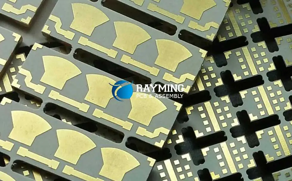
2. High Lever PCB Equipments to secure your high volume PCB orders
3.Very Strict Quality Control to ensure steady quality PCB delivery
4. 7 x 24 Hours , Customer Services Stand-By
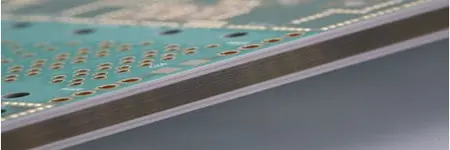
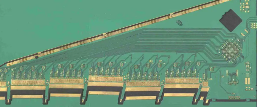
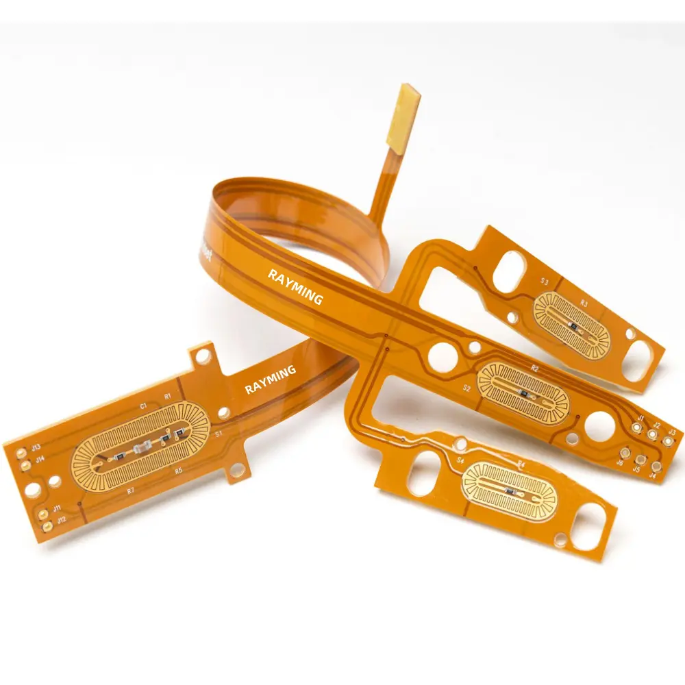
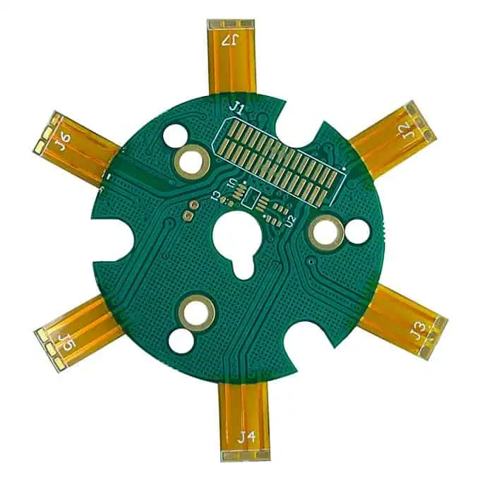
Our high volume PCB manufacturing including Flexible PCB,Led PCB , Rigid-Flex PCB,Rogers PCB and so on, If you have such high volume PCB order, Pls send to quote .
All You Need to Know about High Volume PCB
Circuit boards have become a key cog of every electronic equipment and device in the present-day world. Considering our ever-increasing reliance on electronics for diverse purposes starting from our homes to our workplaces, then the importance of circuit boards will only but increase with time. It is something that I find fascinating considering the evolution of circuit boards from the breadboard days to the new complex, miniaturized printed circuit boards.
Our overreliance on printed circuit boards for our electronic needs calls for a high volume PCB assembly and PCB mass production. Because of this, it not only becomes crucial to undertake high volume PCB production and get an ideal high volume PCB manufacturer to cater to these needs. This article canvasses all the key aspects you need to know about high-volume printed circuit boards. So let us dig in, shall we?
High Volume PCB Production and Assembly
The subject of high volume PCB production and assembly can often prove confusing for both experienced and fresh faces in the circuit board industry. For starters, therefore, it becomes essential to detail what high volume PCB production and assembly refers to and get it out of the way. So what is it all about?
- High Volume PCB Production
High volume PCB production refers to the last step of the circuit board production process before delivery to customers or clients. It always features no design changes with a linear process that results in large volumes of printed circuit boards. The aim of this process entails producing high volumes of PCBs as required by the client at the least costs, albeit with a high yield rate.
- High Volume PCB Assembly
High volume PCB assembly implies the assembly of printed circuit boards of ten thousand plus pieces with DFT and DFM. Such a high number requires you to understand what type of PCB you want before engaging a PCB company for your mass PCB needs. Otherwise, you can end up with large PCB of excellent quality that cannot help your electronic needs. Therefore, the significance of picking the right printed circuit board cannot get understated, especially when it comes to influencing the performance of your electronic product.
What better-printed circuit board manufacturing company to engage for your high volume PCB production and assembly needs than the RayMing PCB and Assembly Company? The company will not only guarantee your mass PCB supply needs through its manufacturing facility but wow you with its printed circuit board capacity in aspects like quick delivery, cost reduction, etc. Additionally, the company possesses high lever printed circuit board equipment to secure your orders, adhere to stringent quality control measures in delivering high-quality printed circuit boards. What’s more, the company has a round-the-clock customer support service to ensure a seamless experience during the high volume PCB production and assembly process.
Maximizing the PCB Production and Assembly Process
In most instances, if not all, maximizing the high volume PCB production and assembly process efficiency often hinges on optimizing the low volume production process. So to maximize the high volume production and assembly process, it becomes imperative to maximize the printed circuit board prototyping phase. So how can you ensure this?
- Pick a qualified contract manufacturer for your printed circuit board design. The quality of low volume PCB production often hinges on the contract manufacturer’s expertise and equipment in meeting your design needs.
- Tailor your PCB design to your contract manufacturer’s capabilities. It becomes essential to use specifications that align with the contract manufacturer’s equipment capabilities to ensure timely deliveries, prevent the need for redesigning, and avoid extra development costs.
- Optimize the selection of your components. A shortage of components often proves a common reason for stalled or disrupted production. It, therefore, becomes pivotal to ensure that all crucial components (of acceptable quality) are available for your anticipated production levels.
- Apply decent DFM (design for manufacturing) guidelines. It becomes crucial to assist the low-level production of your printed circuit boards by following design for manufacturing guidelines and rules specific to your contract manufacturer. It will, in turn, help with your high-volume PCB production and assembly process.
- Perform the required testing of the printed circuit boards. It becomes vital to ensure that every regulatory testing gets conducted on your printed circuit boards post the prototyping stage. However, you should always try and go beyond by performing extra tests to ensure aspects like structural integrity prove sound.
If you optimize the low volume production phase by sticking to the detailed aspects, you will optimize your printed circuit boards’ high volume production and assembly process. Here, it becomes essential to remember that the initial stages of the production process prove essential as it acts as the basis for the high volume PCB production and assembly.
Easing the Transition from Low Volume/Prototyping to High Volume Printed Circuit Board Production

You sure understand the importance of PCBs and how the prototyping stage and its optimization impact high volume PCB production. So what happens during the transition process, and how can you seamlessly transition from prototyping to high volume mass production.
Like in most other real-life situations, the transition from low volume to mass production can prove difficult, though it always comes with incredible gain. In electronics, this prototype-to-mass production transition often proves a significant one. While the base unit remains constant from the prototype level to the high volume production of printed circuit boards, the specific processes often prove unique with particular objectives.
Becoming aware of the differences between the objectives becomes pivotal for engineers and designers of PCBs when picking the ideal contract manufacturer for the two product development phases. Additionally, such knowledge also becomes invaluable in easing the transition from the low volume/prototype phase into the mass or high volume production phase.
Before we delve into the transition process, it becomes necessary to understand what PCB prototyping and high volume production imply. Firstly, the prototyping of PCBs infers the development of small quantities of printed circuit boards that can get deployed for design validation processes by testing the system’s performance and operation. Therefore, the process must feature aspects such as flexibility, prove sufficiently fast, and get carried out by quality contract manufacturers besides consistent testing. At this stage, any design issues get corrected to avoid any issues on the development of the printed circuit board or post-production in its lifecycle when deployed.
Conversely, high volume PCB production aims at reliably and efficiently producing high-quality printed circuit boards. The assumption at this stage always encompasses aspects such as the components, design, operation, and functionality having gotten sorted out in the prototyping phase. Because of this, the focus during high volume PCB production revolves around attributes such as reliability, testing, and cost-effectiveness.
Reliability becomes key because of the large number of printed circuit boards involved that must prove similar in design and quality and at a high yield rate. On the other hand, testing becomes crucial because of ensuring high-quality standards of the PCBs post-production. Finally, the cost aspect becomes crucial because of the large quantity of printed circuit board units. The large number ensures lower costs of production utilizing the principle of economies of scale.
It, therefore, becomes apparent that the objectives between prototyping of PCBs and mass production/high volume production are different. Consequently, transitioning from one phase to the other will require numerous changes, which include contract manufacturers (when the CM specializes in either of the two). However, it is important to state that if you contact us at RayMing PCB and Assembly, you will not need to change and contract another firm as we cover both aspects.
The Transition from Prototyping to High Volume Production of Printed Circuit Boards
The transition from the PCB prototyping phase into mass/high volume production must prove seamless and direct in ideal circumstances. However, the transition is never as seamless as everyone would want. Here, you can face countless challenges, such as the need for readjustment of the design files to facilitate quality printed circuit boards. However, the absence of such files can become costly as you will spend more time and money to rectify and produce quality PCBs by having to make engineering design changes.
Other crucial issues that may arise in the absence of design files include the need to obtain and submit extra design files from your prototype manufacturer to the contract manufacturer. Additionally, your contract manufacturer may lack the capacity to develop your circuit boards in line with similar specifications detailed by your prototype contract manufacturer. It also becomes typical to find components missing even during the PCB production phase. Finally, design changes may become necessary, especially when under performance and operational inadequacies need re-prototyping and redesigning.
Such issues, when they crop up, can delay the high volume PCB production process because of the countless redesign needs you will have to do before the mass production. While it may not always seem possible to resolve or avert all the potential issues that might crop up, it becomes possible to ease the transition by adopting some crucial PCB product development process guidelines. So how can you ease the transition process from the prototyping phase into the high volume production process?
The best way of ensuring a smooth transition from prototyping into high volume production of printed circuit boards entail finding and picking a contract manufacturer willing to collaborate in creating an excellent final prototype design besides as-built design files to eradicate the need for engineering change order and therefore speed up the high volume production process.
Benefits of Mass/High Volume PCB Assembly
The benefits that accrue from a high volume printed circuit board are numerous and significant. The benefits include the following.
- High volume printed circuit board assembly encompasses the need for the prototyping and design functions to get carried out in one go, ensuring that the prototype gets meticulously developed and tested to guarantee accurate functioning. Therefore, it becomes simple to get the large production run going.
- The high volume PCB assembly ensures mass production of printed circuit board products, something that becomes incredibly useful in going to market at a mass or large-scale level. It ensures large numbers of quality printed circuit board products and quick turnaround periods. Such a situation proves ideal for getting to the market quickly and ahead of the existing competition.
- Another incredible benefit of high volume printed circuit board production entails the aspect of low production cost. Many cost-related benefits accrue from engaging in a high volume printed circuit board production as high volumes often result in economies of scale. The production cost will impact the pricing of your printed circuit board which enhances your competitive edge in the electronics market. It acts differently from an instance where you produce and assemble small batches, as this always tends to increase the cost.
- High-volume printed circuit board production and assembly also provide a shortened production cycle, all thanks to automation. Therefore, it plays a major role in your production pipeline and the go-to-market strategy, which gets a major boost.
- The mass or high volume production of printed circuit boards also ensures the production consistency and uniformity in features. It results from a scenario that the assembly of each printed circuit board gets a similar assembly and testing regime, which in turn guarantees the quality.
Application Areas of High Volume Printed Circuit Board Assembly Services
- High-volume printed circuit board assembly services apply in the mass production of electronic appliances.
- Under typical circumstances, the entry process into new or existing markets in diverse geographical areas requires large-scale printed circuit boards. Because of this, high volume PCB assembly services apply significantly.
- Mass volumes of PCBs also find application immediately printed circuit boards go beyond the prototype phase of the development, and once every error, if any, gets corrected. It especially becomes essential before the PCBs get to the market. Because of this, it features prominently in the electronic manufacturing sphere, especially for companies where consistency and uniformity prove key.
Final Thoughts
Printed circuit boards come as an incredibly significant part of electronics, with their manufacturing and assembly become pivotal for every circuit board enthusiast. Because of this, high volume printed circuit board production and assembly become necessary for every person or company interested in designing, engineering, or enthusiast of electronics and circuit boards. So do you want high-volume PCB production or assembly services? Pick RayMing PCB and Assembly today, and you will enjoy it.