Finger Print Lock Appliactions,Design and Manufacturing

Introduction

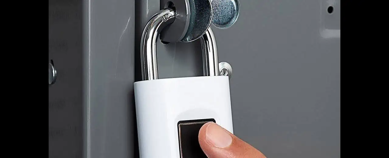
Fingerprint locks, also known as biometric fingerprint locks, are access control devices that use fingerprint recognition technology for locking and unlocking doors, drawers, lockers and more. They offer a convenient and secure unlocking solution compared to keys or combination locks.

In this comprehensive guide, we’ll cover:

  • Applications of fingerprint locks
  • How fingerprint lock technology works
  • Design considerations for fingerprint locks
    • Sensor types
    • Processing
    • Matching algorithms
    • Power options
    • Enclosure design
  • Manufacturing and assembly of components
  • Testing and calibration best practices
  • Advancements in fingerprint locks
  • FAQs

By the end, you’ll understand the full process of engineering fingerprint locks from initial applications, through design, manufacturing, and testing to bring reliable biometric products to market. Let’s get started!

Applications of Fingerprint Locks

Fingerprint locks are used in a diverse range of applications including:

  • Homes and apartments
  • Offices and workspaces
  • Schools and universities
  • Hotels and hospitality
  • Residential care facilities
  • Gyms and sporting venues
  • Laboratories
  • Hospitals and healthcare
  • Law enforcement facilities
  • Financial institutions
  • Sensitive industrial sites

They provide convenient access control in virtually any environment where managing keys or remembering codes poses challenges. Users simply enroll their fingerprint once then unlock reliably and instantly.

Next, we’ll take a technical look inside fingerprint lock design and operation.

How Fingerprint Lock Technology Works

Fingerprint locks function using the following key stages:
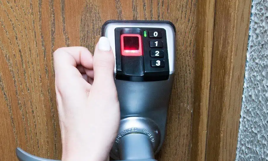
Fingerprint Capture

The user places their finger on the fingerprint sensor. The sensor images the fingertip and captures the fingerprint pattern.

Processing

The processor digitizes the fingerprint image and extracts unique minutiae points as a mathematical representation.

Fingerprint Matching

The extracted fingerprint data gets compared to stored enrollment templates for a match. Advanced matching algorithms are used.

Access Granted

If a match score exceeds the set threshold, the identity is verified and the lock grants access. The door or safe unlocks.

Storage

Users’ enrollment templates get stored in a protected local memory within the lock. Templates should be encrypted.

This provides a high-level overview of key subsystems in a fingerprint lock. Next we’ll look at design considerations and options for each area.

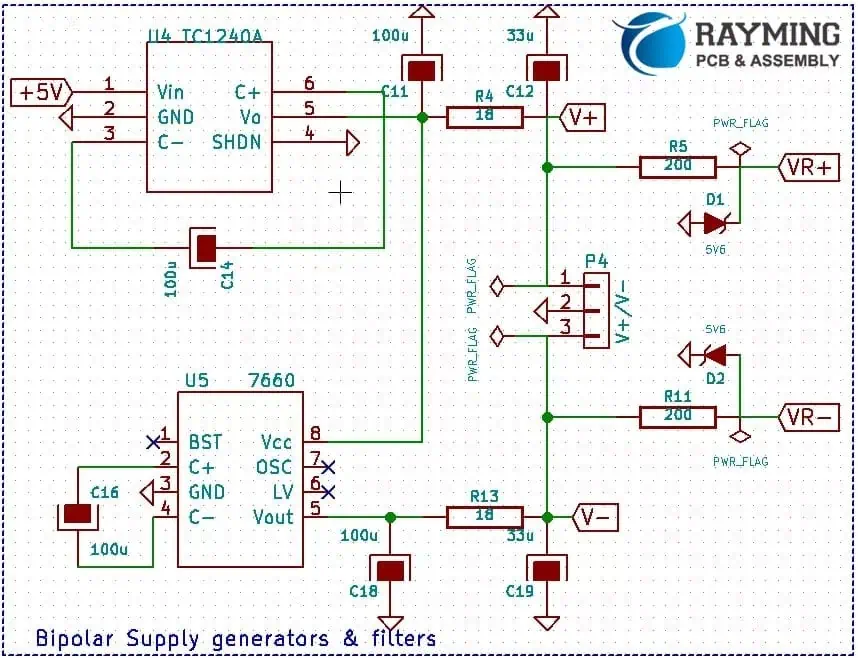
Fingerprint Lock Design Considerations

Designing an effective, reliable fingerprint lock involves careful selection of:

Fingerprint Sensor Type

Two main sensor technologies:

Optical – Uses a camera with illumination to image the fingertip surface. Offers good image quality if sized adequately.

Capacitive – Senses fingerprint ridges using an array tiny capacitors. Compact but more prone to environment impact.

Key tradeoffs: Image quality vs. size. Capacitive suitable for small locks if calibrated well. Optical preferred for highest accuracy in all conditions.
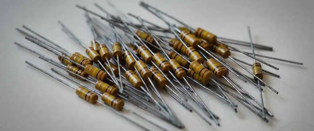
Processing Hardware

A microcontroller or microprocessor is required to process the raw sensor image, extract features, match against templates, control peripherals, etc.

Key factors: Sufficient performance for image processing and matching algorithms, crypto functions for template security, interfaces for peripherals, low power operation. ARM Cortex M4 or faster 32-bit MCUs are commonly used.

Matching Algorithms

The algorithm used to compare the live fingerprint against enrolled templates is crucial for reliable recognition.

Common matching approaches: Minutiae based, ridge feature based, image correlation, machine learning based. A hybrid approach combining minutiae with other advanced techniques often performs best.

Power Supply

A stable, reliable power source is required. Can use:

  • Internal batteries
  • External AC adapter
  • USB power

Battery is convenient but may require periodic charging/replacement. AC powered locks avoid battery issues but need outlet access.

Enclosure

The lock housing must:

  • Protect internal electronics
  • Mount sensor ergonomically
  • Provide mechanical locks/latches
  • Allow accessible wiring
  • Withstand use, weather, tampering

Material, seals, construction must balance function, cost and aesthetics.

Careful engineering of all subsystems results in a robust, usable fingerprint lock that provides convenient biometric access control. Next we’ll look at manufacturing critical components.

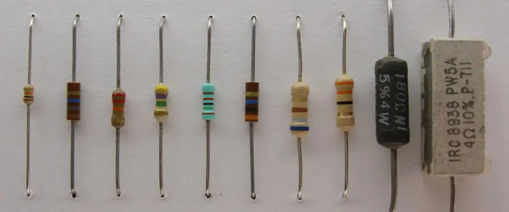
Fingerprint Lock Manufacturing and Assembly

Producing reliable fingerprint locks requires close attention during:

Sensor Manufacturing

The image sensor integrated circuit fabrication process must achieve:

  • High pixel density for detailed imaging
  • Low defect rates to avoid bad pixel clusters
  • ESD protection for fingerprint static discharges

The silicon fabrication facility must maintain extremely clean conditions.

For capacitive sensors, the capacitor array geometry must be uniformly micro-etched with tight alignment.

Processor Sourcing

The processor is typically sourced as a completed IC component. Key aspects:

  • Sourcing from reputable manufacturers like STM, NXP, or ATMEL
  • Order sufficient volume to qualify wafer lot and obtain consistent quality
  • Rigorously validate received units for defects before assembly

Matching Algorithm Optimization

Extensively tuning matching parameters and testing recognition accuracy using datasets of real fingerprints is key.

Lock Assembly

Proper assembly protocols must be followed:

  • ESD control procedures to avoid static discharge damage
  • Component placement following layout design rules
  • Process validations e.g. torque requirements for enclosure screws
  • Periodic quality audits on units from production line

With rigorous manufacturing practices for critical subsystems, reliably functioning fingerprint locks can be produced at scale.

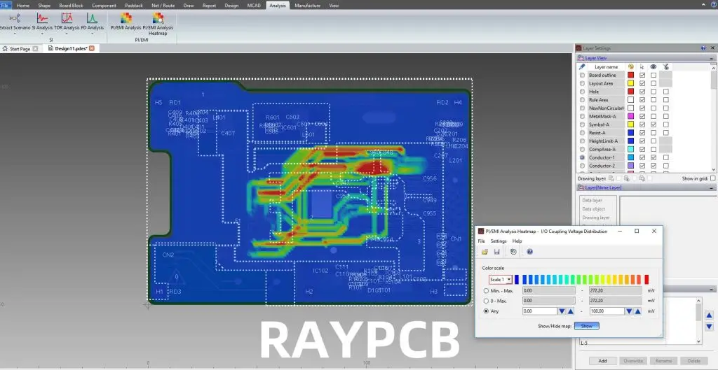
Testing and Calibration Best Practices

To confirm locks operate properly prior to delivery, key testing and calibration steps include:

Unit Testing

  • Verify all electronic components functional
  • Validate processor execution timing
  • Check current draws and power consumption
  • Confirm wired/wireless interfaces working

Sensor Testing

  • Inspect image quality – sharpness, artifacts, distortions
  • Check live finger imaging reliability across conditions
  • Evaluate max image size and resolution

Matching Accuracy Testing

  • Test false reject rate with good fingerprints
  • Validate low false accept rate on invalid fingerprints
  • Tune matching thresholds as needed

Environmental Testing

  • Hot and cold exposure
  • Drop/shock/vibration resilience
  • IP rating validation if relevant

User Testing

  • Sample users enroll and unlock with live fingers
  • Identify any usability pain points

Extensive testing ensures consistent performance and quality for end customers.

Advancements in Fingerprint Lock Technology

Fingerprint lock technology continues advancing:

  • Multimodal – Combining fingerprint sensing with face, iris or other biometrics for multifactor authentication.
  • Anti-Spoofing – Detecting fake fingerprints made from silicon molds etc. Liveness detection can use multispectral imaging and deep learning algorithms.
  • Cryptography – Implementing highly secure methods to store fingerprint data as digital keys unlocks cloud-based access control frameworks.
  • Smart Home Integration – Connecting biometric locks into smart home systems for features like temporary access codes and centralized manageability.
  • Mobile Credentials – Using fingerprints matched on a smartphone in place of direct fingerprint enrollment in each individual lock.

Innovations like these will expand the capabilities and applications for fingerprint lock technology.

Frequently Asked Questions

Here are some common questions about fingerprint locks:

Q: Are fingerprint locks suitable for exterior doors?

A: Special waterproof fingerprint locks are available for exterior installation. However, they are less convenient than interior locks since users need to reach outside.

Q: How many fingerprints can be stored in a fingerprint lock?

A: Basic locks store up to 20-50 templates. More advanced locks support 100+ users. This depends on available memory and matching algorithm efficiency.

Q: What authentication options do fingerprint locks have if fingerprint recognition fails?

A: Locks normally support password or RFID card fallback authentication in case of fingerprint sensing issues.

Q: How are fingerprint locks powered?

A: Small batteries, USB or external AC adapter are common. Batteries provide convenient installation but require occasional replacement.

Q: How reliable are fingerprint locks compared to keyed locks?

A: Modern fingerprint locks with advanced sensors and algorithms can actually be more reliable than keyed locks which are susceptible to wear, mechanical issues or lost keys.

Conclusion

In summary, properly engineered fingerprint locks provide convenient, secure access control for a diverse range of applications from corporate offices to private residences.

Critical aspects like the fingerprint sensor, biometric matching algorithms, robust electronics, and calibrated assembly must be carefully designed and manufactured for reliable functionality. Extensive testing across conditions ensures optimal performance.

With innovative advancements in technology like anti-spoofing and smart home integration, fingerprint locks will continue enhancing security and convenience in access control implementations.

The Finger Print Locks design solution

In this modern era, nothing can be declared as completely secure. Locks are picked, safe are breakable, and even passwords are guessable. Therefore, such a device is needed which can provide sense of security. For the purpose of security, numerous things can be utilized such as iris, biometrics, and face detective systems etc. All the three mentioned systems are almost impossible to break. The finger print lock is a device which must be used now a days for securing houses, shops, and offices. A finger print lock is only unlocked with finger of a specific person. The finger print locks come in a variety of designs.

YouTube video
Fingerprint Lock factory

The Reasons why Finger Prints are Unique

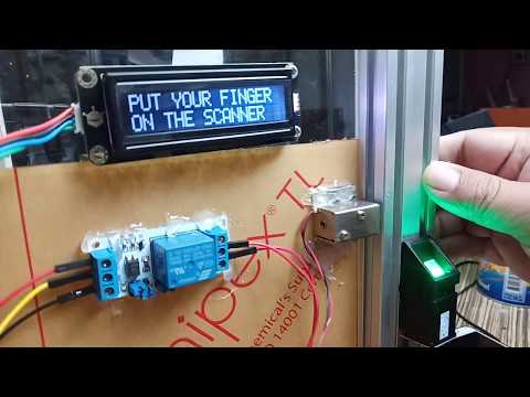
It is an obvious fact that each person has fingerprints. The fingerprints are actually the small ridges which are frictional in nature which makes it easier for a person to hold stuff. These fingerprints are being used for the security purpose because their pattern is unique for every individual. The fingerprints remains in its original shape forever, however in cases of severe accidents and burns it vanishes off. As a matter of fact, finger prints are unique for each individual and therefore through sensors its pattern can be acquired and used for making safe locks which are unbreakable. However, these locks are electronic in nature and requires a power bank or battery for its working. There is a small sensor on to which a specific finger is placed. The sensor is then detecting the fingerprint pattern and open up the lock if it matches the pattern saved in its memory, else it generates an alarm for false attempt.

Finger Prints PCBA

The Process of Enrollment and Verification of Fingerprints

Before the operation of the fingerprint locks you are required to put in the pattern of prints of the person who will be in charge of the security of a specific vicinity. The finger prints of the specific person are first saved in the memory of the lock.

The Process of Enrollment and Verification of Fingerprints

There are two processes for the purpose and each has its own importance. First stage is known as enrollment and the second stage is known as verification. The enrollment step is dealing with the system to learn the patterns of the specific person to be recognize. Some locks are supporting a single pattern while some are supporting more than one pattern recognition. Fingerprints of each person who would deal with the lock are scanned and analyzed and then saved in to the memory of the lock in a coded form which is unbreakable and secure as well. It takes a little time for the process of enrollment.

enrollment step Fingerprints pcba

The next step is verification when the lock is ready to be used. During this stage a person is attempting to open the closed lock. Now if the fingerprint on the sensor of the lock is authenticated, the lock will open up, however if not authenticated the lock will either generate alarm or will remain closed. Some locks are having specific number of attempts for wrong authentication. For instance, if a lock is having 3 attempts, then after 3 wrong authentication the lock will go in idle mode and will not be usable for some specific time encoded in its chip e.g. 1 hour etc.

verification PCBA

The Process of Storage and Comparison of Fingerprints

The fingerprints were only used in the criminal investigations in beginning, however gradually it came out to be best for using in security. When computer is checking the fingerprints, it does it by pattern recognition but not manually through a magnifying glass. The comparison among the fingerprints is made among the one which is already stored in the system or memory of the lock and the once which sensor has acquired from the person trying to unlock it. This is done through its comparison with feature known as minutiae which is taken at the time of enrollment and verification steps.

The fingerprints

The computer is basically measuring the distances as well as angles among the different prints of the finger through feature of minutiae. This all done through the help of a computer based algorithm known as unique numeric code. The uniqueness of the fingerprints is measured through comparison and the right pattern is detected and the access of the lock is granted.

The Working of Fingerprint Lock

You may have observed the phenomenon of taking fingerprints on a paper i.e. dipping finger in to an ink pad and then pressing it against paper for having its clear image. The prints are also stored in the computer in the same way but through sophisticated techniques. First of all the computer is scanning the entire surface area of the finger and converting in to a code. The sensor or scanner is an optical one which is working with a bright light taken through the finger and taking its photograph in digital format.

The Working of Fingerprint Lock

The process is somehow different from taking a simple photograph as it has a simple method of flashing through surface and taking its image. The sensor is catching the exact and required amount of the detail of the finger such as contrast and brightness. The ridges of the finger with all necessary details are precisely taken and then matched with one stored in database or memory of the lock. Quality control is one of the major factor of the fingerprint locks.

fingerprint locks

The following are major points.

  • 1- First of all the LEDs beneath the scanner are putting bright light on glass of scanner for taking clean picture of finger.
  • 2- Remember, some locks are taking more time for the capturing of picture for a bright and crisp image.
  • 3- An algorithm is testing the image taken from the sensor with one stored in database through pattern recognition algorithm.
  • 4- The algorithm is calculating the distances among ridges and then comparing with stored image.
  • 5- Once both images are matched then the lock is given autonomy to get open and access is granted for the person putting fingers on lock.
  • 6- In case of denial of the fingerprint, lock is either generating alarm or submerge to idle mode for a specific time and some locks have message service which sends a message to the owner of the vicinity for false attempt of access to lock.

Rayming provide Finger Print Locks design solution services including pcb manufacturing or prototoype pcb assembly services , you can get pcb assembly board Welcome to send mail to sales@raypcb.com , Get good price now !

How Many Common PCB Design Mistakes You Should Know

Altium PCB design process

The PCB designing work is not an easy task but it is an art that involves many aspects from routing, placement, component selection, holes and vias placement. The PCB designer can make mistake during the PCB design layout but that mistake or error can be identified by a interactive tool that is supported by many CAD software like ALTIUM. This integrated tool is known as Design Rule Checker (DRC)

YouTube video

Design Rule Checker (DRC):

The purpose of the DRC is to cross check the PCB layout design against the capabilities/constraints of PCB fabrication shop. These constraints are communicated in terms of maximum tolerances to the PCB layout design engineer and the design engineer simply input these values to the DRC checker and Run DRC. As a result, any discrepancy is identified and rectified. The common constraints that DRC run can check are trace width, hole to trace clearance, overlaps, drill size, keep out, angle, blind via ratio and many others.

Design For Manufacturing (DFM):

On the other hand, Design for Manufacturing (DFM) is a tool that can cover the grey areas that are left (remain unidentified) by DRC. This DFM (unlike DRC which is not an Ad-on but an integrated tool of CAD software) is an Ad-on provided for additional cost as an extra service by PCB fabricators to the customer. This can ultimately raise the cost of PCB because of DFM dedicated software is expensive and require manpower training. The DFM check will result in more qualified, reliable and high yield end product PCB.

Now we will discuss some common design issues that may not be caught in DRC checker run. These are

1. Starved thermal pads

Starved thermal pads

It is commonly observed that when reworking on a PCB during de-soldering the component from PCB, it takes lot of time, heat and effort. This is because the copper is a good conductor of heat. So when applying heat from soldering iron, the heat is wasted through the copper pour into the copper plane because the pad is completely surrounded by copper. So the component pad does not get enough heat to melt the solder and remove the electronic component.

This issue is resolved by soldering the component on thermal pad. Thermal pad can have 2 or 4 thermal relief traces that connect the pad to the copper pour to copper plane.  The air gap reduces the contact area so heat is not dissipated/wasted.

Now the design issue occurs when the thermal relief traces is not properly connected to copper pour or plane. The reason is the close proximity of multiple vias / pads or small spacing in between vias / pads. These small space may be cleared by DRC checker, but in actual the thermal relief traces will disturb the effected via and can displace vias from its copper pour.

 vias / pads

2. Acid Traps Acute Angle

During the PCB design process, the design engineer can unknowingly makes a mistake. This mistake is that the two traces meet/cross each other at โ€œacute anglesโ€ i.e less than 90O . As a result, the corners are made in the trace crossing point that can โ€œtrapโ€ acid inside it. The acid referred here is the PCB etching solution used to etch away unwanted/excess copper from the PCB and only useful copper is left for making tracks/traces. This acid / etching solution is commonly available Ferric Chloride or Hydrochloric Acid.

The โ€œacid trap holeโ€ is another similar thing that arises due to very less gap between the trace and via. This will cause the space or pockets to form and retain the acid inside.

These acid if trapped for long time, can eat away copper trace and hence creates open circuit that can render the PCB board defective. The possibility of acid traps in multilayer PCB is very high. Recent advancement in etching method (photo activated etching solution) of PCB has made this issue trivial but still best practice must be ensure to avoid acute angle traces.

Acid Traps Acute Angle

3. Copper Pour with Narrow Trace:

In some cases, like SOIC-08 IC package, the pad pitch is 5 mil and letโ€™s suppose the fabrication min spec is 10mil so it can short copper pour and pad as shown in the figure. In this figure the upper pour diagram shows the copper pour has width 0.005 inch while lower pour is 0.016 inch. And you can see that the lower pour is not present between the pads of SOIC. In Eagle Software this can be done by changing the copper pour width. This is the good practice as shown in lower pour and upper pour shown is a mistake that a PCB designer can make

If this mistake is made, this can result in breakage of this very thin 5 mil trace in little pieces which can float in other components of PCB to create short circuit.

Copper Pour with Narrow Trace:

4. Inadequate annular ring size

Inadequate annular ring size

The layers of PCB are interconnected by means of vias. The vias are made by drilling the holes on both sides and then plating the walls of holes thus interconnecting the inner layers and two external layers (sides) of PCB.

Now if the pad size is very small then the holes bored will take the large space on pad leaving very narrow or inadequate ring size. This is called annular ring. This insufficient annular ring is caused by inaccuracy in drill bit position and inaccuracy in hitting the target to drill holes .

annular ring

5. Via in Pads

Sometimes it is important for PCB designer to place a via in Pad of a component. This is done for sake of compact PCB routing. In traditional routing, DRC error can raise due to drill size and trace width etc. So for small pitch components like sub 0.5mm it is inevitable to use a via in Pad as shown in figure.

 Via in Pads

However the drawback of this is that this via will work as a straw that will suck the solder away from the pad and will cause the inadequate soldering of component upon the pad. The solution to this problem is to use โ€œCapped Viaโ€ as shown in this figure. Filling the conductive epoxy is also good.

Capped Via

6. Copper Layer near the board edge

The copper can be brought just close to the edge of PCB board because the design engineer does not include the โ€œkeep out layerโ€ or โ€œoutline layerโ€ in the Gerber Files. This keep out layer is very important because if it is not included then the copper can be exposed  to air and can cause trouble when boards are panelized resulting in short circuiting the copper layers. This feature can be easily caught in both DRC and DFM.

Copper Layer near the board edge

7. Missing solder mask between pads

Missing solder mask between pads

Solder mask is also called solder resist. It is used to protect the solder away from the copper track that you do not want to solder. For example in very small pitch components like QFN package 0.4mm pitch it is nearly impossible to apply solder mask in this tight space so it is common that you will not find solder mask because of standard DRC rules. This will result in a problem of solder bridge as shown in figure.

solder mask

8. Tombstoning

During the PCB assembly, when the small SMT passive components being soldered, the Tombstoning is caused by the improper wetting. When the solder paste starts to melt, an imbalanced torque at the ends of the component terminals causes the component to lift from one end.  The component will be lifted from the end where the paste is wet. This Tombstoning can damage the PCB yields and raise cost of production. Other factors that cause Tombstoning are

1- Improper design of solder pads

2- Uneven solder paste printing

3- Uneven temperature of reflow oven

4- Placement of component parallel to reflow oven conveyer

Tombstoning

From Virtual to Reality: How PCB Simulation Enhances Design Accuracy and Performance

PCB simulation has become an indispensable tool in electronics development, serving as the bridge between theoretical design and reliable production. By enabling comprehensive virtual testing, simulation empowers engineers to achieve unprecedented levels of precision while dramatically accelerating development cycles – two crucial factors in today’s competitive electronics industry.

Through advanced simulation techniques, designers can:

  • Identify and resolve potential signal integrity, power delivery, and thermal issues before prototyping
  • Optimize board performance while still in the digital design phase
  • Reduce physical prototyping iterations by up to 80%, according to industry studies
  • Ensure compliance with stringent EMI/EMC requirements

What is PCB Simulation?

PCB simulation is a process that involves creating a virtual model of a printed circuit board and its components to analyze and predict its behavior under various conditions. This powerful technique allows engineers to test and optimize their designs before physical prototyping, saving time, resources, and ensuring higher quality end products.

PCB simulation utilizes advanced software tools that incorporate complex mathematical models and algorithms to accurately represent the electrical, thermal, and mechanical properties of a PCB. By simulating real-world conditions, designers can identify potential issues, optimize performance, and validate their designs with a high degree of confidence.

The primary goal of PCB simulation is to bridge the gap between theoretical design and practical implementation. It provides a virtual environment where engineers can experiment with different design options, component placements, and circuit configurations without the need for physical prototypes. This approach not only accelerates the design process but also significantly reduces the risk of errors and costly revisions in later stages of product development.

Read more about:

Types of Simulations Used in PCB Design

PCB simulation encompasses various types of analyses, each focusing on different aspects of the board’s performance. Let’s explore the most common types of simulations used in PCB design:

1. Signal Integrity Simulation

Signal integrity (SI) simulation is a critical aspect of PCB design, especially for high-speed digital circuits. This type of simulation focuses on analyzing the quality and behavior of electrical signals as they travel through the PCB.

Key aspects of signal integrity simulation include:

  • Crosstalk analysis: Evaluating the interference between adjacent signal traces.
  • Impedance matching: Ensuring proper impedance control throughout the signal path.
  • Reflection analysis: Identifying and mitigating signal reflections that can cause distortions.
  • Timing analysis: Verifying signal timing and synchronization in complex designs.

By performing signal integrity simulations, designers can optimize trace routing, layer stackup, and component placement to maintain signal quality and minimize issues like electromagnetic interference (EMI) and signal distortion.

2. Thermal Simulation

As electronic devices become more compact and powerful, managing heat dissipation becomes increasingly critical. Thermal simulation allows engineers to predict and analyze the heat distribution across a PCB during operation.

Thermal simulation helps in:

  • Identifying hotspots: Locating areas of excessive heat generation on the board.
  • Optimizing component placement: Arranging components to ensure efficient heat dissipation.
  • Evaluating cooling solutions: Testing the effectiveness of heat sinks, fans, and other cooling mechanisms.
  • Predicting thermal stress: Analyzing the impact of temperature changes on board materials and components.

By conducting thermal simulations, designers can ensure that their PCBs operate within safe temperature ranges, preventing thermal-related failures and improving overall reliability.

3. Power Integrity Simulation

Power integrity (PI) simulation focuses on analyzing the power distribution network (PDN) of a PCB. This type of simulation is crucial for ensuring that all components receive stable and clean power supply throughout the board.

Power integrity simulation addresses:

  • Voltage drop analysis: Identifying areas where voltage levels may drop below acceptable thresholds.
  • Decoupling capacitor optimization: Determining the optimal placement and values of decoupling capacitors.
  • Current density analysis: Ensuring that traces and planes can handle the required current without overheating.
  • Resonance analysis: Identifying and mitigating potential resonance issues in the power distribution network.

By optimizing power integrity, designers can prevent issues like ground bounce, power supply noise, and electromagnetic interference, all of which can significantly impact the performance and reliability of the PCB.

4. Electromagnetic Compatibility (EMC) Simulation

Electromagnetic Compatibility (EMC) simulation is essential for ensuring that a PCB design complies with regulatory standards and operates correctly in its intended electromagnetic environment.

EMC simulation helps in:

  • EMI analysis: Predicting and mitigating electromagnetic interference generated by the PCB.
  • Susceptibility testing: Evaluating the board’s resistance to external electromagnetic disturbances.
  • Shielding effectiveness: Assessing the performance of EMI shielding techniques.
  • Antenna performance: Analyzing the behavior of intentional radiators like antennas in wireless devices.

By conducting EMC simulations, designers can identify potential compliance issues early in the design process, reducing the risk of failing regulatory tests and minimizing the need for costly redesigns.

Benefits of PCB Simulation

The adoption of PCB simulation in the design process offers numerous advantages that significantly impact the quality, efficiency, and cost-effectiveness of PCB production. Let’s explore these benefits in detail:

1. Cost Savings

One of the most significant advantages of PCB simulation is its ability to reduce overall development costs. By identifying and resolving issues in the virtual environment, designers can minimize the number of physical prototypes required. This reduction in prototyping iterations leads to:

  • Lower material costs: Fewer prototype boards and components need to be manufactured.
  • Reduced testing expenses: Less time and resources spent on physical testing of multiple iterations.
  • Minimized rework costs: Early detection of issues prevents expensive modifications in later stages.

2. Time Efficiency

PCB simulation dramatically accelerates the design process by allowing engineers to test and validate their designs quickly. This time-saving aspect manifests in several ways:

  • Rapid design iterations: Changes can be implemented and tested in minutes rather than days or weeks.
  • Parallel development: Different aspects of the design can be simulated simultaneously by team members.
  • Faster time-to-market: Reduced development cycles lead to quicker product launches.

3. Error Detection and Debugging

Simulation tools provide a comprehensive view of the PCB’s behavior, making it easier to identify and resolve potential issues:

  • Early problem detection: Issues are caught before physical prototyping, saving time and resources.
  • Root cause analysis: Simulation data helps in pinpointing the exact causes of problems.
  • Virtual troubleshooting: Designers can experiment with different solutions in a risk-free environment.

4. Performance Optimization

PCB simulation allows designers to fine-tune their designs for optimal performance:

  • Component optimization: Ideal component values and placements can be determined through simulation.
  • Layout refinement: Trace routing and layer stackup can be optimized for best signal integrity and EMC performance.
  • Power distribution optimization: Simulation helps in creating efficient and stable power delivery networks.

5. Reliability Improvement

By simulating various operating conditions and stress scenarios, designers can enhance the overall reliability of their PCBs:

  • Stress testing: Simulating extreme conditions helps in identifying potential failure points.
  • Longevity prediction: Thermal and power simulations can estimate the lifespan of components and the board.
  • Quality assurance: Comprehensive simulations reduce the likelihood of field failures.

6. Enhanced Collaboration

PCB simulation tools often come with collaboration features that improve team communication and productivity:

  • Shared simulation results: Team members can easily access and review simulation data.
  • Version control: Changes and improvements can be tracked and managed efficiently.
  • Remote collaboration: Simulation data can be shared and discussed across different locations.

7. Compliance Verification

Simulation helps in ensuring that PCB designs meet industry standards and regulatory requirements:

  • EMC compliance: EMC simulations help in meeting electromagnetic compatibility standards.
  • Safety standards: Thermal and power simulations assist in adhering to safety regulations.
  • Industry-specific requirements: Simulations can be tailored to meet specific industry standards (e.g., automotive, aerospace).

8. 3D Visualization and Analysis

Modern PCB simulation tools offer powerful 3D visualization capabilities:

  • Spatial analysis: Designers can evaluate component placement and board layout in three dimensions.
  • Interference checking: 3D models help in identifying potential mechanical conflicts.
  • Aesthetic considerations: Visual representation aids in designing visually appealing products.

9. Improved Decision-Making

Simulation data provides a solid foundation for making informed design decisions:

  • Data-driven choices: Decisions are based on quantitative simulation results rather than guesswork.
  • Trade-off analysis: Designers can evaluate the impact of different design choices on overall performance.
  • Risk assessment: Potential issues can be quantified and prioritized based on simulation outcomes.

10. Integration with Manufacturing Processes

PCB simulation can be integrated with manufacturing processes to ensure smoother production:

  • DFM (Design for Manufacturing) optimization: Simulation helps in creating designs that are easier to manufacture.
  • Yield improvement: By identifying potential manufacturing issues early, designers can improve production yield.
  • Process simulation: Some tools allow simulation of manufacturing processes to predict and prevent production issues.

How to Simulate a PCB Design

Simulating a PCB design involves several steps and requires the use of specialized software tools. Here’s a general overview of the process:

1. Prepare the Design Data

Before simulation can begin, you need to have a complete PCB design, including:

2. Choose the Appropriate Simulation Type

Based on your design goals and concerns, select the type of simulation you want to perform:

  • Signal integrity
  • Power integrity
  • Thermal analysis
  • EMC simulation

3. Set Up the Simulation Environment

Configure the simulation software with the necessary parameters:

  • Import your PCB design data
  • Define simulation boundaries and conditions
  • Set up excitation sources and loads
  • Specify frequency ranges or time domains for analysis

4. Run the Simulation

Execute the simulation and wait for the results. Depending on the complexity of your design and the type of simulation, this process can take anywhere from a few minutes to several hours.

5. Analyze the Results

Once the simulation is complete, carefully examine the output data:

  • Review waveforms, graphs, and 3D visualizations
  • Look for any violations of design rules or performance thresholds
  • Identify areas that require optimization or further investigation

6. Iterate and Optimize

Based on the simulation results:

  • Make necessary changes to your design
  • Re-run simulations to verify improvements
  • Repeat the process until desired performance is achieved

7. Document and Report

Create comprehensive reports documenting the simulation process, results, and any design changes made. This documentation is valuable for team collaboration, design reviews, and future reference.

Can I Do PCB Simulation Online?

Yes, it is possible to perform PCB simulation online through various cloud-based platforms and services. Online PCB simulation offers several advantages:

  • Accessibility: You can access simulation tools from any device with an internet connection.
  • Reduced hardware requirements: Heavy computations are performed on remote servers, reducing the need for powerful local hardware.
  • Automatic updates: Cloud-based tools are typically updated automatically, ensuring you always have the latest features and models.
  • Collaboration: Online platforms often provide better tools for team collaboration and sharing of results.

However, there are also some considerations to keep in mind:

  • Internet dependency: A stable internet connection is crucial for uninterrupted simulation.
  • Data security: Ensure that the online platform you choose has adequate security measures to protect your design data.
  • Subscription costs: Many online simulation tools require ongoing subscription fees.
  • Limited customization: Some online tools may offer fewer customization options compared to traditional desktop software.

Some popular online PCB simulation platforms include:

  1. Altium 365
  2. EDA Board
  3. CircuitMaker
  4. PCBWeb
  5. Upverter

When choosing an online PCB simulation tool, consider factors such as the types of simulations offered, ease of use, integration with your existing design workflow, and pricing structure.

Best 5 PCB Simulation Software

While there are numerous PCB simulation tools available in the market, some stand out for their comprehensive features, accuracy, and user-friendliness. Here are five of the best PCB simulation software options:

1. ANSYS SIwave

ANSYS SIwave is a powerful electromagnetic simulation tool specifically designed for PCB and IC package analysis. It excels in:

  • Signal integrity analysis
  • Power integrity simulation
  • EMI/EMC prediction
  • 3D full-wave electromagnetic field solving

Pros:

  • Highly accurate simulations
  • Seamless integration with other ANSYS tools
  • Supports complex, multi-layer designs

Cons:

  • Steep learning curve
  • Relatively high cost

2. Cadence Sigrity

Cadence Sigrity offers a suite of analysis tools for PCB and IC package design, including:

  • Signal integrity analysis
  • Power integrity simulation
  • Thermal analysis
  • EMI/EMC simulation

Pros:

  • Comprehensive simulation capabilities
  • Good integration with Cadence PCB design tools
  • Supports advanced technologies like DDR4 and PCIe

Cons:

  • Can be resource-intensive for complex simulations
  • Requires significant expertise for optimal use

3. Keysight ADS (Advanced Design System)

Keysight ADS is a comprehensive electronic design automation software that includes powerful PCB simulation capabilities:

  • EM simulation
  • Signal integrity analysis
  • Power integrity simulation
  • Thermal analysis

Pros:

  • Wide range of simulation types in one package
  • Excellent for RF and microwave designs
  • Strong support for high-speed digital design

Cons:

  • Complex user interface
  • High initial learning curve

4. Mentor HyperLynx

Mentor HyperLynx, now part of Siemens Digital Industries Software, offers a suite of easy-to-use yet powerful PCB simulation tools:

  • Signal integrity analysis
  • Power integrity simulation
  • EMC analysis
  • Thermal simulation

Pros:

  • User-friendly interface
  • Fast simulation times
  • Good balance of ease-of-use and advanced features

Cons:

  • May lack some advanced features found in more specialized tools
  • Limited customization options for some analyses

5. PADS Professional

PADS Professional, also part of the Mentor Graphics (Siemens) family, provides integrated PCB design and analysis capabilities:

  • Signal integrity simulation
  • Power integrity analysis
  • Thermal analysis
  • EMI/EMC simulation

Pros:

  • Integrated design and simulation environment
  • Scalable solution suitable for individual engineers to large teams
  • Good price-to-performance ratio

Cons:

  • Some advanced features may require additional modules
  • Less specialized than some dedicated simulation tools

When choosing PCB simulation software, consider factors such as:

  • Types of simulations required for your designs
  • Integration with your existing PCB design tools
  • Available computing resources
  • Budget constraints
  • Team expertise and training requirements

It’s often beneficial to trial multiple software options to find the one that best fits your specific needs and workflow.

The Traditional PCB Design Process vs. a Process Integrated with Simulation

The integration of simulation into the PCB design process has significantly transformed the way electronic products are developed. Let’s compare the traditional PCB design process with a modern approach that incorporates simulation at various stages:

Traditional PCB Design Process

  1. Conceptualization: Define product requirements and create initial schematics.
  2. Schematic Design: Develop detailed circuit schematics.
  3. Component Selection: Choose appropriate components based on specifications.
  4. PCB Layout: Create the physical layout of the board.
  5. Design Rule Check (DRC): Verify that the layout meets basic design rules.
  6. Prototype Manufacturing: Produce a physical prototype of the PCB.
  7. Testing and Debugging: Physically test the prototype and identify issues.
  8. Revisions: Make necessary changes based on test results.
  9. Final Production: Once satisfactory results are achieved, move to full production.

PCB Design Process Integrated with Simulation

  1. Conceptualization: Define product requirements and create initial schematics.
  2. Schematic Design: Develop detailed circuit schematics.
  3. Initial Simulation: Perform basic simulations to verify circuit behavior.
  4. Component Selection: Choose components based on simulation results and specifications.
  5. PCB Layout: Create the physical layout of the board.
  6. Comprehensive Simulation:
    • Signal integrity simulation
    • Power integrity simulation
    • Thermal analysis
    • EMC simulation
  7. Design Optimization: Refine the design based on simulation results.
  8. Design Rule Check (DRC): Verify that the layout meets design rules and simulation-derived constraints.
  9. Virtual Prototyping: Create and analyze a complete virtual model of the PCB.
  10. Design Review: Conduct a thorough review based on simulation results and virtual prototype performance.
  11. Physical Prototype Manufacturing: Produce a physical prototype with high confidence in its performance.
  12. Validation Testing: Conduct physical tests to confirm simulation predictions and overall performance.
  13. Final Adjustments: Make minor tweaks if necessary, based on validation results.
  14. Production: Move to full-scale production with a highly optimized and verified design.

Key Differences and Advantages of Simulation-Integrated Process

  1. Early Problem Detection: Simulation allows issues to be identified and resolved much earlier in the design cycle, reducing costly late-stage changes.
  2. Reduced Prototyping Iterations: By catching and fixing issues virtually, fewer physical prototypes are needed, saving time and resources.
  3. Optimized Designs: Simulation enables designers to fine-tune their designs for optimal performance before physical production.
  4. Increased Confidence: Engineers have a much higher level of confidence in their designs before moving to production.
  5. Faster Time-to-Market: The overall design process can be significantly accelerated by reducing physical prototyping and testing cycles.
  6. Cost Efficiency: While there may be an initial investment in simulation tools, the long-term savings in prototyping and redesign costs are substantial.
  7. Enhanced Collaboration: Simulation results provide concrete data for team discussions and decision-making.
  8. Improved Documentation: Simulation processes and results contribute to more comprehensive design documentation.

By integrating simulation throughout the PCB design process, engineers can create more reliable, high-performance designs while saving time and resources.

Difference Between PCB Simulation and Reality Boards

While PCB simulation has become an indispensable tool in the design process, it’s important to understand its relationship with physical, real-world boards. Let’s explore the key differences and considerations:

1. Idealized vs. Real-World Conditions

  • Simulation: Uses idealized models and controlled conditions. Can simulate perfect scenarios that may not exist in reality.
  • Reality: Subject to real-world variations, imperfections, and environmental factors not always accounted for in simulations.

2. Component Tolerances

  • Simulation: Often uses nominal values for components, though advanced simulations can incorporate tolerance ranges.
  • Reality: Actual components have manufacturing tolerances that can affect circuit behavior.

3. Environmental Factors

  • Simulation: Can model specific environmental conditions, but may not capture all real-world variables.
  • Reality: Exposed to varying temperatures, humidity, electromagnetic interference, and other environmental factors.

4. Manufacturing Variations

  • Simulation: Typically assumes perfect manufacturing processes.
  • Reality: Subject to variations in PCB fabrication, such as etching tolerances, material inconsistencies, etc.

5. Aging and Wear

  • Simulation: Generally models new components and materials.
  • Reality: Components and materials degrade over time, affecting long-term performance.

6. Unexpected Interactions

  • Simulation: Based on known models and interactions.
  • Reality: May exhibit unexpected behaviors due to unforeseen interactions between components or external factors.

7. Simulation Accuracy vs. Computation Time

  • Simulation: More accurate simulations often require longer computation times, leading to trade-offs between accuracy and speed.
  • Reality: Real-world performance is instantaneous but may require extensive testing to fully characterize.

8. Cost and Time Investment

  • Simulation: Requires upfront investment in software and training but allows for rapid iterations.
  • Reality: Physical prototyping can be more expensive and time-consuming but provides definitive real-world results.

Bridging the Gap

To maximize the benefits of simulation while ensuring real-world performance, consider the following approaches:

  1. Correlation Studies: Regularly compare simulation results with measurements from physical prototypes to improve simulation accuracy.
  2. Design Margins: Include safety margins in designs to account for real-world variations not captured in simulations.
  3. Statistical Analysis: Use Monte Carlo simulations to account for component tolerances and manufacturing variations.
  4. Hybrid Approach: Combine simulation with targeted physical testing for critical aspects of the design.
  5. Continuous Learning: Use discrepancies between simulated and real results to refine simulation models and techniques.
  6. Advanced Modeling: Incorporate more sophisticated models that account for non-ideal behaviors, parasitics, and environmental factors.
  7. Post-Production Validation: Conduct thorough testing on production boards to verify that real-world performance aligns with simulation predictions.

Conclusion

PCB simulation has revolutionized the electronic design process, offering numerous benefits including cost savings, time efficiency, and performance optimization. By bridging the gap between virtual designs and physical realities, simulation tools enable engineers to create more reliable, high-performance PCBs with greater confidence.

While differences between simulated and real-world results will always exist, the continuous advancement of simulation technologies is narrowing this gap. By understanding the strengths and limitations of PCB simulation, designers can leverage these powerful tools effectively, complementing them with appropriate physical testing and validation.

As the complexity of electronic designs continues to increase, the role of PCB simulation in ensuring product quality, reliability, and time-to-market advantages will only grow. Embracing and mastering these simulation techniques is crucial for staying competitive in the rapidly evolving field of electronic design.

By integrating PCB simulation into their workflow, designers and engineers can push the boundaries of what’s possible in electronic design, creating innovative products that meet the demanding requirements of today’s technology-driven world.

What is DFM Check?

design for manufacturing

Introduction

DFM stands for Design for Manufacturing. DFM check is the process of analyzing a product design to ensure it can be manufactured efficiently and cost-effectively.

With DFM analysis, engineers examine the design to identify and correct issues before releasing it to production. This avoids costly manufacturing problems down the line.

In this comprehensive guide, we will cover:

  • The importance of DFM analysis
  • When DFM checks should be performed
  • The major areas analyzed in a DFM check
    • Tolerances
    • Clearances
    • Draft angles
    • Surface finishes
    • and more
  • DFM principles and guidelines
  • Performing manual vs automated DFM checks
  • Fixing DFM violations
  • FAQs

By the end of this article, you will have a strong understanding of what DFM analysis entails and how it improves manufacturability. Let’s get started!

The Importance of DFM Analysis

PCB DFM

DFM analysis provides enormous benefits for manufacturing by optimizing the design early on. Here are some key reasons DFM checks are critical:

  • Saves money – It is far cheaper to fix issues in design stage rather than after production starts. DFM optimizes costs.
  • Prevents defects – Flaws from a problematic design get replicated in every manufactured unit. DFM catches problems before they occur at scale.
  • Avoids delays – A faulty design necessitates reworks and retrofits, stalling production. DFM prevents this wasted time.
  • Improves quality – DFM facilitates higher assembly success, fewer scrapped parts, and consistent quality.
  • Increases manufacturability – The design gets tailored to the capabilities of the manufacturing process.

For these reasons, leading engineering teams perform extensive DFM checks before releasing any product to the factory floor. The ROI from avoiding manufacturing issues is tremendous.

When Should DFM Analysis Be Performed?

DFM checks should be performed at multiple stages of the design process:

  • Conceptual design phase – Early DFM analysis ensures the design direction inherently accounts for manufacturing best practices.
  • Detailed design phase – Rigorous DFM checks should be conducted once the detailed design is frozen before release to production.
  • Design revisions – DFM checks also needed whenever design changes are made to ensure no new issues are introduced.

In general, DFM checks should be an ongoing process throughout development rather than a one-time step at the end. Issues caught early in design iterations can prevent costly changes later down the line.

For complex products, DFM checks may be performed by a dedicated manufacturability engineering team. They take the designer’s CAD model and run intensive DFM analysis on it as a service.

No matter the design phase, integrating DFM as early and often as possible is key for optimizing manufacturability.

Major Areas Analyzed in a DFM Check

DFM analysis involves assessing the design from multiple aspects that impact manufacturing. Here are some of the major areas checked in a DFM review:

Tolerances

  • Tolerance stackups calculated to ensure parts will fit together within specified range
  • Tolerances not too tight for process capabilities
  • Statistical tolerance analysis conducted where possible

Clearances

  • Sufficient clearances between components for material thickness
  • Adequate clearances to access assemblies and fasteners
  • Clearances checked for operation without interference
  • Minimum electrical clearances met

Draft Angles

  • Draft angles added on vertical faces to ease ejection from molds
  • Uniform draft angle between adjacent faces
  • Adequate draft for deep/high parts and materials used

Hole Sizes

  • Hole diameters meet tap drill sizes for specified thread types
  • Hole sizes account for plating tolerances if plated
  • Large holes have web thicknesses for required strength

Surface Finishes

  • Appropriate surface finish specs for functional needs
  • Finishes avoid tight textures causing friction or galling
  • Radius surface finishes specified where needed

Heat Sinks

  • Heat sinks sized properly for heat load and air flow
  • Thermal interface material thickness considered
  • Fins aligned with air flow direction

Welds

  • Weld types appropriate for materials and joint design
  • Gaps provided for welding access
  • Distortion from weld process and sequencing minimized

Part Symmetry

  • Parts designed symmetric where possible to avoid orientation concerns
  • Non-symmetric parts clearly identified in drawings

Stamping and Forming

  • Draw depths and minimum radii suitable for material thickness
  • Bend radiuses checked for sheet metal parts
  • Stamping web widths adequate for strength

Molding

  • Draft angles provided on molded parts
  • Radii added to corners to ease fill
  • Core pins accessible and adequate for details
  • Undercuts eliminated unless using collapsible cores

Casting

  • Casting draft present with proper direction
  • Minimum thicknesses to avoid porosity observed
  • Appropriate finish allowances specified

Fastening and Joining

  • Fastener sizes appropriate for materials and assemblies
  • Fastener spacings meet engineering requirements
  • Adhesives and press fits designed for required strength

Part Handling

  • Points identified for safe automated part handling
  • Low friction surfaces checked where automated sliding occurs
  • Weight limits observed for manual lifting and ergonomics

Assembly Sequence

  • Efficient tabs snap features used where helpful
  • Conditional assembly sequences enabled where needed
  • Assembly performed from stable datum points first

Test and Inspection

  • Test points provided to verify full assembly
  • Key dimensions defined for in-process inspection
  • Go/no-go assembly checks incorporated

This covers some of the major areas scrutinized during a thorough DFM analysis. The full scope depends on the specific design and manufacturing process.

Key DFM Principles and Guidelines

While checking the above details, DFM engineers are guided by fundamental DFM principles that influence the overall manufacturability of a design:

Simple and Intuitive

  • Design should be as simple as possible while still meeting functional needs
  • Avoid unnecessary complex geometries and mechanisms
  • Intuitive assemblies are easier to manufacture correctly

Error Proofing

  • Incorporate go/no-go checks to prevent incorrect assembly
  • Include guides, keys, and asymmetry for foolproof assembly
  • Eliminate ways to assemble incorrectly through smart design

Standardization

  • Maximize use of standard parts, materials, processes
  • Follow industry and in-house standards where possible

Process Capabilities

  • Stay within known process capabilities -avoid pushing limits
  • Account for inherent process variation in tolerances

Modularity

  • Break complex designs into self-contained modules
  • Standard interfaces between modules for flexibility
  • Modules can be made and tested independently

Consolidation

  • Combine parts into single parts where possible
  • Avoid unnecessary joints/fasteners to consolidate

Handling

  • Design parts to be easily handled and positioned
  • Add fiducials and other features to assist automation

Service and Repair

  • Enable access to lifecycle maintainable components
  • Fasteners, connectors, etc. designed for serviceability

By adhering to DFM principles like these, engineers can design products with manufacturing in mind right from the start. This flows into all the detailed checks conducted later.

Performing Manual vs Automated DFM Checks

DFM analysis is traditionally conducted manually by experienced engineers trained in manufacturing processes. However, automated DFM checking software has also emerged to supplement manual review.

Manual DFM Checking

With manual DFM analysis, engineers use their expertise to:

  • Visually inspect CAD models for issues using a checklist
  • Calculate key dimensions, stacks, and clearances by hand
  • Simulate assembly sequences to validate manufacturability
  • Judge surface finishes, drafts, radiuses by sight
  • Suggest design changes to fix found issues

Manual checking taps into an engineer’s manufacturing knowledge. But it can be tedious and prone to human error.

Automated DFM Checking

DFM software automatically checks models for common issues like:

  • Insufficient draft angles on faces
  • Tight component clearances
  • Hole dimensioning errors
  • Thickness and radius violations
  • Interference detection
  • Standard violation checking

Automated tools provide consistent, rapid analysis. But software cannot fully replace an engineer’s judgement and insight yet.

In practice, the two methods are combined – engineers first run an automated DFM analysis then manually review the flagged issues. This gives the best results.

Fixing DFM Violations

When issues are identified from DFM checks, the designer needs to modify the CAD model to address them. Here are typical ways DFM violations are fixed:

  • Relaxing tolerances – Increase tolerance windows to viable ranges
  • Changing dimensions – Resize parts and geometry to meet requirements
  • Adding draft – Add or increase draft angles where lacking
  • Altering surface finishes – Change surface specs to better finishes
  • Revising hole features – Modify hole sizes to suit tap sizes or add webbing
  • Adding clearance – Provide adequate clearance between components
  • Eliminating undercuts – Remove undercuts in molded parts through design changes
  • Changing joinery – Revise joints, fasteners to improve assemble-ability
  • Simplifying geometry – Simplify complex shapes to the basic functional geometry
  • Separating parts – Break convoluted parts into simpler individual parts
  • Refining assembly sequence – Optimize assembly steps for efficiency and clarity

Usually, many small changes are required versus one major redesign. The designer iterates to incrementally improve the design based on the DFM feedback.

Frequently Asked Questions

Here are some common questions that arise regarding DFM analysis:

Q: When should DFM analysis be done – by designers or by manufacturing engineers?

A: DFM principles should first be applied during the initial design phase. Later extensive DFM checks can be done by manufacturing engineers as an independent quality check.

Q: What are some limitations of automated DFM analysis tools?

A: Automated tools miss context-specific issues and have limited capability to suggest fixes. But they rapidly find basic issues like insufficient drafts.

Q: How is DFM analysis different for machined parts versus plastic injection molded components?

A: Each process has unique DFM considerations – for machining, avoid thin walls, deep pockets, and surfaces hard to reach with cutters. For molding, check drafts, radii, tolerances.

Q: What is the right level of detail for a DFM analysis?

A: It depends on the design complexity, production volume, cost, lead time, and other factors. Higher volume or cost products warrant extremely exhaustive DFM review.

Q: Is DFM analysis applicable beyond mechanical and physical product design?

A: Yes, the principles of optimizing a design for ease of execution extend to many fields. DFM concepts are relevant even in UX design, process design, and more.

Conclusion

DFM analysis is a critical step in optimizing a product design for manufacturing and assembly. By thoroughly checking key areas like tolerances, clearances, surface finishes, and reviewing the design from a manufacturing perspective, engineers can catch and correct issues early.

Performing DFM checks systematically at each stage of design, incorporating both automated tools and manual review by experienced engineers, results in the highest quality analysis. The ROI from avoiding manufacturing problems is well worth the effort invested into rigorous DFM practices.

With the methodology and best practices covered in this guide, you now have strong knowledge of what an effective DFM analysis entails. Leverage DFM practices in your organization to save costs, reduce defects, shorten time-to-market, and ultimately create products optimized for manufacture.

Free of Cost DFM Check

DFM (Design for Manufacturing ) is known as file check and it is basically an added value service that most of PCB manufacturers offer. The services of DFM are related to the checking of PCB design for any possibility of issues which may hinder the process of PCB manufacturing and fabrication. In case if any issues are sorted, customers are got in touch on immediate basis and issues are resolved at higher priority and fabrication of PCBs is arranged accordingly.

YouTube video

The DFM check offered by RayPCB is cost-effective of the system we use for DFM check is an autonomous way for enabling the manufacturing and fabrication system of PCBs hassle-free and sort out issues which cause trouble. The autonomous system of FDA check is known as Valor DFM. The system helps in lowering cost of PCB and saves time as well. The DFM is conducted on the basis of five aspects at RayPCB known as single layer and mixed layer checks, silkscreen checks, drill checks, and ground/power checks. The details are given below.

1. Drill Checks:

The action of drill checks is for finding out the potential defects which may hinder the manufacturing process in different layers of PCB. Statistics are generated on drill layers. The drill checks is supposed to be operated on drill layers only. It is using drill stack, bottom and top layers along with ground or power layer in stack. The checklists are given below.

ItemsFunctionalities
Ground/Power ShortsIt reports the drills which are touching copper nets of more than ground or power layer.
NPTH to RouteIt reports the drills which are having mounting or tool hole and NPTHs which are very close to path.
Missing HolesIt reports the holes which are missing drills.
Hole SizeIt offers list of vias, NPTHs, and PTHs which required drills.
Extra HolesIt reports the extra holes which are redundant and are not belonging to any of the Pads.
Hole separationIt reports the extra holes or duplicate holes or the holes which are closed.
Thermal ConnectionIt reports the absence of thermals for pin drills and calculates the approximated copper area for each thermal connection via mixed and ground layers.
Stubbed ViasIt reports the vias which are not connected to two or more copper layers.
Drill Checks

2. Mixed and Single Layered Checks:

The mixed and single layered checks is designed for finding potential manufacturing defects and generation of statistics in mixed and single layers. The action is dedicated for single layers, however it can also be implemented on mixed and other layers. The main checklist are given below.

ItemsFunctionalities
SizeIt has information of the size of pads, text, arcs, line neck downs, vias, shaved arcs, and shaved lines.
StubsIt has information of endpoints of unconnected lines.
SpacingIt has information of the violations among nets and circuits of pads among text, shorts, and spacing among CAD nets and non-touching features of CAD.
SilverIt has information of the silver lines among pads and lines.
RouteIt has reports of the displacement violations among pads and edge of route.
DrillIt has information of the displacement among vias, NPTHs, PTHs, Pads, rings, Circuits, and copper etc.

3. The Ground/Power Checks:

The intentions of the ground/power checks is to have an identification of the manufacturing defects in ground and power in mixed layers. It has utilization of various algorithms for diagnosis of positive and negative power along with ground layer. Checklist is given as follow.

ItemsFunctionalities
RouteIt has report of the closed spacing among route and copper features.
NFP SpacingIt has information of spacing among NFP-planes, and NFP-NFP.
DrillIt has information of distance violations among vias to plane, annular rings, clearance, and copper etc.
Plane SpacingIt has information of spacing among various features of planes.
ThermalIt has information of spoke reduction and width of the connectivity of thermal pads.
Plane WidthIt has reports of inadequate width of the layer of copper among 2 drills which are connected on copper plane.
Keepout AreasIt has information of features of outside and inside as well as keepout and keepin areas.
Plane ConnectionIt has reporting of the detached areas of copper which are utilized as reference planes and are in design which are causing unreferenced net or missing electrical connection.
The Ground/Power Checks

4. The Solder Mask Checks:

This function is for checking layers of solder masks for any potential manufacturing defects. The layers of solder masks are considered negative and the positive features are describing clearance of the solder masks. The function is also checking the solder paste which is deposited on the pads. This function is operating on single layer solder mask and below is its major checklist.

ItemsFunctionalities
SpacingIt has information of the spacing among clearance.
ExtraIt has a reporting of soldering mask features which are lacking copper pads and are not intersecting each other.
DrillIt has reporting of close distant to solder mask opening of NPTH annular rings.
BridgeIt has information of pads which are there without solder mask.
SilverIt has reports of the silvers among clearance and solder mask.
MissingIt has reports of the missing clearances.
CoverageIt has information of lines which are too close to clearance.
PadsIt has reports of the opening of distance to solder mask of pads comprising of undrilled pads. It has information of special group as well such as gaskets, information of width of solder mask etc.

5. The Silkscreen Checks:

This function has an intention of finding potential manufacturing defects present in layers of silkscreen and also generation of statistics. This function is only used for checking silk screen layers because it has a reliance on job matrix related to external copper, layers of drills and solder mask. Below are details of checklist.

ItemsFunctionalities
String OverlapIt has information of intersection or touching of silkscreen with various string values.
SMD ClearanceIt has information about spacing among SMD pads and silkscreen features.
Pad ClearanceIt has reports of spacing among pads and silkscreen features.
Solder Mask ClearanceIt has information of spacing among clearance of solder mask and silkscreen features.
Hole ClearanceIt has information of spacing among drills and silkscreen features.
Line WidthIt has information of the violations of width and length to its respective ratio.
Route ClearanceIt has information of spacing among route features and silkscreen features.

You can avail advantage of DFM free check offered by RayPCB right away. Donโ€™t waste time and contact us right now for availing this amazing deal of free DFM check.

More PCB Design guides :

kicad 6 kicad 7 Download and Tutorial

Kicad PCB

Introduction

KiCad is a free, open source electronic design automation (EDA) software suite used for printed circuit board (PCB) design. It features schematic capture, PCB layout, gerber file generation, and much more. KiCad supports Windows, macOS, and Linux operating systems.

In this comprehensive tutorial, we will cover:

  • A brief history of KiCad
  • Key features of KiCad
  • Downloading and installing KiCad
  • Creating a schematic and PCB in KiCad
    • Adding components
    • Connecting components and wiring
    • Designing the board outline and layers
    • Generating gerber and drill files
  • Tips and tricks for using KiCad effectively
  • FAQs

By the end of this tutorial, you’ll have a solid understanding of how to use KiCad 6 and 7 for all your PCB design needs. Let’s get started!

A Brief History of KiCad

KiCad schematic tutorial

KiCad was started in 1992 by Jean-Pierre Charras as a personal project while working at IUT Cachan electrical engineering department. The first versions of KiCad focused solely on board layout and routing.

Over the years, KiCad continued gaining new features like schematic capture, Gerber file output, and more. Jean-Pierre led the development until 2013 when the KiCad project entered a long maintenance period.

In 2015, CERN sponsored KiCad developers to add advanced features like hierarchical schematics and improve documentation. This led to the major KiCad 4.0 release in 2015.

KiCad continued improving with versions 5.0 and 5.1 released in 2017 and 2019. The latest releases are KiCad 6.0 in 2021 and KiCad 7.0 in 2022 with huge advancements like push and shove routing, differential pair routing, and more.

Today, KiCad has a thriving open source community with contributors worldwide. It has become one of the most popular EDA tools for hobbyists and professionals alike.

Key Features of KiCad

Here are some of the standout features that make KiCad a great choice for PCB design:

  • Cross-platform – KiCad runs natively on Windows, macOS, and Linux. Project files are compatible across platforms.
  • Hierarchical schematics – Large, complex schematics can be broken down into reusable sheets and blocks to simplify design.
  • Customizable layout – The PCB editor is highly configurable. Users can customize keyboard shortcuts, snap grids, trace widths, and more.
  • Advanced PCB editing – KiCad includes features like push and shove routing, differential pair routing, and length tuning to simplify board routing.
  • 3D visualization – PCBs can be viewed and inspected in 3D with renderings of components and pins. Great for design verification.
  • Flexible manufacturing outputs – KiCad can generate Gerber and drill files, schematic PDFs, BOMs, 3D models, and more.
  • Free and open source – KiCad is licensed under an open source GNU GPL v3 license. Users can access the source code to tweak and extend KiCad’s functionality.
  • Large component library – A huge library of schematic symbols and 3D models for common components. Users can also create custom components.
  • CLI tools – Command line tools are included for advanced tasks like scripting repetitive operations.
  • Customizable footprints – Footprint editor lets users create and modify component footprints to match datasheets.

With these features and many more, KiCad provides everything needed for professional PCB design. It’s no wonder KiCad has become so popular worldwide.

Downloading and Installing KiCad

KiCad is available for Windows, macOS, and Linux operating systems. Here are the steps to download and install KiCad:

Windows Installation

  1. Go to kicad.org and download the Windows installer under “Software Download”.
  2. Run the installer .exe file and follow the installation wizard. This will install KiCad and all its associated tools.
  3. The default installation options are fine for most users. Make sure to install the 3D models library for PCB visualization.
  4. Once installation completes, KiCad will be available from the Windows start menu.

macOS Installation

  1. Go to kicad.org and download the macOS .dmg file under “Software Download”.
  2. Double click the .dmg file to open it, then drag the KiCad app icon into your Applications folder to install.
  3. Optionally, install the 3D models library for PCB visualization. This is available as a separate download.
  4. Launch KiCad from your Applications folder. It’s now installed and ready to use!

Linux Installation

KiCad is available in the package repositories for most Linux distributions like Ubuntu, Fedora, Arch, etc. It can be installed via the distribution’s package manager.

For example, on Ubuntu:

Copy code

sudo apt update sudo apt install kicad kicad-libraries kicad-footprints

On Fedora:

Copy code

sudo dnf install kicad kicad-libraries kicad-footprints

The kicad-libraries and kicad-footprints packages contain component symbols and footprints for KiCad.

That covers the basics of downloading and installing KiCad on the major operating systems. With KiCad installed, you are ready to start creating designs.

Creating a Schematic in KiCad

EasyEda to KiCad

The first step in any KiCad project is creating the schematic diagram. This represents the circuit connections between components. Here is a walkthrough of creating a simple schematic with KiCad:

  1. Launch KiCad and click File > New Project > New Project to start a new project.
  2. Enter a project name and file location to save the project. The default options are fine. Click OK.
  3. In the “Project specific properties” dialog, make any changes to the default design settings. For now we’ll use the defaults. Click OK.
  4. The KiCad main window will open with two tabs – Schematic and PCB Layout. Click the Schematic tab.
  5. In the schematic editor toolbar, click the “Add component” icon. This opens the component selector.
  6. Search for components you want to add, like resistors, capacitors, microcontrollers etc. Select a component and click OK to add it.
  7. Continue adding all needed components to the schematic. Press ‘R’ while hovering over a component to rotate it.
  8. To connect components, click the “Wire” tool to draw connection lines between component pins.
  9. Add power symbols from the component bar and connect them to pins as needed.
  10. Once the schematic is complete, click the PCB Layout tab to advance to the board layout stage.

This outlines the basics of creating a schematic in KiCad – adding components from the libraries, wiring them together, and connecting power. With the schematic ready, we can now layout the PCB.

Creating a PCB Layout in KiCad

After finishing the schematic, the next step is laying out the board outline, footprints, and routing copper traces between footprints. Here is an overview of designing a PCB layout with KiCad:

  1. In the PCB editor toolbar, change the layer to “Edge.Cuts” using the layer dropdown.
  2. Select the Add Graphic Line or Rectangle tool. Draw a rectangular or polygonal outline for the board perimeter.
  3. Switch to the F.Cu layer. This is the top copper layer for PCB traces.
  4. Using the Add Footprint tool, select footprints from the library and place them on the board. Arrange them sensibly.
  5. Inspect the Ratsnest lines. These show connections that need to be routed on the PCB.
  6. Begin routing traces between pins by selecting the Route Tracks tool. Click from pin to pin to complete each trace.
  7. For routed traces, click a completed track to add corner vias to other layers when needed.
  8. Use the Push and Shove router for difficult traces by selecting Route > Auto > Push and Shove Router.
  9. Complete routing all required electrical connections between components.
  10. Use the Design Rules Check to validate the PCB design meets specified electrical and clearance constraints.

With the board outline defined, footprints placed and traces routed, the PCB layout is now complete! We can now generate manufacturing output files.

Generating Manufacturing Output Files

The last step is generating Gerber and drill files needed to manufacture the designed PCB. Here are the steps to generate outputs with KiCad:

  1. With the PCB layout open, click File > Fabrication Outputs > Gerber Files.
  2. Select the layers needed for manufacturing. Most PCB fab houses will want copper layers, soldermask, legend, etc.
  3. Click the “Options” button to configure file output options like formatting. The defaults are usually fine.
  4. Click Generate to output the selected Gerber files. Give them distinct names denoting the layer.
  5. Next, click File > Fabrication Outputs > Drill Files. Select Excellon format and the PCB to generate a .drl drill file.
  6. If needed, also generate a BOM, Schematic PDF, 3D model, and other outputs for the design.
  7. The generated Gerber and drill files are now ready to send to your PCB manufacturer!

Following these steps, you can generate industry-standard Gerber and drill files from KiCad to get your boards fabricated.

Tips and Tricks in KiCad

Schematic Design in KiCAD

Here are some helpful tips and tricks to use KiCad more efficiently:

  • Use hierarchical sheets to break large schematics into logical pages and blocks. Click “Add sheet” in the schematic editor.
  • Create schematic and PCB templates with your design preferences preconfigured. Set this up under Preferences.
  • Use the Library Table Manager to download and manage third party symbol and footprint libraries.
  • Assign components to groups using the same prefix or functional name. This keeps them visually grouped together.
  • Modify traces in the PCB with features like Fillet, Chamfer, and Delete Segment to cleanly edit tracks.
  • Run Design Rules Check often – this can identify issues early before they become problematic.
  • Customize your workspace by configuring keyboard shortcuts, grids, trace widths, etc under Preferences.
  • Use the 3D viewer to inspect clearance and visualize the PCB as you route.

Mastering these tips and tricks will help you become a KiCad power user able to model even complex designs with ease.

Frequently Asked Questions

Here are some common questions about using KiCad:

Q: How do I create custom components in KiCad?

A: To create a custom component, use the Symbol Editor. Draw the schematic symbol, assign pins, and save it to your library. You can later edit the footprint separately in the Footprint Editor.

Q: How do I find ready-made components and libraries?

A: Many component libraries are available. The KiCad Library GitHub repo has 100k+ parts. Octopart and SnapEDA also offer KiCad libraries. Check https://kicad.github.io/ for more.

Q: How can I contribute to KiCad development?

A: As an open source project, KiCad welcomes contributions on GitHub! Report bugs, improve docs, add library components, or work on KiCad’s C++ core. Join the community!

Q: What version of KiCad should I use – 6.x or 5.x?

A: KiCad 6.x is the latest version with exciting new features. However, 5.1 is also quite stable. Try KiCad 6.x for a new project. But 5.1 can work fine if you need stability.

Q: Is there a shortcut to auto-route traces in KiCad?

A: KiCad lacks an auto-router currently. You have to route traces manually. But Push & Shove router can help for difficult traces. Autorouting may be added in future KiCad versions.

Conclusion

In this comprehensive tutorial, we covered everything you need to know to start using KiCad for your PCB designs, including:

  • A brief history of KiCad
  • Key features like advanced PCB editing and customizable workflows
  • Downloading and installing KiCad on Windows, macOS and Linux
  • Step-by-step instructions for creating schematics and laying out PCBs
  • Generating manufacturing files like Gerber and drill files
  • Useful tips and tricks for boosting productivity
  • Answers to frequently asked questions

KiCad is an incredibly powerful, versatile tool for electronic design. With this tutorial under your belt, you have all the knowledge to take advantage of KiCad’s capabilities for your projects.

The KiCad community is welcoming and active worldwide. As you work with KiCad, explore the ecosystem of libraries, scripts, tools, and extensions created by users.

Happy designing with KiCad! Let us know if you have any other questions.

Top 8 Most Used PCB Design Software for Engineer

Top PCB design software

Introduction

Printed circuit board (PCB) design requires specialized software tools to lay out connectivity and translate circuit schematics into physical board fabrication. Many solutions are available for PCB designers. This article outlines the top 8 PCB design software options based on popularity and capabilities.

Overview of PCB Design Software

PCB design software provides features such as:

  • Schematic capture – draw circuit diagrams
  • Board layout – arrange components and routing
  • Autorouting – automated trace routing
  • Design rule checks – validate manufacturability
  • 3D modeling – visualize board and enclosure
  • Analysis tools – signal, thermal, power integrity
  • Library management – component footprints
  • Manufacturing outputs – Gerber, drill files, BOM

Choosing software with capabilities matching the application requirements and designer skills ensures efficient and successful development.

Top 8 PCB Design Software

Different software have different method to generate Gerber,EAGLE

Here are the most widely used PCB design software tools for professional engineers:

1. Altium Designer

Altium Designer is one of the most fully featured and commonly used PCB design solutions. Key features:

  • Unified environment for schematic and PCB design
  • Sophisticated routing with timing-aware topology
  • Extensive component database and 3D modeling
  • Scripting and programming for automation
  • Variants and version control
  • Manufacturing-ready outputs and documentation

Altium provides advanced capabilities for high-speed, high-complexity board design. But it also has a significant learning curve.

2. Cadence Allegro

Allegro from Cadence is another leading professional PCB design suite. It includes:

  • Full schematic and layout environment
  • Constraint-driven routing and editing
  • Integrated cross-probing between schematic and PCB
  • RF design features
  • Analysis tools for signal and power integrity
  • PCB librarian for footprint management
  • Back annotation and ECO changes

Allegro excels at large team-based designs but also has a steep learning curve.

3. Mentor Graphics Xpedition

Xpedition from Mentor Graphics (now Siemens) offers complete front-to-back PCB design:

  • Unified schematic, layout, routing flow
  • DFM design rule checks and visualization
  • Automated routing with manufacturability awareness
  • Multi-channel length matching
  • Integrated thermal analysis
  • Design data management and workflow

Xpedition balances powerful performance with reasonable ease of use.

4. CadSoft Eagle

Eagle from CadSoft (Autodesk) is very popular for smaller design teams and prototyping:

  • More affordable cost
  • Available in free version with limited capability
  • Easy to learn and intuitive UX
  • Large component library
  • Routing autorouter included
  • Good for open-source community designs

Eagle is ideal for smaller boards but has limitations in advanced functionality.

5. KiCad

PCB Design Software KiCad

KiCad is a capable open-source PCB design tool suitable for many applications. Benefits include:

  • Free and community supported
  • Good feature set for the price
  • Flexible customization and extensibility
  • Part library spanning many footprints
  • Capable PCB editor and visualization

KiCad lacks some polish and documentation compared to commercial tools but is under active development.

6. OrCAD

From Cadence, OrCAD provides a more affordable PCB design solution:

  • Lower cost than Cadence Allegro
  • Easy-to-use schematic capture
  • Integrated library tools with thousands of parts
  • Blind and buried via support
  • Revision control and annotation
  • rulers provide manufacturing dimension feedback

OrCAD delivers a solid schematic/layout tool for a reasonable price point.

7. Pads from Mentor Graphics

For entry-level users, Mentor Graphics offers Pads for layout and routing. Benefits:

  • Affordable for individual engineers
  • Straightforward layout tools
  • Drag and drop placement
  • Includes autorouter
  • Validation against design rules
  • Simple cloud-based license

Pads provides an easy to adopt design environment without advanced features.

8. Zuken CR-8000

The CR-8000 from Zuken targets high-speed signal integrity applications:

  • Focus on signal and power integrity
  • Timing-driven routing optimization
  • Extensive analysis features
  • Multi-board system connectivity
  • Manufacturability-aware design rule checks
  • Parametric part creation

The CR-8000 excels at SI-centric and constraint-driven PCB development.

Comparing Top PCB Design Software

pcb-creation-software
SoftwareKey BenefitsTypical ApplicationsLearning Curve
AltiumAdvanced unified design environmentHigh-speed digital, embeddedSteep
Cadence AllegroFull lifecycle design managementLarge team, enterpriseVery steep
Mentor XpeditionEase of adoption, analysis integrationMedium-large businessModerate
CadSoft EagleAffordable, maker communityPrototyping, hobbyistShallow
KiCadFree and open sourceSmall business, open hardwareModerate
Cadence OrCADLower cost, ease of useMedium complexity boardsLow-moderate
Mentor PadsEntry level featuresIndividuals, basic layoutVery shallow
Zuken CR-8000Signal integrity focusedHigh-speed digital, RFModerate

Selecting among these top options depends on specific project needs and team experience.

Important PCB Software Considerations

Beyond core schematic and layout capabilities, key considerations when choosing PCB design software include:

Cost – How the pricing fits within your budget. Perpetual license, subscription, free?

Learning curve – Match software complexity with team experience level.

EDA environment – Integration with other tools like simulation for a unified workflow.

Libraries – Availability of extensive component libraries frees designers from creating footprints.

Scalability – The ability to handle everything from DIY to enterprise-level designs.

Output generation – Does it support manufacturing requirements like Gerber, IPC netlists, BOM?

Matching software strengths to the organization and application maximizes the benefit.

Integrated PCB Design Software Environments

Many EDA vendors offer integrated design environments spanning simulation, PCB layout, and physical verification:

Cadence Allegro + OrCAD + PSpice

  • Tight integration for schematic-based simulation and PCB design
  • Covers range from entry level to advanced tools

Mentor Xpedition + PADs + HyperLynx

  • Unified PCB design workflow with analysis under one interface
  • Scales individual to enterprise-wide needs

Altium + Altium Designer

  • Single solution from schematic through manufacturing
  • Additional tools for FPGA and embedded development

Using tools from one vendor improves design workflow and data exchange while providing a convenient single vendor support point. But beware of vendor lock-in limiting future options.

Cloud-Based PCB Design

Many EDA software companies now offer cloud-hosted options:

Benefits

  • Reduced IT infrastructure needs
  • Usage-based pricing model
  • Automatic updates
  • Access designs from anywhere

Limitations

  • Requires reliable high-speed internet
  • Potential for latency during editing
  • Information security concerns
  • Vendor dependent

Cloud-based tools facilitate collaboration but may not suit every design scenario.

Open Source PCB Design Software

In addition to KiCad, open source PCB design software options include:

  • gEDA – Full suite of EDA tools focused on open collaboration
  • HorizonEDA – Web-based schematic and layout tool
  • PCBWeb – Browser-based editor for simple boards
  • Fritzing – Emphasis on DIY and maker community

Open source provides free access but typically lacks vendor support and advanced capabilities. The open approach facilitates customization and community development.

Evaluating PCB Design Software

When selecting a PCB design solution:

  • Review product brochures and feature lists
  • Compare pricing tiers and availability of educational licenses
  • Join online user forums to research experiences
  • Download trial versions to experiment firsthand
  • Seek feedback from colleagues
  • Contact vendor sales teams

Taking time to thoroughly evaluate software against requirements ensures the optimal choice long-term.

Training Resources

Extensive training resources are available for most leading PCB software:

  • Built-in tutorials – Interactive step-by-step guidance
  • Videos – Recorded demonstrations of workflows
  • Webinars – Live deep dives into capabilities
  • Documentation – Manuals and help files
  • Forums/FAQs – Q&A databases
  • Training courses – Formal virtual or on-site classes

Leverage training to ramp designers up effectively on chosen solutions.

PCB Software Trends

Emerging trends shaping PCB design software include:

  • Increasing automation – More tasks automated by optimization algorithms like routing. Reduces manual work.
  • Simulation integration – Tighter coupling with analysis tools like thermal and SI.
  • Virtual prototyping – Interactive 3D visualization replacing physical prototyping.
  • Cloud adoption – Web-based tools facilitating collaboration.
  • Artificial intelligence – Limited use of AI for tasks like design rule checking.
  • User experience – Simplification and intuitive interactions.

Software will continue adapting to leverage new technologies while serving designer needs.

Summary

Key takeaways on PCB design software:

  • Many capable software options exist from open source to advanced commercial tools
  • Match software capabilities with organization size, experience level, and application complexity
  • Leading solutions include Altium, Cadence, Mentor, Eagle, KiCad, Zuken
  • Integrated environments improve workflow and collaboration
  • Cloud-based access aids collaboration while introducing potential risks
  • Open source provides free access with community-driven development
  • Thoroughly evaluate options against needs and leverage training resources

Choosing the optimal software maximizes the efficiency, capabilities, and ease-of-use for any PCB development effort.

Frequently Asked Questions

What is most important when comparing PCB software?

The core layout and routing capabilities are essential, but also consider learning curve, integration, output generation, and other productivity factors.

Which is better – perpetual license or subscription model?

Subscriptions allow flexible scaling and updating but require ongoing payments. Perpetual licenses require large upfront costs and additional purchases for upgrades. Evaluate total long term cost.

Is cloud-based PCB software more efficient for teams?

Cloud tools facilitate real-time collaboration, but designers must be comfortable with cloud security policies and inevitable internet dependencies.

Should I use the built-in autorouter?

Built-in autorouters provide a starting point but generally can’t match the quality of manual routing for complex designs. Use judiciously.

Can students or hobbyists access professional tools cost-effectively?

Many leading vendors offer free or discounted educational licenses, sometimes limited in capabilities. Student versions can provide advanced tools for learning prior to entering industry.

Relationship between PCB Copper Weight, Trace Width and Current Carrying Capacity

heavy copper pcb circuit board

Introduction

When designing printed circuit boards (PCBs), the width and thickness of copper traces impact how much current they can safely carry without overheating. Traces must be appropriately sized based on expected current levels. Copper weight, trace width, and current capacity have a direct mathematical relationship. This article provides an in-depth examination of these parameters and their correlation in PCB design.

Copper Weight

Copper weight refers to the thickness of the copper foil used to form PCB traces, pads, and planes. The most common weights are:

  • 1 oz – 1 ounce per square foot, equivalent to a thickness of 1.4 mils (34 ฮผm)
  • 2 oz – 2 ounce per square foot, equivalent to 2.8 mils (68 ฮผm)

Heavier copper foil allows for higher current capacity. But it costs more and can complicate fine-pitch PCB fabrication.

Trace Width

YouTube video

Trace width is the manufactured width of a PCB track, typically measured in mils (1 mil = 0.001 inches). Wider traces can handle more current due to reduced resistance. Minimum widths are dictated by current levels.

Current Carrying Capacity

The current carrying capacity defines how much continuous DC or RMS AC current a trace can conduct without exceeding temperature limits, usually 10-30ยฐC above ambient. Excess current causes overheating damage.

Factors Affecting Current Capacity

Current capacity depends on:

  • Copper weight – Heavier copper has lower resistance
  • Trace width – Wider traces have lower resistance
  • Temperature rise – Allowable increase over ambient
  • Environment – Operating temperature influences limits
  • Heat sinking – Thermal dissipation enables higher current

Appropriately sizing traces for expected currents prevents overheating while minimizing unnecessary PCB space and cost.

Copper Weight and Resistance

The primary factor relating copper weight to current capacity is the change in electrical resistance:

  • Heavier copper has lower resistance
  • Lower resistance results in less heating from a given current
  • Reduced heating allows higher current capacity

For example, the table below shows typical per-length resistances relative to common copper weights:

Copper WeightResistance (ohms/mm)
1/2 oz0.0048
1 oz0.0029
2 oz0.0016

The resistance drops as copper weight increases, enabling higher current capacity.

Calculating Resistance from Weight

The resistance through a length of conductor is calculated using:

Where:

  • ฯ is the resistivity of copper (1.678 x 10<sup>-8</sup> ฮฉm)
  • L is the length (m)
  • A is the cross-sectional area (m<sup>2</sup>)

For a rectangular PCB trace, the cross-sectional area is:

Where:

  • W is trace width (m)
  • T is copper thickness (m)

Combining the equations allows resistance calculation based on trace dimensions and copper weight.

Trace Resistance Example

For a 50 mm long, 0.5 mm wide trace in 1 oz (34 ฮผm) foil:

Increasing to 2 oz (68 ฮผm) thickness halves the resistance:

Heavier copper foil significantly reduces electrical resistance due to the larger cross-sectional area.

Lower Resistance Increases Current

The power dissipated as heat in a conductor is:

Where I is the current and R is the resistance.

For a given temperature rise, higher current is possible with lower resistance before reaching power dissipation limits. The reduced resistance of thicker copper enables higher current capacity.

Trace Width and Resistance

In addition to copper weight, trace width also impacts resistance:

  • Wider traces have a larger cross-sectional area
  • Larger area produces lower resistance
  • Lower resistance allows higher current capacity

For example, a 100 mm long trace with 0.25 mm width has 4X the resistance of a 0.5 mm wide trace in the same 1 oz copper:

Wider traces reduce resistance and enable increased current carrying capacity.

Combining Weight and Width

The effects of copper weight and trace width are multiplicative. For example, the combination of:

  • Doubling copper weight from 1 oz to 2 oz (halves resistance)
  • Doubling trace width from 0.25 mm to 0.5 mm (halves resistance again)

Decreases resistance to 1/4 of the original, increasing current capacity by a factor of 4X.

Optimizing both copper weight and trace width provides the maximum current capacity for a given PCB area.

Trace Temperature Rise

While lower resistance allows more current, we must also consider the resulting temperature rise. Power dissipated as heat raises trace temperature:

Where:

Rฮธ depends on trace size, environment, and heat sinking. Allowable ฮ”T determines current capacity.

Calculating Current Capacity

An analysis combining electrical and thermal considerations calculates current capacity:

  • Start with fixed constraints:
    • Target temperature rise ฮ”T
    • Ambient temperature Tambient
    • Max allowable temperature Tmax
  • Determine acceptable power dissipation:
    • P = ฮ”T / Rฮธ
    • Use Rฮธ for given construction
  • Use Ohm’s law to find current at target power:
    • I = (P / R)**0.5
  • Resulting I is the current capacity for the constraints

More thorough calculations maximize accuracy but often use assumed standard conditions for simplicity.

IPC-2152 Current Capacity Tables

IPC-2152 provides current capacity tables based on:

  • Copper weight
  • Trace width
  • Assumed temperature rise and conditions

The tables relate width and weight to maximum current for common PCB parameters. An excerpt is shown below:

Width (mm)1 oz Current (A)2 oz Current (A)
0.251.42.5
0.52.23.9
0.753.15.9
1.03.97.2

This simplifies current capacity estimates based on standard assumptions.

Current Density Rule of Thumb

For approximating current capacity, a general rule of thumb is:

Maximum current (A) = Current density (A/mm2) x Cross-sectional area (mm2)

Where the current density is:

  • 0.8 to 1 A/mm2 for external traces without heat sinking
  • 1.8 to 2 A/mm2 for external traces with heat sinking
  • 3 to 4 A/mm2 for internal plane layers

The cross-sectional area is calculated from trace width and copper thickness.

Heat Sinking Effects

Heat sinking to nearby plane layers enables narrower trace widths and higher current density, increasing capacity for a given area.

For example, with 2 oz copper:

  • External trace, 0.5 mm wide -> 3.9 A capacity
  • Internal trace, 0.25 mm wide -> 5 A capacity

The thinner internal trace matches the capacity of the thicker external trace by utilizing heat sinking.

Estimating Required Width

To estimate the trace width needed for a target current:

  • Select an appropriate current density based on heat sinking
  • Calculate the required cross-sectional area:
    • Area = Target current / Current density
  • Use area and copper weight to get minimum width:
    • Width = Area / Copper thickness

Then verify capacity using IPC-2152 tables or more detailed analysis.

Trace Width Design Factors

  • Match trace widths to expected currents
  • Ensure high-current traces meet minimum width needs
  • Use larger widths than required when possible
  • Maximize heat sinking from ground planes
  • Confirm key traces with thermal modeling
  • Document assumptions and design rules used

Careful trace sizing optimizes cost, reliability, and PCB performance.

Case Study: USB 3.0 Cable

As a case study, we can examine PCB trace sizes for a USB 3.0 cable.

Key parameters:

  • 5V supply current: 0.9 A
  • Data pairs carry 1.0 A per pair, 8 pairs total = 8 A
  • Target ฮ”T = 20ยฐC ambient, 60ยฐC max temperature
  • 1 oz external traces with ground plane heat sinking

Using IPC-2152:

  • 5V trace: 0.25 mm width
  • Data traces: 0.5 mm width

This case study illustrates appropriate trace sizing for standard USB currents.

Summary

  • Heavier copper weight reduces electrical resistance
  • Lower resistance allows increased current capacity
  • Wider traces also decrease resistance due to larger area
  • Trace width must be sized based on target current
  • IPC-2152 tables relate width and weight to current capacity
  • Heat sinking improves capacity for a given trace size
  • Matching trace size to current prevents overheating damage

Correctly correlating copper weight, trace width, and current carrying capacity ensures safe and reliable PCB performance under expected current loads.

Frequently Asked Questions

How accurate must current capacity calculations be?

Rough estimations are often sufficient early in design to determine minimum widths. More detailed analysis may be warranted for high-power or long-life applications.

What copper weight should be used?

1 oz copper offers the best balance of cost, manufacturability, and performance for most applications. 2 oz provides higher capacity for high-power boards.

Is it always better to use thicker copper?

Not always – thicker copper increases material and fabrication costs. Use the minimum weight that satisfies capacity needs. Excessive thickness can also lead to thermal stresses.

How much margin should be added to current capacity?

A 10-20% margin above calculated capacity is recommended to account for analysis inaccuracies and environmental variations during operation.

Can vias decrease current capacity?

Yes, narrower vias can create bottlenecks increasing resistance and heating. Size vias at least as wide as connected traces to prevent reductions in capacity.

How To Do PCB Trace Width Calculator ?

impedance control pcb

A PCB trace width is simply a parameter defining the distance covered across a circuit boardโ€™s trace.  Some other well-known parameters here include trace thickness and spacing. Four major factors influence the PCB trace width. These include:

  • The desired length of the trace
  • The spacing required between these traces
  • The size of the boardโ€™s conductive layer
  • The capacity of the trace necessary to carry current
YouTube video

PCB Trace Width Calculator: What does this mean?

No matter the type of industry you work in, every day you may use a printed circuit board. These devices are very important to how electronics function. Also, they connect and offer mechanical support to electrical components. This is to ensure that they operate properly.

When utilizing Printed Circuit Boards to sustain computers, lighting technology, or medical equipment, they must operate with the right trace width. Using a circuit calculator, you will be sure of the safety of your printed circuit board. They will also stay functional all the time.

The use of the IPC-2221 standard is the major factor in the derivation of a PCB trace width calculator. This standard helps in calculating the conductive track width of a printed circuit board (PCB). It is advisable that you design the PCB traces in order to bear the highest current load even before they start malfunctioning.

The determination of the copper width calculation, at a specific thickness, is necessary. This helps in allowing the transfer or movement of a particular current value. In addition, the copper thickness and width need to be enough to help maintain the rise in temperature at levels below the input.

How to get Trace Width Making Use of a PCB Trace Width Calculator

PCB Trace Width Calculator

This calculator needs the imputation of some values to know the traceโ€™s desired width. The representation of this width is in mils & deals with the utilization of some values. These include:

  • The conductive layerโ€™s area, which is usually in mils square
  • The traceโ€™s thickness, which is in ounces/sq ft

What differentiates the External vs. Internal PCB Trace Width Calculators?

Internal PCB trace width calculators are tools that determine the required width of an internal trace. The determination of this internal trace width is to help carry a specific current amount.

External PCB trace width calculators are similar tools, which tell an external traceโ€™s width. The result of the trace width also, is useful for the transfer of the current of a particular amount.

Consequently, the difference seen between the external and internal traces has to do with their location. This location relates to the substrate of the board.

Also read about SMT Engineer

Why is Using a PCB Trace Width Calculator Important?

During the production of PCBs, you will discover that the limitations of current-carry are a major constraint.

You may trace a PCB successfully and then later discover that it will not be able to carry the needed amount of current effectively. Consequently, the printed circuit boardโ€™s intended application experiences a setback. This is due to the inadequate current capacity.

Making use of your PCB trace width calculator ensures the conductance of the right current value. Using this circuit calculator, you may utilize the highest current rating you desire to know the width of your trace.

In addition, you may influence the rise in temperature which your PCB records. This is possible by making use of your PCB trace width calculator.

More Facts about the PCB Trace Width Calculator

Engineers often utilize the PCB trace width calculator in the fabrication process of a PCB. This tool helps to detect a lot of things in a circuit board. Before fabricating a PCB, you need to understand how the element works. Other important things you need to know about this tool are discussed here.

It is very important you detect the conductive layerโ€™s area. You can use some constant values to determine this area. The IPC-2221 can help you to derive the constant values which are b, k, and c. These values vary depending on the location of the trace. The location of the trace can either be internal or external. The values of these constants are requirements for conductive material.

Detecting the temperature of the trace helps to know your PCBโ€™s thermal performance. This plays a significant role in knowing the important properties of a PCB. You can sum the highest desired increase in the temperature.  This will help you to get the overall temperature trace. The values of the temperature are in ยฐC.

The PCB trace width calculator has a mil. This mil plays a vital role. In the PCB world, mil is a terminology. It is frequently used when talking about the thickness of the circuit board layer. For instance, you can express copper thickness in ounces and as well as convert it to mils.

You donโ€™t need the trace width to determine dissipated power and the voltage decrease. However, you need to understand the resistance value and the value of maximum current. This will help to tell or reveal the loss of power and voltage drop.

Use the overall resistance value and the maximum current value to get voltage drop. Multiply the maximum current valueโ€™s square and the value of resistance to get the power loss. All of these things should be taken into consideration.  This will help calculate the voltage drop and the dissipated power.

What Does It Mean To Experience a Rise In Temperature When Calculating The PCB Trace Width?

When there is a flow of current via a conductive trace, there is a generation of heat. This is a result of the resistance it gives to the conductorโ€™s flow of current.

The increase in temperature defines the generation of heat. We refer to this as the rise in temperature. Also, you may determine how much rise in temperature your PCB will be able to sustain. This is possible by making use of a PCB trace width calculator.

When you provide PCB trace widths that are wider, you will be able to reduce the buildup of heat. This then results in a rise in temperature.

For many printed circuit boards, a temperature rise of 10 degrees is safe. Otherwise, you can fabricate boards to withstand a higher value in temperature rise. Also, you will find the applicationโ€™s environment. This will help influence the boardโ€™s overall temperature.

Can You Extract Other Measurements By Using the PCB Trace Width Calculator?

PCB trace width calculators allow you to be able to establish different PCB measures. You can include additional input parameters. These include the traceโ€™s length and the temperature for operation. This helps to extract additional measurements. Due to this, you can determine the measures below.

  • The power dissipated along the trace
  • A drop in voltage across the pcb trace
  • The traceโ€™s resistance value
  • The traceโ€™s rise in temperature

Can Board Spokes Be Subject to Trace Width Calculation?

Now PCB wagon wheels or spokes are features of the board design. These features help in simplifying the process of soldering for any ground plane.

They look like traces. However, they have a short length and are usually inserted inside the plane. Whenever you are making use of a trace width calculator, people hardly consider the spoke. This is because not all printed circuit boards have them.

It is however compulsory to ensure that spokes have a reduced width compared to actual traces. This is done without basing it on calculations.

Can we regard the Cross sectional Area of the Conductive Layer as an Important Parameter in Calculating a PCB Trace Width?

Yes, this is a very important parameter. The conductive layerโ€™s cross sectional area is a very significant input when ascertaining the PCB trace width calculator.

This area in question is given in mils squared. This area is useful as the numerator for the calculation of the division of the trace width.

 Determining the conductive layerโ€™s cross sectional area requires some parameters. These parameters are highlighted below.

  • The maximum rise in temperature permitted which is in ยฐC
  • Three constants c, b, and k are different when there are external or internal traces.
  • The maximum current permitted which is calculated in Amperes

Can the PCB Trace Width Calculator Detect the Trace Resistance?

To get your traceโ€™s resistance value, you can make use of a PCB trace width calculator. PCB engineers have to calculate the trace width to know the value of resistance. The below parameters is needed for the trace width:

  • The trace length in centimeters
  • The overall or total temperature of trace
  • The trace thickness measured in ounces/ sq ft
  • The conductive layerโ€™s cross sectional area
  • The conductive materialโ€™s resistivity value

Calculating the current-carrying capacity

Calculating the current of the trace width of a PCB is very important. You can achieve this by using different methods. There is a method that utilizes a circuit calculator that determines the current of a PCB trace.  Another method utilizes the PCB width calculator.

It is very important to detect the current carrying capacity of the board.  You need it when you have to evaluate the application limit of the board.  Knowing the current limitations of the PCB trace width is important. It will help you to prevent exposing the circuit boards to possible damaging use.

What Determines Maximum Current-carrying Capacity?

The cross sectional area of the trace often determines the current carrying capacity. The temperature rise is also important. The traceโ€™s cross sectional area is directly proportional to the copper thickness. The same goes for the trace width.

To get the maximum carrying capacity, you need a simple formula. Some practical cases are not easy to calculate. This is due to the rise in temperature and cross sectional area. Other things also determine the current carrying capacity of the trace.  These things may include vias, components, and pads.

Traces that have many pads will function more than ordinary traces. Engineers place circuit boards on some trace between pads. This happens when there is abundant solder paste on pins or components. When this occurs, it results in an increased cross sectional area. Increasing the trace width provides a solution to this problem.

When you canโ€™t widen a trace, you can apply a solder mask on traces. The surface Mount Technology procedure needs solder paste. Trace width will increase after reflow soldering. This will help the current carrying-capacity to also rise.

One can get the trace current carrying capacity of a PCB using a formula. This application is ideal for straightforward trace calculation. It is important to consider contaminant pollution in the fabrication of a PCB. Pollution can result in the breaking down of some traces. There must be a security factor to prevent the issue of overloading.

Engineers also need to pay special attention to turning traces. If there is an acute angle in a trace, there will be a non-smooth transfer. This can have an effect on small traces or current with a large width. However, when the current-carrying capacity is low, there might be issues.

What is the difference between external and internal trace widths?

People wonder how to differentiate between the external and internal traces. You can know the differences through their location. Internal traces are PCBโ€™s inner layers while external traces are on the outer surfaces of the PCB.

You will realize that the internal traces are greater than the external traces. It is vital you note that the parameters โ€˜values for both internal and external traces may vary. These parameters are the conductive materialโ€™s constant values and cross sectional area.

With time, you will notice that this is due to the various thermal requirements and construction differences. The major function of this PCB trace width calculator is taking control of the rise in temperature.  When you expose external traces, they allow heat to discharge partly via convection.

Layers that are not conductive cover internal layers which lead to the accumulation of heat. To increase heat dispersionโ€™s surface area, the internal traces have to be bigger.

Are there other ways to detect the amount of current a PCB can carry?

There is no doubt that the PCB trace width calculator helps to detect the current capacity a trace can take. However, you need to understand some features of the board. These things can help to add more to the carrying capacity of the trace.

For example, the vias system and the pads can affect the amount of current that can move via a trace. In a PCB, conductive vias provide alternative ways for the flow of current. This allows the production of narrower traces.

Due to this, there can be a huge circuit density that boosts the performance capabilities of the board. Another factor that can cause current flow of trace is the amount of attached parts onboard. You will realize that some electronic components feature great power demands. These components come with exceptional thermal dissipations.

With this explanation, one can easily say that a PCB trace width calculator is very important. In the fabrication of a printed circuit board, engineers need this tool. It is a very important tool that cannot be overlooked in the PCB industry. It has got a lot of benefits and has also made the fabrication of PCB an easy process. PCB manufacturers are very much familiar with the PCB trace width calculator.

Formulas Associated with PCB Trace Width Calculator

For a PCB trace width calculator, you have to understand some basic formulas. These formulas will help understand your calculator better.

Trace Temperature

This is an important element that helps you get your trace width. You can calculate the trace temperature by summing T RISE and T AMB. You only need three total parameters to calculate trace temperature.

  • T TEMP is Trace temperature
  • The T AMB is ambient temperature
  • T RISE is the maximum rise of the desired temperature

Power Dissipation Calculator

When an electronic device produces heat then there is power dissipation. This can lead to loss or waste of energy. To get the power dissipation, you need the maximum current and resistance value. Therefore, P Loss= R * I2

  • Power loss = P Loss
  • Resistance = R
  • Maximum current = I

The maximum current uses ohms for its measurement while resistance uses watts.

Max Current

To get the maximum current, use A= (T X W X 1.378 [mils/oz/ ft2)

  • [Mils2] is the trace thickness
  • A is the cross section area
  • [oz/ft2] W is the width of the trace

After solving this equation you can now detect the maximum current. Use this IMAX = Ac x (k x T RISEb) to achieve this.

The parameters mean

  • Maximum current= [mils] IMAX 
  • Maximum rise of desired temperature= [A] TRISE
  • Constants =b, k, and c

Voltage Drop Calculation

When calculating the voltage drop of a PCB, you need trace resistance and maximum current. The voltage drop measures the reduction of electrical potential in an electrical circuit.

Voltage drop= Maximum current * trace resistance.

Resistance Calculation

You will have to convert the cross-section area when you want to calculate the PCBโ€™s trace resistance. Resistance= (1 + a * (T TEMP โ€“ 25 degree Celsius) (p * L / A).

  • Trace thickness= T
  • The trace temperature = [1/ ยฐC] T TEMP
  • Trace width= [oz/ft2]
  • Resistivity temperature coefficient =[cm] ฮฑ
  • Trace resistance= [mils] R
  • Trace length= [ฮฉ ยท cm] L

Frequently Asked Questions

It could be a difficult and confusing process when you are calculating the trace width. This holds especially for those new to using a trace width calculator. Some questions have been bothering you with respect to this calculator. It may be with the results or formula, and you may find an answer to them here.

Is there a limit to the current that this calculator can use in calculating the width? Of course, this has to do with whichever formula you are using. This tool can calculate trace width of about 35 amps, 400 mils, and copper falling within 0.5 โ€“ 3 ounces /sq ft and an increase in temperature falling in the range of 10 to 100 degrees Celsius. This calculator extrapolates the data anytime you use it outside any of these ranges.

What is the mils unit of measurement? The word โ€œMilโ€ is from a Latin term called โ€œmille,โ€ which means โ€œthousand.โ€  One mil is an inch divided into a thousand places.

Why is it that the calculator reveals the width of the internal trace higher than that of the external trace? High heat transfer is usually associated with external trace layers. Internal layers, on the other hand, donโ€™t also conduct heat. This means that internal traces will be able to store more heat.

In this context, what do we mean by temperature rise? A rise in temperature has to do with the difference between the maximum operating temperature of your PCB regarded as safe, and its normal operating temperature.

While using this calculator, I put in a current requirement of 65 amps, and it brought back an incorrect track width. So what are its limits? This tool works with an original graph that only covers about 35 amps. It also works with a trace width of 0.4 inches. Also, it only deals with a rise in temperature from 10 โ€“ 100 degrees centigrade. Lastly, it works with a copper of about 0.5 โ€“ 3 ounces for every square foot. Anything outside these ranges will lead to an extrapolation of these formulas.

Conclusion

As already mentioned, printed circuit boards serve as backbones for many electronic products. By now, we hope you have been enlightened on why you need to establish the trace width of your printed circuit board. This helps to prevent and safeguard it from any destruction. When you establish the trace width, you will be able to know the amount of current. Lastly, make sure you abide by all the standards set. These help in creating a good PCB.

Trace width of a Printed Circuit Board (PCB) is a basic yet very crucial parameter which needs to be defined while designing a PCB. Calculation of trace width is important for both power and signal boards. This parameter defines the current carrying capacity of a PCB. Before going into the details of trace width, it is important to look at the factors which limit the flow of current through a conductor.  Any conductor with a specific (cross sectional) area โ€˜Aโ€™ carrying the electrical current โ€˜Iโ€™ offers an electrical resistance of โ€˜Rโ€™ towards the flow of current. The electrical resistance results in the loss of electrical energy into the heat dissipation which depends on the square of the current flowing through the conductor (hence these losses are known as I2R losses). With the rising current, the heat dissipation also increases and beyond a certain point excessive heat results in failure of the current carrying conductor. To reduce the heat dissipation (I2R losses) in the conductor the resistance needs to be decreased. Electrical resistance of a conductor is inversely proportional to the area โ€˜Aโ€™ and directly proportional to the length โ€˜Lโ€™ of the conductor.

Electrical resistance of a conductor

โ€˜ฯโ€™ is the electrical resistivity of the conductor material under consideration. For copper, the resistivity is 1.7ร—10-8 (ohm-m). If the length needs to remain constant, area can be increased to reduce the electrical resistance. Or in other words, increasing the area of the conductor increases its current carrying capacity (by reducing the heat losses or I2R losses).

This methodology of increasing current carrying capacity through increase in area now can be extended towards PCBs as well. โ€˜Tracesโ€™ on a PCB (sometimes also referred to as tracks) are the copper electrical connections responsible for carrying the electrical current. Due to the two-dimensional nature of a PCB circuit, the โ€˜widthโ€™ of traces is used to define the maximum amperage of a PCB board rather than the cross-sectional area (as height becomes a constant after choosing a thickness of copper). The formula for calculating the trace width is derived from following mathematical expression below (published in IPC-2221 standard):

The formula for calculating the trace width

Where,

I= Maximum current (A)

dT= increase in temperature above ambient (ยฐC)

A= cross-sectional area (mils2)

โ€˜kโ€™ is constant which depend on the position of traces on the board

k (for internal traces) = 0.024

k (for external traces) = 0.048

Reason for different values of k is that the traces on the outer side of the PCB have a better chance of heat dissipation through the process of convection as compared to the internal layers. As a result of that, heat starts to accumulate on the internal layers. Higher value of โ€˜kโ€™ for the internal layer means wider trace width which helps dissipate the accumulated heat. However, if the circuit is placed inside complete vacuum, the outer layers cannot lose heat through the process of convection. So, while designing PCBs in a vacuum, same value of โ€˜kโ€™ needs to be chosen for internal and external layers i.e. 0.024.

The exponents of โ€˜dTโ€™ and โ€˜Aโ€™ are a result of physical constants of copper such as resistivity of copper and temperature coefficient of copper. Area of trace (mil2) can be calculated by rearranging (2) as shown below:

Area of trace (mil2) can be calculated by rearranging

With a chosen thickness โ€˜Tโ€™ (mils), the trace width โ€˜wโ€™ (mils) can be calculated:

Figure below depicts the (for a contact thickness of 1oz or 35 um) current capacity against the calculated trace width for different changes in temperature from ambient.

Trace Current Capacity for 1oz thickness

Although the formula in the equation (4) does not have a mathematical limit, its accuracy keeps decreasing with higher values of current and trace width. For values of current higher than 35 A for outer traces 17.5A for internal traces or trace width higher than 400 mil, this formula will result in significant error value. Additionally, the mathematical formula to calculate the trace width does not keep into account some other factors such as count of electronic components, vias and pads in the circuit.  And finally, factors like dust are also taken into account in large scale production of PCBs. This mathematical formula also assumes that the components do not cause any hindrance in heat dissipation. Thatโ€™s why an additional buffer is added to the calculated value to avoid complexities arising from external factors.

It is also important to maintain proper spacing between the traces to avoid any transient short circuit condition in power circuit boards or signal interference in signal boards. A general rule is to maintain spacing between two parallel running traces which is three times the trace width. Location of power, ground and signal traces on the board is also important. It is recommended to strategically place the power traces and not have the power traces go from one component to the other in a complex daisy chain configuration. In nutshell, calculation of proper trace width according to the expected current requirements of your board is an important step for the continuous operation of a PCB within safe operating temperature range.

What is Zero Ohm Resistor ?

A zero ohm resistor, also called a zero ohm jumper or link, is a resistor with a designed resistance of, or very close to, zero ohms. Despite having negligible resistance, these devices serve important functions in circuit boards. This article covers the characteristics, symbol, typical applications, PCB layout considerations, and substitutes for zero ohm resistors.

Zero Ohm Resistor Characteristics

A zero ohm resistor looks identical to a standard through-hole or SMD resistor. However, it is constructed to provide the lowest possible resistance, ideally 0 ohms. Key characteristics include:

  • Resistance range from 0.0ฮฉ to 0.1ฮฉ typically
  • Rated for various power levels per size
  • Through-hole, SMD and chip package types
  • Act as short circuits or jumpers when soldered
  • Provides connection without copper trace
  • Lets PCB layout be adjusted post-production

Zero ohm resistors are extremely useful for flexibly bridging connections during prototyping, reworking boards, or adjusting circuit layouts as needed.

Zero Ohm Resistor Symbol

Zero ohm resistors are represented on circuit schematics using a standard resistor symbol with the resistance value labeled as 0ฮฉ:

This indicates any location a zero ohm resistor is used to short two points together in the actual circuit.

On PCB layouts, zero ohm resistors are denoted using unique layer silkscreen identifiers defined in the legend. Common identifiers include:

  • Component overlay: 0ฮฉ
  • Top silkscreen: JMP
  • Bottom silkscreen: BRIDGE

This allows PCB assembly operators to clearly identify which components act as intentional shorts.

Why Use Zero Ohm Resistors?

Zero ohm resistors provide several advantages versus just connecting points with traces:

Adjust Layout Post-Fabrication

  • Can solder or omit zero ohm resistors to alter connections
  • Facilitates field upgrades, prototyping, and reworking boards

Simplify Routing

  • Avoids crossing complex traces on dense boards
  • Jumps between layers can be made post-production

Improve manufacturability

  • Fine pitch ICs have space for resistors but not traces
  • Simplifies via placement

Maintain Part Count

  • Substituting for jumpers keeps BOM part quantity same
  • Easier pick-and-place assembly programming

Emulate Fuses/Thermistors

  • Act as resettable fuses when sized properly
  • Can act as temperature sensitive resistors

Zero ohm resistors empower more flexible PCB layouts and post-production adjustments.

Common Applications of Zero Ohm Resistors

Typical use cases for zero ohm resistors include:

Bridging Connections

  • Shorting points like unused IC pins
  • Providing test points to isolate sections
  • Paralleling supply rails

Adjusting Circuits

  • Enabling/disabling options post-production
  • Converting oscillator types
  • Selecting different gain settings

Simplifying Traces

  • Avoiding dense routing blockages
  • Jumping between layers as needed
  • Connecting ground planes

Physical Support

  • Anchor points for wires or connectors
  • Securing points needing strain relief
  • Spacing heavy components

Zero ohm resistors empower designers to optimize PCB layouts while retaining flexibility.

PCB Layout Considerations for Zero Ohm Resistors

To leverage zero ohm resistors most effectively, keep these PCB design guidelines in mind:

  • Clarify purpose using silkscreen identifiers like 0ฮฉ or JMP
  • Place at locations requiring post-production shorts
  • Substitute for jumpers to keep BOM clean
  • Use to simplify routing without crossing traces
  • Avoid shorts from solder, especially on dense boards
  • Include some extras for rework flexibility
  • Follow datasheet guidelines for power ratings
  • Review if any can be replaced by direct traces

Carefully planning locations for zero ohm resistors during layout facilitates optimizing the design iteratively even after fabrication.

SMT Zero Ohm Resistor Types

Several different SMT zero ohm resistor package styles exist:

2512

  • Length 3.2mm x Width 1.6mm
  • Rectangular, double terminals
  • Rated up to 1W

0402

  • Length 1mm x Width 0.5mm
  • Tiny surface mount device (SMD)
  • Rated roughly 0.1W

0603

  • Length 1.6mm x Width 0.8mm
  • Very small SMD package
  • Rated around 0.25W

0805

  • Length 2mm x Width 1.25mm
  • Popular mid-size SMD
  • Rated up to 0.5W

1206

  • Length 3.2mm x Width 1.6mm
  • Larger SMD, similar to 2512
  • Rated up to 0.5W

Larger or higher power ratings are physically more robust. But smaller SMD footprints save valuable space.

Through-Hole Zero Ohm Resistor Types

100K-Resistor

Common through-hole zero ohm resistor packages include:

Axial Leaded

  • Cylindrical body with wire leads
  • Often 5% tolerance flameproof types
  • Rated up to 3W typically

Radial Leaded

  • Discoidal ceramic body with bent leads
  • Available up to 5W power rating
  • Commonly with 5% tolerance

Metal Film

  • Cylindrical coated metal film structure
  • Very low resistance material (<10mฮฉ)
  • Lower power, around 0.5W

Fusible

  • Wirewound or metal strip construction
  • Designed to burn out if overloaded
  • Used like resettable fuses up to 35W

Through-hole zero ohm resistors support higher current connections.

Alternatives to Zero Ohm Resistors

In some situations, alternatives to zero ohm resistors may be preferable:

PCB Traces

  • Simplest direct board shorts
  • Limit adjustments post-production
  • Lowest resistance via thick copper

Wire Jumpers

  • Easily modified or replaced
  • Allows off-board connections
  • No PCB space required

Test Points

  • Facilitates voltage probing
  • Isolates sections of circuit
  • Extra components not needed

Solder Bridges

  • Direct solder shorts for quick mods
  • Can reconnect blown fuses
  • Risks accidental connections

Fuse Clips

  • Accepts replaceable fuses
  • Resets protection after failure
  • More robust than zero ohm links

Each approach has trade-offs to evaluate for the particular application.

Summary of Zero Ohm Resistor Characteristics

To summarize, the key characteristics of zero ohm resistors:

  • They are standard resistors made with very low (<0.1ฮฉ) resistance.
  • On schematics they are shown as standard resistors labeled with 0ฮฉ value.
  • They act as short circuit connections when soldered on PCBs.
  • They enable flexible post-production adjustments of connections.
  • SMD and through-hole packages support sizes up to several watts.
  • Alternatives like traces or wire jumpers have advantages in some applications.

Zero ohm resistors empower modification, rework and simplified routing of PCB layouts. Understanding their applications helps designers optimize prototyping and production.

Frequently Asked Questions

Resistor color

What are some good rules of thumb for using zero ohm resistors versus traces or jumpers on a PCB?

General guidelines on when to use zero ohm resistors versus alternatives:

  • Use traces for simple point-to-point shorts and ground connections
  • Use jumpers for temporary prototypes or off-board connections
  • Use zero ohms when post-fab adjustments may be needed
  • Use zero ohms when complex trace routing is difficult
  • Use zero ohms to keep BOM cleaner over jumpers
  • Use traces when shorts are unlikely to require changes

Evaluate trade-offs on a case-by-case basis for each connection.

What power rating should you choose for a zero ohm resistor?

Select a zero ohm resistor power rating according to:

  • Expected continuous current through the connection
  • Peak pulsed or inrush current if applicable
  • Desired safety margin or headroom
  • Physical space available on PCB
  • Thermal environment and airflow

A good practice is choosing a rating 2-3x the expected current to provide robustness.

What are common causes of failure for zero ohm resistors?

Zero ohm resistors most often fail due to:

  • Overcurrent exceeding power rating
  • Accumulated pulse heating degrading connections
  • Thermal stresses fracturing solder joints
  • Mechanical stresses from vibration/shock
  • Nearby short circuits passing excessive current
  • Faults in connected circuitry

Proper sizing, layout and assembly mitigate these failure modes for reliable operation.

12 Functions of Zero Ohm (ฮฉ) Resistance

We often see 0 ohm resistors in the circuit. For newcomers, it is often confusing: since it is a 0 ohm resistor, it is a wire. Why should it be installed? Is there such a resistor sold in the market? In fact, the resistance of 0 ohms is quite useful.

YouTube video

Zero ohm resistor, also known as jumper resistor, is a special purpose resistor. The 0 ohm resistor is not really zero resistance (that is the superconductor dry thing), just because of the resistance, it is also a regular paste. The chip resistor has the same error accuracy as this indicator.

The following summarizes a series of usages of zero ohm resistors:

1. There is no function in the circuit, just for the convenience of debugging or compatible design on the PCB.

2. Can be used for jumpers, if a certain line is not used, you can directly not attach the resistor (does not affect the appearance)

3. When the matching circuit parameters are uncertain, replace it with 0 ohms. When the actual debugging is performed, determine the parameters and replace them with specific numerical components.

4. When you want to measure the current consumption of a certain part of the circuit, you can remove the 0ohm resistor and connect the ammeter to facilitate the current consumption.

5. In the wiring, if the actual cloth can not pass, you can also add a 0 ohm resistor

6. Act as an inductor or capacitor under high frequency signals. (related to external circuit characteristics) Inductive use, mainly to solve EMC problems. Such as ground and ground, power and IC Pin.

7. Single point grounding (refers to protective grounding, working grounding, and DC grounding are separated from each other on the equipment, and each becomes an independent system.)

8. Fuse action.

9. Ground and digital ground single point grounding.

As long as it is ground, it will eventually be received together and then into the earth. If they are not connected together, they are โ€œfloatingโ€, there is a pressure difference, and it is easy to accumulate electric charges and cause static electricity. The ground is referenced to 0 potential, all voltages are derived from reference ground, the ground standards are the same, so the various grounds should be shorted together.

It is believed that the earth can absorb all the electric charges and always maintain stability, which is the ultimate ground reference point. Although some boards are not connected to the earth, the power plant is connected to the earth, and the power supply on the board will eventually return to the power plant. If the analog ground and the digital ground are directly connected to each other, it will cause mutual interference. It is not short-circuited and not appropriate. There are four ways to solve this problem as above:

(1) Connected by magnetic beads;

(2) Connected by a capacitor;

(3) Connected by an inductor;

(4) Connect with a 0 ohm resistor.

The equivalent circuit of the magnetic bead is equivalent to the band-stopper, which only significantly suppresses the noise of a certain frequency point. When using it, it is necessary to estimate the noise frequency in advance so that the appropriate model can be selected. For cases where the frequency is uncertain or unpredictable, the beads do not fit.

The capacitor is connected straight to the ground, causing floating.

The inductor is bulky, has many stray parameters, and is unstable.

The 0 ohm resistor is equivalent to a very narrow current path, which effectively limits the loop current and suppresses noise. The resistor has an attenuation in all frequency bands (0 ohm resistor also has impedance), which is stronger than the magnetic beads.

The following two figures are a circuit, just because the electronic components are not labeled the same. R7 (R33) is a single-point link end for analog ground and digital ground.

12 Functions of Zero Ohm (ฮฉ) Resistance

10. For current circuit when bridging

When the ground plane is divided, the shortest return path of the signal is broken. At this time, the signal loop has to be detoured to form a large loop area, and the influence of the electric field and the magnetic field becomes stronger, which is easy to interfere/interfere. By connecting a 0 ohm resistor across the partition, a shorter return path can be provided to reduce interference.

11. Configuration circuit

Generally, there should be no jumpers or dip switches on the product. Sometimes the user will tamper with the settings, which may cause misunderstanding. In order to reduce the maintenance cost, the 0 ohm resistor is used instead of the jumper to solder on the board.

The vacant jumper is equivalent to the antenna at high frequencies, and the effect of the chip resistor is good.

12. Other uses

Overlay when wiring;

Debug/test;

Temporarily replace other patch devices;

As a temperature compensation device;

More often than not, it is due to EMC countermeasures. In addition, the 0 ohm resistor is less than the parasitic inductance of the via, and the via also affects the ground plane (because the hole is to be dug).

There is also a different size 0 ohm resistor to allow different currents, generally 0603 1A, 0805 2A, so different currents will choose different sizes, there are reserved positions for magnetic beads, inductors, etc., according to magnetic beads, inductors The size is also packaged, so 0603, 0805 and other different sizes are available.

How to Design a PCB for High Frequency?

Radio Frequency PCB

Introduction

As electronic devices push to faster switching speeds and higher frequencies, PCB designers face greater challenges. Printed circuit boards serving RF, microwave and high-speed digital applications require specialized design practices to ensure signal integrity and avoid unintended radiation.

This article provides an in-depth guide to PCB design for high frequency applications covering:

  • PCB materials selection criteria for high frequency
  • Component selection and layout considerations
  • Routing techniques for high frequency signals
  • Smart component placement guidelines
  • Critical high speed layout strategies
  • Stackup design for high frequency boards
  • Modeling and simulation best practices
  • Example multi-GHz PCB design walkthrough
  • Prototyping and design validation recommendations
  • Guidelines for designing testability
  • Common high frequency design pitfalls to avoid

By mastering these PCB design principles, electrical engineers can fulfill the exacting demands of cutting-edge wireless, telecom, defense and digital systems operating above GHz frequencies.

PCB Material Selection Considerations

Selecting the optimal PCB substrate is the foundation of any high frequency layout. Key material selection criteria include:

Low Dielectric Constant

  • Permits faster signal propagation speed
  • Reduces cross-talk between tightly routed traces

Controlled Dielectric Thickness

  • Consistent thickness avoids electrical discontinuities
  • Thinner dielectrics improve impedance control

Low Loss Tangent

  • Reduces signal loss and distortion
  • Select materials tested through mmWave frequencies

Tighter Dielectric Tolerances

  • Minimizes impedance variability from material variations
  • ยฑ5% to ยฑ10% dielectric tolerance common

Thermal Stability

  • Maintains stable electrical properties over temperature
  • Reduces impedance shifts during operation

Moisture Resistance

  • Prevents electrical performance degradation
  • Requires materials with low moisture absorption

Advanced PCB materials like Rogers or Taconic RF laminates offer the essential properties needed for designing high frequency PCBs.

Component Selection and Layout

The first step in any successful high frequency PCB layout is component selection and placement planning:

Select Components Rated for High Frequency

  • Review datasheets to confirm HF suitability
  • Beware of marginal components not fully characterized

Choose Component Packages with Low Inductance and Parasitics

  • Avoid long leads
  • Favor low-profile SMT packages
  • Be mindful of parasitic capacitance

Position Noise-Sensitive Components Judiciously

  • Keep away from high-speed lines and interfaces
  • Provide shielding if needed

Locate Components for Short Routing

  • Place components with high-speed interactions nearby
  • Minimize overall trace lengths

Getting the right components in the right locations from the start enables optimum routing.

High Frequency Routing Techniques

With components placed, connecting them demands precision routing:

Impedance Control

  • Use impedance calculators to set trace width/spacing
  • Account for reference plane proximity
  • Maintain consistency across matching nets

Minimize Vias

  • Each via adds inductance degrading high frequency response
  • Route critical traces on same layer if possible

Eliminate Right Angles

  • Use 45ยฐ beveled corners instead
  • Reduces reflections and ringing

Symmetric Routing

  • Match routing for differential pairs
  • Controls skew within pair

Shielding

  • Enclose critical signals between ground planes
  • Adds ground guard traces to isolate noise

Bypass Capacitors

  • Sprinkle bypass caps near components
  • Suppress noise and transients

Strict adherence to sound routing practices prevents signal degradation.

Component Placement Guidelines

Meticulous component placement is mandatory:

Bypass Capacitors

  • Place immediately adjacent to power pins
  • Use multiple capacitors for wide frequency range

Decoupling Capacitors

  • Surround ICs with interspersed capacitors
  • Different values target various frequencies

Voltage Regulators

  • Position adjacent to power-hungry ICs
  • Minimizes IR drops through board

Crystals and Oscillators

  • Locate near IC with short traces
  • Adds ground guard traces for isolation

Connectors and Interfaces

  • Place at board edge with clear routing paths
  • Avoid antennas, sensitive components

EMI Filters

  • Insert strategically to dampen emissions
  • Often place ahead of connectors

Every component on a high frequency PCB influences signal integrity and must be scrutinized.

Critical High Speed Layout Strategies

PCB Antenna Layout
PCB Antenna Layout

In addition to individual routing practices, overarching layout strategies are mandatory:

Partitioning

  • Segregate board into zones
  • Digital, analog, RF, antenna, high speed areas

Symmetrical Architecture

  • Match component placement
  • Maintain uniform shape and routing

Short Interconnections

  • Keep overall routing compact
  • Eliminate excess stubs

Termination

  • Strategically terminate lines
  • absorbs incident wavefronts

Ground Fill Connectivity

  • Maximize ground pour connectivity
  • Avoid ground islands

Layer Usage

  • Use layers judiciously based on needs
  • Transition across layers intelligently

Test Points

  • Include coaxial test points
  • Facilitate validation and troubleshooting

Every layout technique applied should serve the singular goal of signal integrity.

PCB Stackup Design

For high frequency boards, the layer stackup itself requires special attention:

Thinner Dielectrics

  • Enables fine features and lines
  • Tighter spacing and impedance control

More Layers

  • Permits enclosure of critical nets
  • Dedicated power and ground layers
  • Low impedance returns beneath traces

Buried and Blind Vias

  • Provides isolation between layers
  • Avoids stubs from unused vias

Dielectric Selection

  • Use consistent dielectric material throughout
  • Important for homogenous properties

Differential Routing

  • Cores with thicker dielectrics
  • Thinner dielectrics above and below
  • Centers differential lines for consistency

Embedded Passives

  • Integrate capacitance within layers
  • Provides localized decoupling

The cross-section design choices ultimately dictate attainable miniaturization and performance.

Modeling and Simulation

Applying modeling and simulation techniques prevents surprises:

** Material Property Simulation**

  • Model dielectric constant, loss tangent and characteristics

** Transmission Line Analysis**

  • Evaluate losses, reflections, terminations
  • Ensure impedance tolerances

** Signal Integrity Modeling**

  • Perform circuit, IBIS and 3D EM analysis
  • Verify timing, noise margins, eye diagrams

Power Integrity Modeling

  • Simulate ground bounce, rail collapse, resonances
  • Check voltage levels during transients

EMI/EMC Analysis

  • Model emissions and susceptibility
  • Assess shielding and external interference

Accurate modeling provides confidence prior to hardware.

Example Multi-GHz PCB Design Walkthrough

Consider a dual channel 10Gbps serial link PCB operating at 6.25 GHz:

Stackup

  • 8 layer board with thick cores, thin prepregs
  • Differential microstrip lines routed on inner layers

Partitioning

  • High-speed digital, power, analog, clocking, power
  • Clear separation between zones

Materials

  • Low-loss laminate: Rogers RO4350B, ฮตr=3.48
  • Low-loss prepreg: Rogers RO4450F, ฮตr=3.23

Routing

  • Matched 100 ohm diff pairs + ground traces
  • Minimal vias, 45ยฐ corners, shielding ground traces

Bypassing

  • 100nF caps near each IC power pin
  • Smaller high freq. caps interspersed

Termination

  • AC-coupled single-ended interconnect
  • Source/load termination resistors

Validation

  • Time/frequency domain modeling
  • Verify eye diagrams, jitter, stability

This example shows how a variety of techniques combine to address high frequency design needs.

Prototyping Recommendations

Antenna Design and RF Layout
PCB Anten

Given the greater likelihood of issues, prototyping takes on heightened importance:

  • Build multiple incremental prototypes
  • Incorporate board instrumentation like test points
  • Perform careful impedance measurements
  • Execute signal integrity testing beyond compliance
  • Thermally cycle boards while monitoring performance
  • Verify EMI/EMC including radiated emissions
  • Be prepared to modify layout based on results
  • Allow sufficient time and budget

Thorough prototyping and validation provides confidence prior to release.

Designing for Testability

Special considerations are required to test high frequency designs:

Coaxial Connectors

  • Small form factor connectors like SMP or SMA
  • Facilitate attaching lab equipment

Test Points

  • strategically placed vias or pads
  • 0201 package size resistors limit loading

Probe Pads

  • Provide access for high frequency probes
  • Include ground pads in close proximity

Boundary Scan

  • Include test features on ICs
  • Verify connectivity and basic function

Built-In Instrumentation

  • On-board oscillators, PLLs, counters
  • Add monitor nodes and output signals

By planning testability up front in the design process, characterization and troubleshooting is straightforward.

Common High Frequency Design Pitfalls

Despite best efforts, even experienced designers must remain vigilant against some common missteps:

  • Selection of inadequate PCB materials
  • Failure to provide shielding for sensitive devices
  • Incomplete isolation between circuit zones
  • Allowing impedance discontinuities
  • Poor stackup choices that jeopardize SI
  • Excessive vias without impedance control
  • Lack of terminating transmission line stubs
  • Insufficient decoupling capacitors
  • Inadequate consideration of grounding needs
  • Forgetting EMI mitigation strategies
  • Attempting to route before placement planning

Forewarned is forearmed against these potential pitfalls.

Frequently Asked Questions

Here are some common high frequency PCB design questions:

Q: What are some good stackup guidelines for data rates above 5Gbps?

Use at least 6 layers. Route critical nets on inner layers with thick cores and thin dielectrics. Enclose nets between ground planes. Include 10-20% blank margin border.

Q: How can I estimate appropriate line impedance values?

Use calculators or equations to determine single-ended or differential pair impedances based on dielectric constant, trace dimensions, and reference planes.

Q: What PCB finishes provide the best high frequency signal integrity?

Immersion silver and annealed copper (oxidation resistant) offer minimal skin effect losses at high frequencies.

Q: What are some techniques to reduce crosstalk on densely routed boards?

Shielding ground traces, ground vias near traces, routing orthogonally, wider spacing, lower dielectric constant materials.

Q: When should I avoid vias on a high frequency design?

Minimize vias on clock nets or matched-length nets. Use same-layer jogs instead if possible.

Conclusion

Designing PCBs for multi-GHz applications requires adopting specialized layout practices tailored to the unique needs and challenges. By combining sound high frequency design principles, engineers gain the ability to successfully implement designs operating at the limists of speed and frequency – enabling cutting-edge RF, microwave and high-speed digital systems across countless end applications.

10 Ways for High Frequency PCB Layout

If the frequency of the digital logic circuit reaches or exceeds 45 MHz to 50 MHz, and the circuit operating above this frequency already accounts for a certain amount (for example, 1/3) of the entire electronic system, it is usually called a high frequency circuit. High-frequency circuit design is a very complex design process, and its wiring is critical to the overall design! Master the following ten methods, you will be less detours in high-frequency circuit design.

YouTube video
10 Ways for High Frequency PCB Layout

1. Multi-layer board wiring

High-frequency circuits board tend to have high integration and high wiring density. The use of multi-layer pcb boards is both necessary for wiring and an effective means to reduce interference. In the PCB Layout stage, a reasonable selection of the printed board size of a certain number of layers can make full use of the intermediate layer to set the shielding, better achieve the near grounding, and effectively reduce the parasitic inductance and shorten the transmission length of the signal, and at the same time All of these methods are advantageous for the reliability of high-frequency circuits by reducing the crosstalk of signals and the like.

According to the data, the four-layer board is 20dB lower than the noise of the double-panel. However, there is also a problem. The higher the PCB half-layer number, the more complicated the pcb manufacturing process and the higher the unit cost. This requires us to select the appropriate number of PCB boards for PCB layout. Proper component layout planning and proper routing rules to complete the design.

2. The less the lead bend between the high-speed electronic device pins, the better.

The lead wire of the high-frequency circuit wiring is preferably a full line, which needs to be turned, and can be folded at a 45-degree line or a circular arc. This requirement is only used to improve the fixing strength of the copper foil in the low-frequency circuit, and in the high-frequency circuit, the content is satisfied. One requirement is to reduce the external transmission and mutual coupling of high frequency signals.

3. The shorter the lead between the pins of the high-frequency circuit device, the better.

The radiant intensity of the signal is proportional to the length of the trace of the signal line. The longer the high-frequency signal lead, the easier it is to couple to the component close to it, so for data such as signal clock, crystal, DDR, High-frequency signal lines such as LVDS lines, USB lines, and HDMI lines are required to be as short as possible.

4. The less alternating between the lead layers between the pins of the high-frequency circuit device, the better.

The so-called โ€œthe least alternating between the layers of the leads is betterโ€ means that the fewer vias (Via) used in the component connection process, the better. According to the side, a via can bring about a distributed capacitance of about 0.5pF, and reducing the number of vias can significantly increase the speed and reduce the possibility of data errors.

 the least alternating between the layers of the leads is better

5. Pay attention to the โ€œcrosstalkโ€ introduced by the parallel lines of the signal lines.

High-frequency circuit wiring should pay attention to the โ€œcrosstalkโ€ introduced by the parallel lines of the signal lines. Crosstalk refers to the coupling phenomenon between signal lines that are not directly connected. Since the high-frequency signal is transmitted along the transmission line in the form of electromagnetic waves, the signal line acts as an antenna, and the energy of the electromagnetic field is emitted around the transmission line, and an undesired noise signal generated between the signals due to the mutual coupling of the electromagnetic fields Called Crosstalk.

The parameters of the PCB layer, the spacing of the signal lines, the electrical characteristics of the driver and receiver, and the termination of the signal line all have a certain impact on crosstalk. Therefore, in order to reduce the crosstalk of high-frequency signals, it is required to do the following as much as possible during wiring:

Inserting a ground or ground plane between two lines with severe crosstalk can allow isolation and reduce crosstalk under the conditions allowed by the wiring space.

When there is a time-varying electromagnetic field in the space around the signal line, if parallel distribution cannot be avoided, a large area โ€œgroundโ€ can be placed on the reverse side of the parallel signal line to greatly reduce the interference.

Under the premise of wiring space permission, increase the spacing between adjacent signal lines, reduce the parallel length of the signal lines, and the clock lines should be perpendicular to the key signal lines and not parallel.

If the parallel traces in the same layer are almost unavoidable, in the adjacent two layers, the direction of the traces must be perpendicular to each other.

In digital circuits, the usual clock signals are signals with fast edge changes, and the external crosstalk is large. Therefore, in the PCB design, the clock line should be surrounded by ground lines and more ground holes to reduce the distributed capacitance, thus reducing crosstalk.

For the high-frequency signal clock, try to use the low-voltage differential clock signal and cover the ground. You need to pay attention to the integrity of the package.

Do not leave the unused input terminal, but ground it or connect it to the power supply (the power supply is also ground in the high-frequency signal loop). Because the suspended line may be equivalent to the transmitting antenna, grounding can suppress the emission. Practice has proved that using this method to eliminate crosstalk can sometimes be effective immediately.

6. The power supply pin of the integrated circuit block increases the high frequency decoupling capacitor

A high frequency untwisting capacitor is added to the power supply pin of each integrated circuit block. Increasing the high frequency decoupling capacitor of the power supply pin can effectively suppress the high frequency harmonics on the power supply pin to form interference.

7. Ground wire of high frequency digital signal and ground of analog signal are isolated

When analog ground lines, digital ground lines, etc. are connected to the common ground line, high-frequency turbulent magnetic beads should be used to connect or directly isolate and select a suitable place for single-point interconnection. The ground potential of the ground of the high-frequency digital signal is generally inconsistent, and there is often a certain voltage difference between the two directly. Moreover, the ground of the high-frequency digital signal often has a very rich harmonic component of the high-frequency signal. When the digital signal ground and the analog signal ground are directly connected, the harmonics of the high-frequency signal interfere with the analog signal by means of ground-line coupling.

Therefore, in general, the ground of the high-frequency digital signal and the ground of the analog signal are to be isolated, and the method of single-point interconnection at a suitable position or the interconnection of high-frequency turbulent magnetic beads can be adopted.

8. Avoid loops formed by traces

Do not form a loop as much as possible for all types of high-frequency signal traces. If it is unavoidable, make the loop area as small as possible.

9. Must ensure good signal impedance matching

During the transmission of the signal, when the impedance does not match, the signal will reflect in the transmission channel, and the reflection will overshoot the synthesized signal, causing the signal to fluctuate around the logic threshold.

The fundamental way to eliminate the reflection is to make the impedance of the transmitted signal match well. Since the difference between the load impedance and the characteristic impedance of the transmission line is larger, the reflection is also larger. Therefore, the characteristic impedance of the signal transmission line should be equal to the load impedance as much as possible. At the same time, it should be noted that the transmission line on the PCB should not be abrupt or corner, try to keep the impedance of each point of the transmission line continuous, otherwise there will be reflection between the segments of the transmission line. This requires the following wiring rules to be observed when performing high-speed PCB routing:

USB Wiring Rules: USB signal differential routing is required. The line width is 10 mils, the line spacing is 6 mils, and the ground and signal lines are 6 mils apart.

HDMI cabling rules: HDMI signal differential routing is required, linewidth is 10mil, line spacing is 6mil, and the spacing between each pair of HDMI differential signal pairs exceeds 20mil.

The LVDS routing rules require LVDS signal differential traces with a linewidth of 7 mils and a line pitch of 6 mils. The purpose is to control the HDMI differential signal pair impedance to 100+-15% ohm DDR routing rules. The DDR1 routing requires that the signal should not pass through the hole as much as possible. The signal line is equal in width and the line is equidistant from the line. The line must meet the 2W principle to reduce crosstalk between signals. For high-speed devices with DDR2 and above, high-frequency data is required. The lines are equal in length to ensure impedance matching of the signals.

10. Maintain the integrity of signal transmission

Maintain the integrity of signal transmission and prevent โ€œground bounceโ€ caused by ground segmentation.