Understanding Solder Mask Clearance
Before we explore the impacts of solder mask clearance, it’s essential to understand what it is and why it’s so important in PCB design.
What is Solder Mask Clearance?
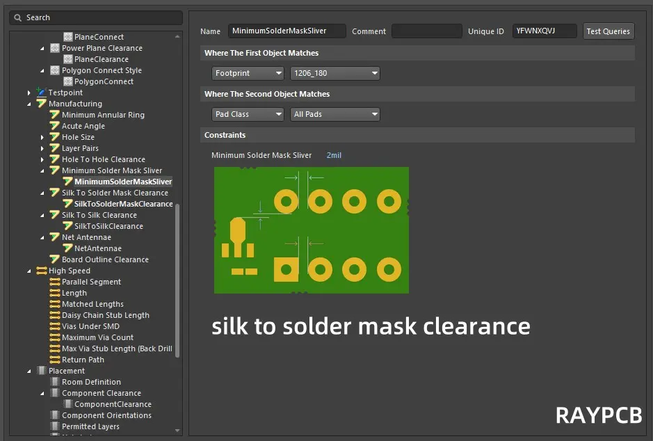
Solder mask clearance refers to the distance between the edge of a copper pad or trace and the edge of the solder mask opening. It’s a critical parameter in PCB design that affects the quality of solder joints, the reliability of connections, and the overall manufacturability of the board.

The Importance of Solder Mask Clearance
Proper solder mask clearance serves several crucial functions:
- Solder Joint Quality: It ensures that there’s enough exposed copper for the solder to adhere to, creating strong and reliable connections.
- Prevention of Solder Bridging: By controlling the flow of solder during the assembly process, it helps prevent unwanted connections between adjacent pads.
- Protection Against Oxidation: It shields the copper traces from environmental factors that could lead to oxidation and degradation over time.
- Manufacturability: It affects the ease with which the PCB can be manufactured and assembled, impacting overall yield.
How Solder Mask Clearance Affects PCB Reliability

The reliability of a PCB is paramount, especially in critical applications where failure is not an option. Solder mask clearance plays a significant role in ensuring this reliability.
1. Solder Joint Strength
Impact of Proper Clearance
- Adequate clearance ensures that solder has enough surface area to form a strong bond with the copper pad.
- It allows for proper wetting of the solder, leading to stronger and more reliable joints.
Consequences of Insufficient Clearance
- Too little clearance can result in weak solder joints that are prone to failure under stress or over time.
- It may lead to incomplete solder coverage, reducing the mechanical strength of the connection.
2. Prevention of Short Circuits
Role of Solder Mask Clearance
- Proper clearance helps maintain isolation between adjacent pads and traces.
- It prevents solder from flowing where it shouldn’t, reducing the risk of short circuits.
Risks of Inadequate Clearance
- Insufficient clearance can lead to solder bridging between nearby pads, causing short circuits.
- It increases the risk of electrical failures and reduces the overall reliability of the PCB.
3. Protection Against Environmental Factors
Shielding Provided by Solder Mask
- The solder mask acts as a protective layer against moisture, dust, and other contaminants.
- Proper clearance ensures that this protection extends to the critical areas around solder joints.
Vulnerability Due to Poor Clearance
- Inadequate clearance can leave copper exposed, making it susceptible to oxidation and corrosion.
- This can lead to degradation of electrical connections over time, reducing the PCB’s lifespan.
4. Thermal Management
Heat Distribution and Solder Mask Clearance
- Proper clearance allows for better heat dissipation during the soldering process.
- It helps prevent localized overheating that can damage components or the PCB itself.
Thermal Stress Due to Improper Clearance
- Insufficient clearance can lead to uneven heating during soldering, potentially causing thermal stress.
- This stress can result in warping of the PCB or damage to sensitive components.
Impact of Solder Mask Clearance on Manufacturing Yield
Manufacturing yield is a critical factor in PCB production, directly affecting costs and efficiency. Solder mask clearance plays a significant role in determining this yield.
1. Solder Paste Application
Optimal Clearance for Stencil Printing
- Proper clearance ensures that solder paste can be accurately applied through stencil printing.
- It allows for consistent solder paste volume across all pads, improving soldering reliability.
Challenges with Improper Clearance
- Too little clearance can lead to solder paste smearing or insufficient deposition.
- Excessive clearance may result in solder paste spreading beyond the intended areas.
2. Component Placement Accuracy
Clearance and Pick-and-Place Machines
- Adequate clearance provides visual and mechanical references for automated pick-and-place machines.
- It helps ensure accurate component placement, reducing the risk of misalignment.
Issues Arising from Poor Clearance
- Insufficient clearance can make it difficult for machines to accurately place components.
- This can lead to misaligned components, resulting in poor solder joints or complete failure to connect.
3. Reflow Soldering Process
Role of Clearance in Reflow Soldering
- Proper clearance allows for optimal solder flow during the reflow process.
- It helps in forming consistent and reliable solder fillets around component leads.
Reflow Challenges Due to Improper Clearance
- Insufficient clearance can lead to solder balling or beading, causing potential short circuits.
- Excessive clearance may result in solder wicking, leading to weak or insufficient joints.
4. Inspection and Quality Control
Clearance and Automated Optical Inspection (AOI)
- Adequate clearance facilitates easier visual and automated inspection of solder joints.
- It allows for clear differentiation between good and potentially problematic connections.
Inspection Difficulties with Poor Clearance
- Insufficient clearance can make it challenging to visually inspect solder joints.
- It may lead to false positives or negatives in automated inspection systems, reducing overall yield.
5. Rework and Repair
Importance of Clearance in Rework Processes
- Proper clearance allows for easier rework and repair of PCBs when necessary.
- It provides space for technicians to access and modify solder joints without damaging surrounding areas.
Rework Challenges Due to Inadequate Clearance
- Insufficient clearance can make rework extremely difficult or impossible.
- It increases the risk of damaging adjacent components or traces during the rework process.
Read more about:
Best Practices for Solder Mask Clearance
To ensure optimal PCB reliability and manufacturing yield, consider the following best practices for solder mask clearance:
1. Follow Industry Standards
- Adhere to IPC standards for solder mask clearance, which typically recommend 50-75 μm (2-3 mils) for most applications.
- Consider stricter clearances for high-reliability or fine-pitch applications.
2. Consider Component Types
- Adjust clearance based on the types of components used (e.g., through-hole vs. surface mount).
- Use larger clearances for components that generate more heat or are subject to mechanical stress.
3. Account for Manufacturing Tolerances
- Include a buffer in your clearance calculations to account for manufacturing variations.
- Consult with your PCB manufacturer to understand their specific capabilities and limitations.
4. Balance Clearance with Other Design Factors
- Consider the relationship between solder mask clearance and other design elements like trace width and spacing.
- Ensure that clearance doesn’t compromise other critical aspects of your PCB design.
5. Use Design Rule Checks (DRC)
- Implement thorough DRC in your PCB design software to catch clearance issues early.
- Regularly review and update your design rules to reflect current best practices and manufacturing capabilities.
6. Prototype and Iterate
- Create prototypes to test your solder mask clearance in real-world conditions.
- Be prepared to iterate on your design based on prototype performance and feedback from manufacturers.
Advanced Considerations for Solder Mask Clearance
As PCB technology advances, there are several emerging considerations for solder mask clearance:
1. High-Density Interconnect (HDI) PCBs
- HDI boards often require tighter clearances due to smaller feature sizes.
- Consider using laser-defined solder mask for highest precision in HDI applications.
2. Flexible and Rigid-Flex PCBs
- Flex PCBs may require larger clearances to account for material movement and stress.
- Consider the impact of bending and flexing on solder mask adhesion and clearance.
3. High-Frequency Applications
- In RF and high-speed digital designs, solder mask clearance can affect signal integrity.
- Consider selective solder mask removal in critical RF areas to optimize performance.
4. Automotive and Harsh Environment Applications
- PCBs for automotive or industrial use may require larger clearances to withstand thermal cycling and vibration.
- Consider using specialized solder mask materials designed for harsh environments.
5. 3D Printed Electronics
- As 3D printed electronics evolve, new considerations for solder mask clearance are emerging.
- Stay informed about developments in additive manufacturing techniques for PCBs.
Conclusion: Balancing Reliability and Yield through Proper Solder Mask Clearance
Solder mask clearance is a critical factor that significantly impacts both the reliability of PCBs and the efficiency of their manufacturing process. By understanding the importance of proper clearance and implementing best practices, PCB designers and manufacturers can:
- Enhance the overall reliability and longevity of their products
- Improve manufacturing yield, reducing costs and time-to-market
- Minimize the risk of field failures and associated warranty claims
- Facilitate easier inspection, rework, and repair processes
As PCB technology continues to evolve, with trends towards miniaturization, higher densities, and more demanding applications, the role of solder mask clearance becomes increasingly critical. Staying informed about industry standards, emerging technologies, and best practices is essential for anyone involved in PCB design and manufacturing.
By paying close attention to solder mask clearance and its impacts, you can ensure that your PCBs meet the highest standards of quality, reliability, and manufacturability. This attention to detail will not only improve your current designs but also position you well for the challenges and opportunities of future PCB technologies.
