
RAYPCB · ENGINEERING REFERENCE
PCB Thermal Resistance: Paths, Assumptions & Calculation Limits
Calculate a declared one-dimensional conduction path from thickness, conductivity and common area. See which layer dominates before expanding the thermal model.
Original engineering guidance · References checked September 29, 2026
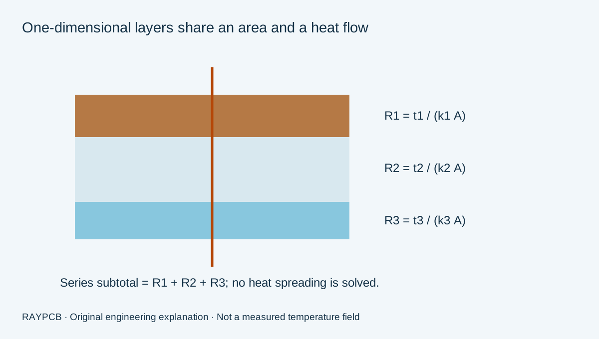
PCB thermal resistance belongs to a defined heat path
PCB thermal resistance describes the temperature difference associated with heat flowing between specified locations under specified conditions. It is normally expressed in kelvins per watt, K/W, numerically equivalent to degrees Celsius per watt for a temperature difference. A value without endpoints, heat-flow allocation and a board configuration is incomplete. There is no single thermal resistance that describes every component, copper pattern and installation on an otherwise identical laminate.
Start with the engineering question: are you estimating conduction across an insulating layer, comparing a component-to-chassis interface, or predicting an operating junction temperature? The first question can sometimes be screened with a simple slab model. The last normally involves the package, multiple board paths, interfaces and the surrounding environment. This page calculates declared conduction terms. The broader PCB thermal design guide connects those terms to a resistance budget and a verification plan.
An early calculation is useful when it exposes a missing thickness, a small contact area or a dominant insulating layer. It becomes misleading when its assumed area silently expands to the full board, when all device loss is assigned to one path without justification, or when an attractive result is treated as a measured product temperature.
The quantities and units must agree
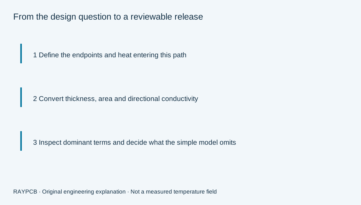
For steady one-dimensional conduction through a uniform layer, R = t/(k A). Thickness t is in metres, conductivity k in W/(m K), and area A in square metres. The temperature difference across that layer is heat rate Q multiplied by resistance R. The worksheet accepts millimetres and square millimetres and performs the conversion: R in K/W = 1000 × t in mm / (k × A in mm²).
| Quantity | Meaning in this calculation | Common source of error |
|---|---|---|
| Thickness | Distance along the modeled heat path | Using overall board thickness for a thin dielectric interface |
| Conductivity | Material value in the heat-flow direction | Substituting in-plane data for through-thickness data |
| Area | Common active cross-section of the ideal path | Substituting total panel area for the local source footprint |
| Heat rate | Power that actually enters the modeled path | Assuming all electrical input becomes heat in one device |
| Additional resistance | Explicitly supplied compatible series term | Inventing a contact value or adding incompatible endpoints |
The difference between thermal conductivity and thermal resistance matters here: conductivity is a material property, while this resistance depends on geometry. Retain the exact material grade and measurement context. A calculation using an assumed conductivity is still an assumption, even if the dimensions came from a released drawing.
Work through a small layered example
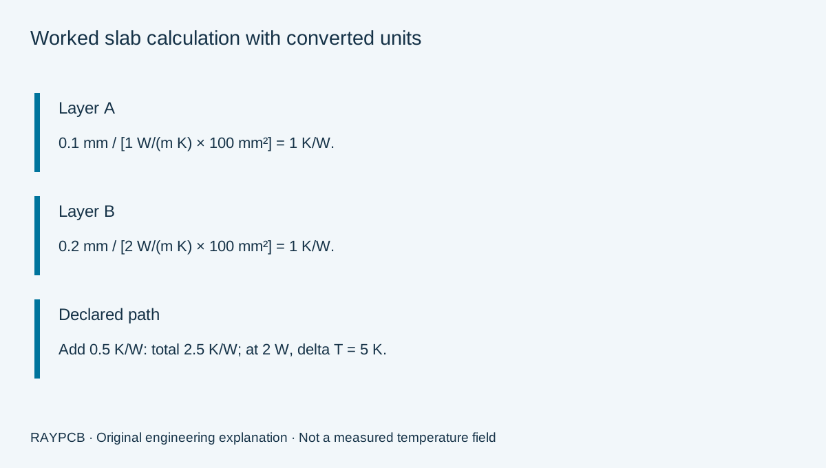
Consider two hypothetical insulating layers sharing an active area of 100 mm². Layer A is 0.1 mm thick with k = 1 W/(m K); its resistance is 1 K/W. Layer B is 0.2 mm thick with k = 2 W/(m K); it also contributes 1 K/W. These are illustrative values, not recommended materials or RAYPCB capability limits.
If an independently justified additional series term is 0.5 K/W, the declared total is 2.5 K/W. At 2 W flowing through that same path, the calculated endpoint temperature difference is 5 K. It is not an absolute temperature. It does not establish the device junction temperature, because the modeled endpoints may be only the top and bottom faces of a local board section.
Doubling the second layer's conductivity would reduce its contribution from 1 to 0.5 K/W. The complete declared total would fall from 2.5 to 2 K/W, a 20% reduction. This is the reason to rank individual terms before buying a more conductive material: a large improvement in one property may produce a modest improvement in the complete path.
Calculate and document a one-dimensional layer stack
Enter one line per layer in the form name, thickness in mm, conductivity in W/(m K). Enter the common area, the heat flowing through the stack and any separately established series resistance. Use zero for that last field only to document that the term has been omitted, not to assert perfect real interfaces. Keep the source or assumption reference with the calculation.
RAYPCB ENGINEERING
Thermal DesignOne-dimensional layer resistance calculator
Loading One-dimensional layer resistance calculator…
The result lists each layer, the conduction subtotal, the added term and the endpoint temperature difference. It identifies the largest layer contribution so you can decide which assumption or construction deserves attention. A named layer is not automatically a different physical material: a copper-bearing equivalent region requires its own justification before it can be entered as a uniform slab.
The tool starts without project values. Its example is explicitly illustrative. Changing an input invalidates the prior result and download, preventing an old brief from being mistaken for a new calculation. Download the current brief locally and attach it manually to an enquiry if useful. The worksheet does not read your board files, transfer attachments to a form or run a three-dimensional solver.
Where the simple slab model stops representing a PCB
A small component usually releases heat into a larger, patterned structure. Copper planes distribute heat laterally, dielectric layers impede some paths, vias provide local connections and board edges or chassis contacts remove heat elsewhere. A common-area series stack omits this spatial behavior. Increasing the entered area can reduce the calculated resistance without creating a corresponding physical path in the product.
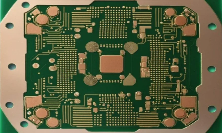
Likewise, a plated via is not simply a solid copper cylinder. Hole-wall plating, filling material, pads, plane attachments and interfaces all affect the path. Use the thermal via design guide to specify the construction and assembly constraints before representing an array in a model. Do not divide a single-via resistance by the via count without checking whether the assumed temperature differences and parallel-path conditions are defensible.
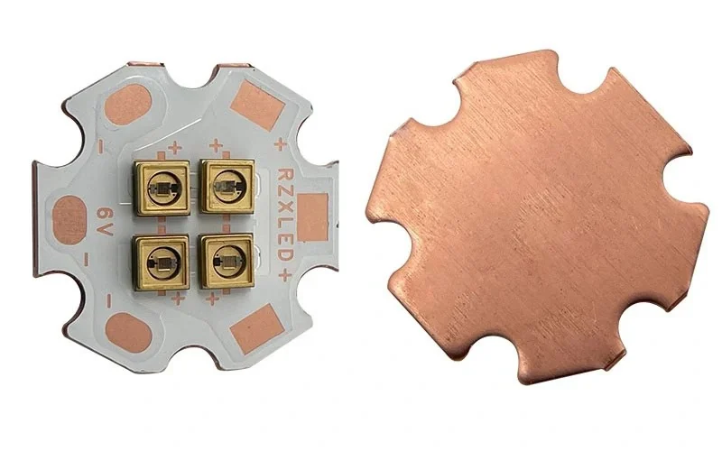
For a metal-core board, the dielectric between circuitry and metal can remain an important term even though the base spreads heat effectively. A board-to-heatsink interface then adds its own area, pressure, flatness and material questions. The metal-core PCB overview addresses that construction choice; this calculation cannot select an insulation system from conductivity alone.
Series and parallel paths need consistent endpoints
Series resistances can be added when the same steady heat flows through the connected terms and their endpoints align. Parallel conductances can be added when the paths connect the same two temperature nodes. In a board assembly, these conditions need a drawing of the thermal network, not just a list of numbers copied from different reports.
For example, a device can release heat through its exposed pad, leads and package surface. The fraction entering the PCB depends on the installed conditions. Assigning the full device loss to both a top-side path and a board-side path double counts power. Conversely, ignoring a real parallel path may make a screening model conservative, but that conservatism should be stated and checked rather than assumed universally.
Do not interchange package metrics with board slab terms. Texas Instruments explains the test-environment dependence of junction-to-ambient metrics and the distinction between resistance and characterization parameters in Semiconductor and IC Package Thermal Metrics. In particular, a characterization parameter such as ΨJT is not an ordinary series resistance that can be inserted into this layer sum.
Convert a prediction into a useful prototype test
Name the modeled endpoints before selecting measurement locations. A surface thermocouple, infrared reading and inferred junction temperature describe different quantities. Record their positions, attachment or emissivity treatment, operating duration and the electrical condition that produces the heat. Do not compare a modeled local hotspot with a measured temperature from an easier but cooler location without explaining the difference.
Also record the mounting state. Open-bench operation, an enclosed product and a clamped board-to-chassis assembly can produce different heat removal. Fan state, orientation, neighbouring components and interface pressure belong in the test description. A calculation that matches one condition should be checked against another relevant load or boundary case before it becomes a reusable design assumption.
If area spreading, several sources or uncertain convection controls the answer, prepare a PCB thermal simulation brief. A more detailed model is valuable when it answers a decision the simple worksheet cannot resolve. Increasing numerical detail without improving input evidence can make a result look more precise without making it more reliable.
Put thermal requirements into the manufacturing discussion
Share the board revision, stackup, finished copper requirements, exact dielectric grade, local dimensions and the intended heat exit. Identify which parameters are controlled requirements and which remain candidate values. If contact to a housing matters, include the relevant mechanical drawing and tolerances; a board supplier cannot infer an assembly contact condition from Gerber data alone.
For PCB manufacturing, ask which proposed material and construction details can be reviewed against the drawing. Request evidence for the property or feature you depend on rather than a generic statement that the board is thermally optimized. A calculation, a material data sheet and an inspection record answer different questions and should remain distinguishable in the release package.
Useful enquiry attachments include the layer calculation, an annotated heat-path sketch and the unresolved questions. A request such as “review this dielectric thickness and the filled-via construction under U3” is more actionable than “make the PCB cooler.” You can send the project requirements directly without completing the worksheet first.
Questions engineers ask about PCB thermal resistance
Can I calculate PCB thermal resistance from board thickness alone?
No. Even the simple slab equation also requires conductivity in the relevant direction and an active area. A practical assembly adds copper pattern, heat spreading, interfaces and environmental conditions. Thickness alone does not define either the heat path or its endpoints.
Does a lower calculated resistance guarantee a lower junction temperature?
Only a model covering the relevant heat generation and paths can support that prediction, and the model still needs verification. Reducing one layer term may help little if another interface dominates or if much of the device heat follows a different route.
Can this worksheet calculate transient temperature?
No. It does not include thermal capacitance, time-dependent losses or temperature-dependent properties. A transient problem needs the appropriate material and operating histories and a model whose time resolution is checked against the behavior of interest.
What should I send when material conductivity is unknown?
Send the exact grade, proposed construction and the thermal question, with the missing property explicitly identified. Avoid substituting a generic value and presenting the result as established. A sensitivity calculation can still show whether resolving that uncertainty is likely to change the design decision.
Bring the heat path and manufacturing requirements together
Send the board revision, construction, quantity and the thermal design question you need reviewed. Identify unresolved requirements so the response can address them.
Send requirements for reviewOptional: attach the downloaded worksheet manually. This guidance does not certify a design, approve a shipment or replace the applicable authorized standards.

