What are Solder Paste Stencils?

LASER STENCIL MANUFACTURER
Solder Paste Stencils

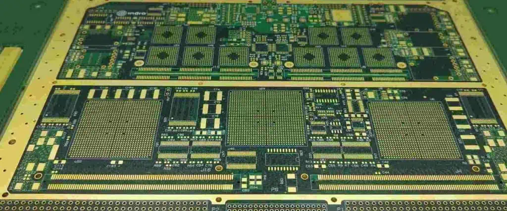
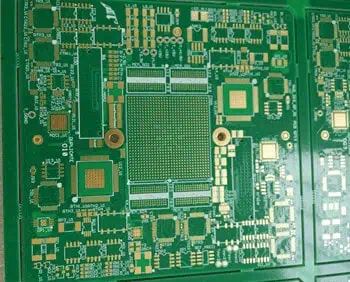
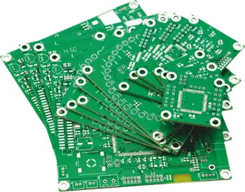
As the electronics technology is advancing, the use of through-hole electronic components is getting out of fashion, and Surface Mount Devices have replaced them. The production of modern components is mostly Surface Mount Technology based.

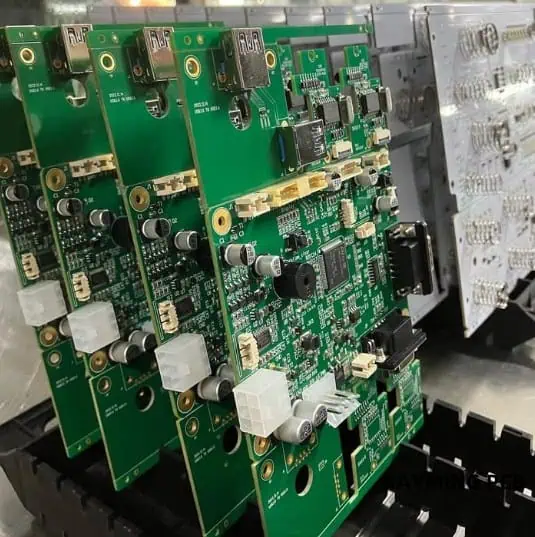
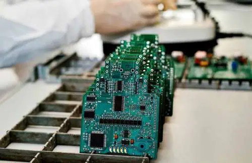
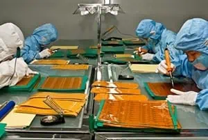
Consequently, many manufacturers prefer using SMDs based products. When it comes to bulk production, manually soldering each board can be hectic and time-consuming. Besides the quality of each joint matters, even a poor joint can trigger malfunctioning in the product.

YouTube video

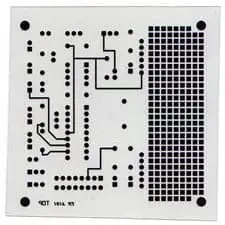
Surface Mount Technology Stencils offer convenience in depositing solder paste within perfect quantity and shape. All you need to do is to set up your board, put some solder paste and swipe it. In case of a single prototype to be developed, using an SMT stencil can be costly and, but for bulk production, SMT stencils can considerably reduce production time and cost.

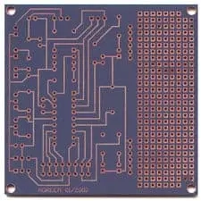
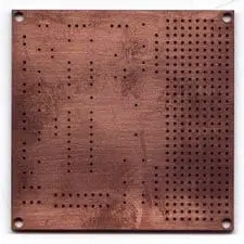
Stencils are usually used in industry for bulk production, and a single stencil can serve thousands of PCBs. However, for few units production, metal stencils can be expensive. For small quantity of units to be produced, polyimide stencils are more suitable. These laser cut stencils works reliably if you are working on a few boards. Since these laser stencils are made of synthetic polymer, and the development cost is low, they are suitable for a limited quantity of boards to be developed.

How are Solder Paste Stencils Designed?

FULL PCB MANUFACTURING Quote

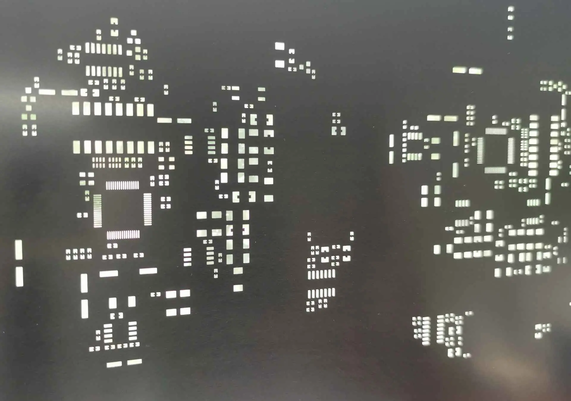
The solder paste stencil is designed using a soft version of the project. During the circuit is designed using any designer software such as Altium, Eagle, DipTrace or Kicad. The soft design includes a layer of solder paste and using this layer machine is instructed to cut holes in exact dimensions are precise locations.

The dimensions and location of each stencil hole determine its efficiency, designing a stencil using original design files of circuit ensure the locations are accurate and the solder paste is deposited in precise dimensions.

Since the solder paste needs to be deposited in a limited region and it can spread slightly out the hole boundaries. To cover up the excessive deposition, the stencil holes are designed a bit smaller the component pads.

How is a Solder Paste Stencil Used?

Using a solder paste stencil is simple and easy. The hardware must be set up properly before deposition, and the PCB needs to be in stationary position, in case of vibrations or movement, the solder paste might be deposited out the pads.

After setting up hardware, the stencil and PCB must be appropriately aligned. The alignment should ensure each solder pad is exposed through the holes of the stencil. Fix stencil on PCB. When aligning the stencil and PCB, look for IC pads, they are easy to track as they have multiple pads.

Carefully verify each pad is exposed through the hole and then put some solder paste on the stencil, using a card, slowly spread solder paste on holes. The paste needs to be spread in all direction to ensure the hole is appropriately covered with paste and the pad is not left uncovered partially.

Solder paste should be used within a few hours of pasting, in case of delay, its efficiency might reduce. Usually, solder paste deposited on stencil is more than needed and the extra paste is used for the next board. It is recommended to use a limited quantity of paste that can be served on a single board.

When the paste has been deposited entirely, remove tapes on the stencil and carefully remove the stencil from the PCB. Inspect each pad, check if the paste has been appropriately deposited. In case, the paste has spread more than needed, it must be removed, and if the paste is missing on any locations, it must be deposited manually.

After the paste is deposited on a PCB, often some paste is left in the stencil holes. This leftover paste is not harmful to the stencil and can be wiped later.

laser cut stencils

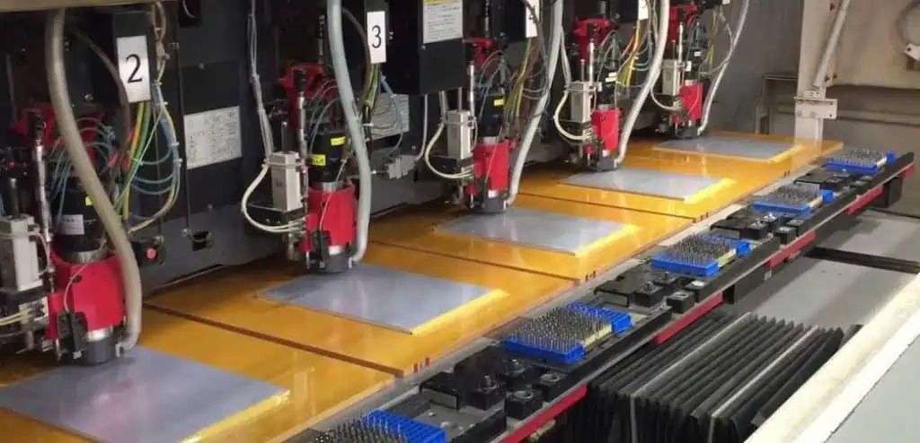
Carefully place all components using SMT pick and place machine, ensure the direction of the component is according to the design. Sometimes, during the placement of components, the component is misplaced or disoriented. Such misplacements can cause improper or no soldering of any legs. In such case, carefully move disoriented component and bring it in a proper place. A minute quantity of paste is often spread around the pad during the replacement. But during heating, this paste reaches back to the pad.

After a detailed examination of each component, the PCB is passed through an oven which heats the board from the top and the paste turns into molten solder. The paste is usually in flat formation before heating but as soon as it is heated, it takes the form of a proper solder joint, and the corresponding componentโ€™s leg is soldered with the pad.

Solder paste deposition demands patience and practice. The procedure is easy, but the process needs to be handled carefully.

Solder Paste Stencils manufacturing at RAYMING

RAYMING is a top notch seller of a variety of solder paste stencils. It doesnโ€™t matter if you belong to a small or large industry with a few or several units order, RAYMING will come up with an affordable offer for you.

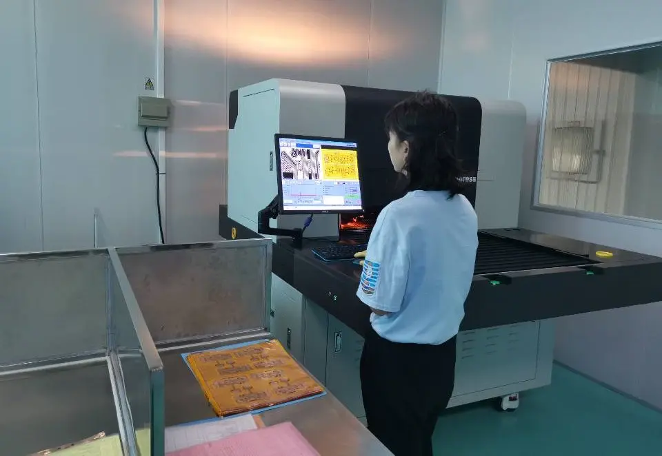
We offer various services related to prototype PCB assembling. The modern technologies and state of the art machinery at RAYMING labs maintain superior quality of our services. So far, we have assisted industries belonging to different segments of the market, and we have developed a name for quality services.

We understand that the product reliability and durability are the core qualities that should not be compromised at any cost. Our automated systems enable us to focus even on microscopic level details of products.

Product development with proper testing makes it reliable and builds the confidence of consumer in using it. We, as a manufacturer of solder paste stencils, test each stencil on our advanced systems and our team ensures the product quality is maintained according to international standards.

RAYMING cares about small industries, and it has played a significant role in uplifting small industries. If you are looking for a PCB stencil manufacturer, share your order details, and we will offer an appealing package.

We are always open to queries, if you need support, contact us at sales@raypcb.com and you will be responded in a short time.

Quick Turn PCB Assembly: Speed Without Compromise

pcb assembly cost down

In today’s fast-paced electronics industry, time-to-market is crucial for staying competitive. Quick turn PCB assembly has emerged as a game-changer, allowing companies to rapidly prototype and produce small batches of printed circuit boards without sacrificing quality. This article delves into the world of quick turn PCB assembly, exploring its benefits, processes, and how to choose the right partner for your needs.

What is Quick Turn PCB Assembly?

Quick turn PCB assembly refers to the rapid production of printed circuit boards, typically for prototyping or small production runs. This service emphasizes speed and efficiency without compromising on quality or reliability. Quick turn assembly involves expedited processes at every stage, from design review to component procurement and final assembly.

Key Features of Quick Turn PCB Assembly:

  • Accelerated turnaround times
  • Flexible production quantities
  • Advanced manufacturing technologies
  • Streamlined communication and project management
  • Rigorous quality control measures

Learn more about:

Benefits of Quick Turn PCB Assembly Orders

Opting for quick turn PCB assembly offers numerous advantages for businesses across various industries. Let’s explore the key benefits:

1. Faster Time-to-Market

In today’s competitive landscape, being first to market can make all the difference. Quick turn PCB assembly significantly reduces production time, allowing you to:

  • Launch products ahead of competitors
  • Capitalize on market opportunities
  • Respond rapidly to customer demands

2. Cost-Effective Prototyping

Quick turn assembly enables efficient prototyping, which can lead to substantial cost savings:

  • Identify and resolve design issues early
  • Reduce the need for multiple revision cycles
  • Minimize waste and material costs

3. Flexibility in Design Iterations

The ability to quickly produce and test prototypes allows for greater flexibility in the design process:

  • Easily implement design changes
  • Experiment with different components or layouts
  • Optimize performance before full-scale production

4. Improved Quality Control

Despite the emphasis on speed, quick turn PCB assembly maintains high-quality standards:

  • Catch and correct errors early in the production process
  • Ensure functionality and reliability of the final product
  • Meet industry-specific quality requirements

5. Enhanced Customer Satisfaction

By reducing lead times and improving product quality, quick turn assembly leads to:

  • Faster delivery of products to end-users
  • Increased customer trust and loyalty
  • Competitive advantage in the market

How to Get Quick Turn PCBAs?

Securing quick turn PCB assembly services involves several key steps:

  1. Prepare Your Design Files: Ensure your PCB design files are complete and error-free.
  2. Choose a Reliable Partner: Select a PCB assembly service provider with a track record of quick turnaround and quality results.
  3. Submit Your Order: Provide all necessary information, including design files, bill of materials (BOM), and any special requirements.
  4. Review and Approve: Quickly review and approve any design for manufacture (DFM) feedback or quotations.
  5. Track Your Order: Stay in close communication with your assembly partner throughout the process.

What is Considered a Quick Turn for PCB Assembly?

The definition of “quick turn” can vary depending on the complexity of the PCB and the capabilities of the assembly partner. However, general guidelines include:

  • Prototypes: 24-72 hours
  • Small Production Runs: 3-5 business days
  • Medium Production Runs: 5-10 business days

It’s important to note that these timeframes can be influenced by factors such as board complexity, component availability, and specific customer requirements.

RAYMING’s Typical Turnaround Time for Quick Turn PCB Assembly

At RAYMING, we pride ourselves on our ability to deliver high-quality PCBAs with industry-leading turnaround times. Our typical quick turn assembly timeframes are:

  • Prototype PCBAs: As fast as 72hours
  • Small Production Runs (1-100 units): 5-8 business days
  • Medium Production Runs (101-500 units): 10-15 business days

These timelines showcase our commitment to speed without compromising on quality or reliability.

Factors that Affect the Turnaround Time of a Prototype

Several factors can impact the turnaround time for quick turn PCB assembly:

1. PCB Complexity

  • Number of layers
  • Board size and shape
  • Component density

2. Component Availability

  • Standard vs. specialized components
  • Lead times for specific parts
  • Alternative component options

3. Assembly Requirements

4. Testing and Quality Assurance

  • Level of testing required
  • Compliance with industry standards
  • Documentation needs

5. Production Volume

  • Prototype vs. small-batch production
  • Scalability of assembly processes

Understanding these factors can help you work more effectively with your assembly partner to achieve the fastest possible turnaround times.

What is the Quick Turn PCB Assembly Process?

The quick turn PCB assembly process involves several key stages, each optimized for speed and efficiency:

1. Design Review and DFM Analysis

  • Rapid assessment of PCB design files
  • Identification of potential manufacturing issues
  • Quick feedback and design optimization suggestions

2. Component Procurement

  • Fast sourcing of required components
  • Utilization of extensive supplier networks
  • Strategic inventory management for common parts

3. PCB Fabrication

  • High-speed PCB manufacturing processes
  • Advanced equipment for quick board production
  • Rigorous quality control checks

4. Component Placement

  • Automated pick-and-place machines for SMT components
  • Skilled technicians for through-hole component insertion
  • Optimized production line setup for efficiency

5. Soldering

6. Inspection and Testing

  • Automated optical inspection (AOI)
  • X-ray inspection for hidden solder joints
  • Functional testing as per customer requirements

7. Quality Assurance and Packaging

  • Final quality checks and documentation
  • Secure packaging for safe transportation
  • Rapid shipping arrangements

By streamlining each of these stages, quick turn PCB assembly providers can deliver high-quality boards in record time.

Choosing the Right Quick Turn Assembly Partner in China

Selecting the right quick turn PCB assembly partner in China is crucial for the success of your project. Consider the following factors:

1. Experience and Expertise

  • Years in the industry
  • Range of PCB assembly capabilities
  • Industry-specific knowledge

2. Technology and Equipment

  • State-of-the-art assembly equipment
  • Advanced inspection and testing technologies
  • Continuous investment in new capabilities

3. Quality Certifications

  • ISO 9001 certification
  • IPC standards compliance
  • Industry-specific certifications (e.g., AS9100 for aerospace)

4. Communication and Customer Service

  • English-speaking support staff
  • 24/7 availability
  • Transparent and responsive communication

5. Flexibility and Scalability

  • Ability to handle various order sizes
  • Quick adaptation to design changes
  • Scalability for future production needs

6. Intellectual Property Protection

  • Robust IP protection policies
  • Confidentiality agreements
  • Secure data handling practices

7. Cost-Effectiveness

  • Competitive pricing
  • Value-added services
  • Transparent quotation process

Why Should You Choose RAYMING as Your Preferred Partner?

RAYMING stands out as a leading quick turn PCB assembly partner in China for several compelling reasons:

1. Unparalleled Expertise

With over 15 years of experience in the PCB industry, RAYMING has developed deep expertise in quick turn assembly across various sectors, including automotive, aerospace, medical, and consumer electronics.

2. Cutting-Edge Technology

We invest continuously in the latest assembly equipment and technologies, ensuring that we can handle even the most complex PCB designs with speed and precision.

3. Rigorous Quality Control

Our ISO 9001-certified facilities and adherence to IPC standards guarantee that every PCBA we produce meets the highest quality standards, regardless of the turnaround time.

4. Customer-Centric Approach

We pride ourselves on our responsive customer service, with dedicated project managers ensuring clear communication and rapid resolution of any issues throughout the assembly process.

5. Flexible and Scalable Services

Whether you need a single prototype or a production run of thousands, RAYMING can adapt to your requirements, providing consistent quality and speed at any scale.

6. Comprehensive Capabilities

From design review to final testing and packaging, we offer end-to-end PCB assembly services, streamlining your supply chain and reducing time-to-market.

7. Competitive Pricing

Our efficient processes and strategic location in China allow us to offer highly competitive pricing without compromising on quality or speed.

Conclusion

Quick turn PCB assembly has revolutionized the electronics manufacturing industry, enabling companies to bring products to market faster than ever before. By choosing the right assembly partner, you can leverage this powerful service to gain a competitive edge, reduce costs, and improve product quality.

RAYMING’s commitment to speed, quality, and customer satisfaction makes us the ideal choice for your quick turn PCB assembly needs. Whether you’re a startup looking to prototype your first product or an established company seeking to optimize your production process, we have the expertise and capabilities to exceed your expectations.

Don’t let slow turnaround times hold your projects back. Experience the RAYMING difference in quick turn PCB assembly today. Contact us to discuss your PCB assembly needs and discover how we can help accelerate your time-to-market without compromising on quality.

What is 3 layer PCB?

double layer pcb circuit board

3 Layer PCB or Three layer PCB Board , Is less in the normally in the market, most most multilayer plural layer like 4 layer , 6 layer, 32 Layer.

Sometime some electronic device need special layer stack up to get the performance , and sometime ,just PCB designer want to save cost , not do 4 layer

RayMing is 3 layer PCB manufacturer ,Welcome to send your design to sales@raypcb.com , We will give your quote asap

Introduction

A printed circuit board (PCB) forms the foundation for building electronic circuits by providing the base for mounting and interconnecting components. PCBs with multiple conductive layers enable increased component density and complex circuit routing. A 3 layer PCB refers to a board with three copper layers separated by insulating dielectric substrates.

This article provides a comprehensive overview of 3 layer PCB technology. We will cover the advantages of 3 layer boards, their construction, common design techniques, applications, and manufacturing considerations. With an understanding of their capabilities and limitations, engineers can effectively utilize 3 layer PCBs in many types of electronic designs.

Advantages of 3 Layer PCBs

Shengyi S1000h PCB

Three layer boards provide the following benefits compared to simpler 2 layer PCBs:

  • Added routing flexibility – The extra layer allows more interconnectivity and circuit optimization. Parts placement and routing are less constrained.
  • Improved signal integrity – The middle layer can be a continuous ground plane. This provides controlled impedance signal routing on outer layers.
  • Lower EMI/noise – Enclosing signals between power and ground layers reduces interference and crosstalk.
  • Better power distribution – Additional layer allows power-ground plane pairs for each voltage domain.
  • Higher component density – Components can be placed on both sides with vertical interconnects through the middle layer.
  • Smaller board sizes – Miniaturization by utilizing both sides for SMT parts placement.
  • Mixed signal designs – Analog and digital sections can be segregated across layers.

For these reasons, 3 layer construction provides excellent capability and cost-benefit for many electronic products.

Construction of 3 Layer PCBs

The fabrication of 3 layer printed circuit boards involves laminating conductive copper layers separated by insulating dielectric substrates:

  • The center substrate is called the core. It provides mechanical support. The default material for core and prepreg layers is typically glass reinforced FR-4.
  • A sheet of copper foil is laminated onto both sides of the core. These form the top and bottom conductive layers of the PCB.
  • Photolithographic processing patterns the copper layers into the required circuit traces, pads, and features.
  • Plated through holes and buried vias provide vertical interconnections between the layers.
  • Soldermask selectively coats the copper layers for protection and isolation.

This creates a 3 layer board ready for component assembly. The sequence can be repeated to build multilayer boards.

Typical 3 Layer Stackups

While all 3 layers can be used for routing signals, some standard layer assignments provide good design starting points:

3 Layer With Ground Plane

  • Layer 1 – Signals
  • Layer 2 – Ground plane
  • Layer 3 – Signals

This offers a continuous reference ground plane for controlled impedance routing and shielding.

3 Layer With Split Power Planes

  • Layer 1 – Signals
  • Layer 2 – Split power planes (VCC and VDD)
  • Layer 3 – Signals

Separate power supply domains can be isolated between the split power planes.

3 Layer With Buried Signal Plane

  • Layer 1 – Ground
  • Layer 2 – Signals
  • Layer 3 – Ground

The buried signal layer fully encompasses routing surrounded by ground planes.

The stackup can be customized based on signal isolation, thermal and EMI requirements.

Design Considerations for 3 Layer Boards

Isola FR406N PCB

Here are some important design practices when working with 3 layer PCBs:

  • Split power planes correctly for digital and analog domains based on current levels.
  • Use a large number of via stitches to connect split power planes for lowest impedance.
  • Assign critical signals to outer layers adjacent to the ground/power planes.
  • Route opposing signal polarities on same layer to minimize crosstalk.
  • Use diagonal routing over middle layer to change layers when needed.
  • Enable thermal relief stitching for highest current paths.
  • Maximize copper area on outer layers for best heat dissipation.
  • Follow adequate design clearances between planes and traces.
  • Model power and ground impedances to avoid resonance and coupling issues.
  • Simulate signal integrity and radiated emissions to high frequencies.

Proper 3 layer stackup design and layout techniques result in schematics which transition smoothly through manufacturing.

Typical Applications of 3 Layer PCBs

Here are some examples of products where 3 layer boards are commonly used:

  • Consumer electronicsIoT devices, smart home gadgets, wearable tech
  • Vehicles – Auto infotainment panels, GPS display units
  • Industrial – PLCs, motor controllers, sensors
  • Instrumentation – Meters, analyzers, handheld testers
  • Medical – Diagnostic equipment, body-worn monitors
  • IT – Ethernet switches, modems, routers
  • Communications – Radio transceivers, video gear

3 layer boards balance cost, complexity and performance for mid-range applications. The proliferation of digital electronics drives large volumes of 3 layer PCBs today.

3 Layer PCB Manufacturing Overview

3 layer PCB fabrication in volume involves the following key steps:

  • Materials – Core substrates, prepreg, copper foils
  • Imaging – Photoresists, direct laser/mechanical patterning
  • Lamination – Stacking layers under heat and pressure
  • Etching – Chemically etching away unwanted copper
  • Drilling – Machines drilling holes for vias and mounting
  • Plating – Electroplating copper over hole walls and surfaces
  • Solder mask – Liquid photoimageable solder resist layers
  • Silkscreen – Printed reference markings
  • Testing – Electrical testing, quality inspection
  • Assembly – SMT component placement and soldering

High-yielding fabrication lines enable cost-effective mass production of 3 layer boards.

Conclusion

With three conductive layers to work with, PCB designers have sufficient flexibility to route out interconnects and partition domains without undue complexity. 3 layer boards offer excellent capability per unit cost, enabling their ubiquity across industrial and consumer electronics. Advances in PCB materials, fabrication equipment and assembly technologies will continue to improve technical features, density and reliability while reducing manufacturing costs.

Frequently Asked Questions

Here are some common questions about 3 layer PCBs:

What are the typical substrate thicknesses used in 3 layer boards?

Standard cores are commonly 0.8mm, 1.0mm, 1.6mm while prepregs range from 0.1mm to 0.25mm. Overall thickness is usually between 1.6mm to 2.4mm.

What are the minimum track/spacing dimensions achievable on 3 layer boards?

With processes like direct imaging, trace/space down to 125um (5 mils) is routinely achievable on outer layers.

What are common 3 layer PCB sizes?

Smaller boards of around 50x50mm to 160x100mm are typical. Large boards up to 460x360mm area are also manufactured cost-effectively.

What are the limitations of 3 layer boards compared to 4+ layer ones?

Design constraints in routing congestion, inability to isolate multiple signals, lower component density and lack of flexibility for high pin-count parts.

What are common materials available for core and prepreg in 3 layer PCBs?

Standard FR-4, High Tg FR-4, Halogen-free FR-4, Rogers materials for high frequency, Polyimide for flexibility, Ceramic-filled substrates for thermal conduction.

High Quality 20 Layer PCB Manufacturer

10 oz pcb circuit board

4.8mm  20 Layer PCB Manufacturing  

RayMing is 20 layer PCB manufacturer ,Welcome to send your 20 layer PCB Design to sales@raypcb.com , We will give the best quote for you .

20-Layer <a href="https://www.raypcb.com/how-to-plan-multilayer-pcb-stackup/">PCB Stackup</a> Selector

20-Layer PCB Stackup Selector 20LULTRA

Configure layer thicknesses for ultra-high-density 20-layer server, HPC, AI accelerator, datacenter switch, and advanced networking PCB designs

Quick Presets

Layer Assignment (10 Signal + 5 GND + 5 PWR)
L1 SIG
L2 GND
L3 SIG
L4 PWR
L5 SIG
L6 GND
L7 SIG
L8 PWR
L9 SIG
L10 GND
L11 PWR
L12 SIG
L13 GND
L14 SIG
L15 PWR
L16 SIG
L17 GND
L18 SIG
L19 PWR
L20 SIG

Copper Layers (20)

Prepreg Layers (10)

Core Layers (9)

Total Board Thickness
3.500mm
3500 ยตm
vs 3.5mm
+0 ยตm
Copper (20L)
700 ยตm
Prepreg (10L)
1310 ยตm
Core (9L)
1600 ยตm
10
Signal
5
GND
5
PWR
8
Stripline
2
Microstrip

Stackup Visualization

L1 – Top SignalSIG 35ยตm
PP1 114ยตm
L2 – GNDGND 35ยตm
Core 1 100ยตm
L3 – SignalSIG 35ยตm
PP2 114ยตm
L4 – PWRPWR 35ยตm
Core 2 200ยตm
L5 – SignalSIG 35ยตm
PP3 114ยตm
L6 – GNDGND 35ยตm
Core 3 200ยตm
L7 – SignalSIG 35ยตm
PP4 114ยตm
L8 – PWRPWR 35ยตm
Core 4 200ยตm
L9 – SignalSIG 35ยตm
PP5 (Center) 185ยตm
L10 – GND (Center)GND 35ยตm
Core 5 (Center) 200ยตm
L11 – PWR (Center)PWR 35ยตm
PP6 185ยตm
L12 – SignalSIG 35ยตm
Core 6 200ยตm
L13 – GNDGND 35ยตm
PP7 114ยตm
L14 – SignalSIG 35ยตm
Core 7 200ยตm
L15 – PWRPWR 35ยตm
PP8 114ยตm
L16 – SignalSIG 35ยตm
Core 8 200ยตm
L17 – GNDGND 35ยตm
PP9 114ยตm
L18 – SignalSIG 35ยตm
Core 9 100ยตm
L19 – PWRPWR 35ยตm
PP10 114ยตm
L20 – Bottom SignalSIG 35ยตm
SOLDER MASK (BOTTOM)
Outer SIG
Inner SIG
GND
PWR
Prepreg
Core
๐Ÿ’ก 20L Targets
3.2mm: High-density HDI
3.5mm: Standard 20L
4.0-4.5mm: Server/HPC
5.0mm+: Backplane
๐Ÿ“ Impedance
Microstrip: L1โ†’L2, L20โ†’L19
Stripline: All inner SIG
Center: L10โ†”L11 tightly coupled
โšก Power Integrity
5 GND: Distributed ref planes
5 PWR: Multi-rail support
L10-L11: Ultra-low Z decoupling
๐Ÿ”Œ Applications
HPC: GPU/TPU accelerators
Network: 400G+ switches
Server: Multi-socket CPU
๐Ÿ”ง 20-Layer Design Strategy
10 Signal Layers: L1, L3, L5, L7, L9, L12, L14, L16, L18, L20 โ€” Ultra-high routing density for complex BGA fanout (0.3mm pitch), HBM3 memory, 224G PAM4 / 112G NRZ SerDes, and PCIe Gen6.
5 GND Planes: L2, L6, L10, L13, L17 โ€” Ground reference within 4 layers of every signal; L10 center GND provides symmetry axis and shielding.
5 PWR Planes: L4, L8, L11, L15, L19 โ€” Support 6+ voltage rails with splits (VCore, VIO, VDDA, VDDQ, VPP, VCCSA); L10-L11 form ultra-low-inductance decoupling pair.
Via Strategy: Requires sequential lamination with blind/buried vias and microvias (stacked or staggered); via aspect ratio typically 12:1 max.
Material: Consider low-loss materials (Megtron 6/7, Tachyon, I-Tera MT40) for high-speed lanes >25Gbps.
Symmetry: Structure symmetric about Core 5 center for optimal CTE matching, warpage control (<0.5%), and reliable BGA/LGA reflow.

20 Layer PCB Stack Up

20 layer PCB

Introduction

20 layer PCBs enable remarkably dense and complex circuit designs for advanced applications. The multilayer board integrates signals, power distribution and components in a compact form factor. However, fabricating 20 layer boards reliably requires expertise in process control and testing. Selecting the right manufacturer is key to ensuring high yields and performance.

This article discusses capabilities required of a high quality 20 layer PCB production facility. We will go over recommendations for stringent process standards, precision equipment, rigorous testing and qualifications needed to deliver complex multilayer boards with high yields and low defects.

Key Capabilities for 20 Layer PCB Fabrication

Producing 20 layer PCBs pushes fabrication equipment and process limits. Here are some must-have capabilities:

  • Handling board sizes exceeding 460mm x 610mm
  • Stackup with 20 conductive copper layers interleaved with dielectric
  • Tight layer to layer registration accuracy of ~50um
  • Line width and spacing down to 3/3 mil with tolerances of +/- 0.5 mil
  • Laser drilled and plated microvias with 5 mil diameter and pitch down to 8 mil
  • 1 oz copper on outer layers, 0.5 oz for inner layers
  • Various dielectric materials – FR4, Rogers, Polyimide, PTFE etc.
  • Sequential lamination with advanced process controls
  • Fine line imaging and etching on inner layers
  • Excellent hole wall plating quality and copper bonding
  • HDI technologies – microvias, stacked vias, blind/buried vias
  • UL, ISO, and other certifications

Fabrication must also assure high yields across large board sizes typical for high layer count.

Critical Process Control Requirements

multilayer pcb manufacturing

Achieving quality and repeatability involves refined process controls:

  • Metrology tools to precisely monitor panel parameters in real-time
  • Maintaining laminate and etchant integrity across long cycles
  • Precise control of lamination temperature and pressure profiles
  • Real-time drilling parameter adjustment – speed, depth, pressure
  • High uniformity copper plating across panel with minimum voids
  • Imaging, etching, stripping processes tuned for high yields
  • Statistical feedback loops for continuous tolerance improvements

Refined process tuning, monitoring and control minimizes scrap and rework even when producing complex stackups.

Advanced Fabrication Equipment Essential

latest equipment allows holding the tight tolerances needed:

  • Direct imaging with 50um lines/spaces rather than using artwork films
  • High accuracy layer-to-layer registration system for stacking and lamination
  • Laser microvia drilling machines with ~5mil capability
  • Advanced plating equipment for uniform copper filling of blind and buried vias
  • Automatic optical inspection systems to detect defects during fabrication
  • Advanced patterning machinery capable of fine features on inner layers

Investment into cutting-edge fabrication tools enables reliable volume production of dense HDI boards.

Comprehensive Testing Is A Must

With the high layer count and complexity, testing assumes even more critical importance:

  • Automated optical inspection after major fabrication steps
  • Netlist testing of bare panels for opens, shorts and impedance
  • Test point integration to enable probing all layers for shorts
  • Microsection analysis of layer alignment, lamination and plated holes
  • Complete functional testing of populated boards
  • In-circuit tests for assembled boards with boundary scan capability

Extensive testing at bare board, assembly and functional stages is essential to achieve final yield targets for 20 layer PCBs.

Qualifications and Certifications

Validated capabilities, quality management and consistency controls differentiate tier-one manufacturers:

  • ISO 9001, ISO 14001 certified facilities
  • IPC 6012 Class 3, IPC 6018 Class 3 qualifications
  • ITAR registration support for defense products
  • UL listing for safety compliance assurance
  • RoHS, REACH, Conflict Minerals compliance
  • Ongoing reliability and improvement testing
  • Statistical process control monitoring

These qualifications provide confidence in their process capabilities and infrastructure.

Finding Reliable 20 Layer PCB Manufacturers

Here are helpful tips when selecting a 20 layer PCB production partner:

  • Review online capabilities – specifically for 20+ layer expertise
  • Validate certifications are current and relevant
  • Ask for customer references with 20 layer boards made
  • Check facilities, equipment investments
  • Review sample quality and test data
  • Have initial engineering discussion – DFM, DFT, capabilities
  • Assess supply chain – inventory, sourcing for prompt delivery
  • Consider locations near your team for operational agility

Taking the time for thorough due diligence during selection ensures you choose the right long-term fabrication partner.

Conclusion

With stringent process controls, advanced fabrication equipment and comprehensive testing, capable manufacturers can reliably produce high-density 20 layer PCBs. Validated infrastructure and certifications provide confidence to take on challenging multilayer builds. Partnering early in design with an experienced 20 layer PCB producer helps navigate design and process complexities for a successful outcome. As electronics innovation pushes further, these partnerships continue enabling intricate products integrating multilayer boards with refined manufacturing.

Frequently Asked Questions

Here are some common FAQs on 20 layer PCB manufacturing:

What are typical 20 layer board thicknesses?

A 20 layer board with standard dielectrics and 1 oz copper can end up around 0.260โ€ (6.6 mm) thickness. Using thinner dielectrics and copper under 0.5 oz reduces thickness.

What line width/space is achievable on 20 layer boards?

Leading manufacturers can achieve 3/3mil line/space on external layers and 5/5mil for internal layers using direct imaging down to 50um resolution.

What materials are used in 20 layer PCB construction?

FR-4 is common for cost-effective boards. High frequency boards use RF materials like Rogers RO4350b or ceramic-filled PTFE. Flexible boards may use polyimide films.

What are the main difficulties in fabricating 20 layer boards?

Maintaining tight layer registration and plating quality through many lamination cycles. Also achieving fine features on inner layers and high yields across large board sizes.

How is component density achieved on 20 layer boards?

High component density is enabled by HDI technologies like microvias, blind/buried vias and thinner dielectrics for routing channels.

Recommended 16 Layer PCB stackup From Manufacturer

16 layer pcb stackup

Rayming Is 16 Layer PCB manufacturer

Material:FR4,TG170 (ITE180).
Thickness: 2.0mm.
min hole: 0.2mm
min trace/space:0.11/0.11mm
200*300 mm per panel ,6 units/panel.
Immersion gold and press fit hole (tolerance 0.05mm)

16-Layer <a href="https://www.raypcb.com/how-to-plan-multilayer-pcb-stackup/">PCB Stackup</a> Selector

16-Layer PCB Stackup Selector 16LPRO

Configure layer thicknesses for enterprise-grade 16-layer server, networking, and AI accelerator PCB designs

Quick Presets

Layer Assignment (8 Signal + 4 GND + 4 PWR)
L1 SIG
L2 GND
L3 SIG
L4 PWR
L5 SIG
L6 GND
L7 SIG
L8 PWR
L9 GND
L10 SIG
L11 PWR
L12 SIG
L13 GND
L14 SIG
L15 PWR
L16 SIG

Copper Layers (16)

Prepreg Layers (8)

Core Layers (7)

Total Board Thickness
2.800mm
2800 ยตm
vs 2.8mm
+0 ยตm
Copper (16L)
560 ยตm
Prepreg (8L)
1142 ยตm
Core (7L)
1200 ยตm
8
Signal Layers
4
GND Planes
4
PWR Planes
6
Stripline

Stackup Visualization

L1 – Top SignalSIG 35ยตm
PP1 114ยตm
L2 – GNDGND 35ยตm
Core 1 100ยตm
L3 – SignalSIG 35ยตm
PP2 114ยตm
L4 – PWRPWR 35ยตm
Core 2 200ยตm
L5 – SignalSIG 35ยตm
PP3 114ยตm
L6 – GNDGND 35ยตm
Core 3 200ยตm
L7 – SignalSIG 35ยตm
PP4 185ยตm
L8 – PWRPWR 35ยตm
Core 4 (Center) 200ยตm
L9 – GNDGND 35ยตm
PP5 185ยตm
L10 – SignalSIG 35ยตm
Core 5 200ยตm
L11 – PWRPWR 35ยตm
PP6 114ยตm
L12 – SignalSIG 35ยตm
Core 6 200ยตm
L13 – GNDGND 35ยตm
PP7 114ยตm
L14 – SignalSIG 35ยตm
Core 7 100ยตm
L15 – PWRPWR 35ยตm
PP8 114ยตm
L16 – Bottom SignalSIG 35ยตm
SOLDER MASK (BOTTOM)
Outer SIG
Inner SIG
GND
PWR
Prepreg
Core
๐Ÿ’ก Common 16L Targets
2.4mm: High-density HDI
2.8mm: Standard 16L
3.2mm: Server/networking
3.5-4.0mm: Backplanes, AI/HPC
๐Ÿ“ Impedance Zones
Microstrip: L1โ†’L2, L16โ†’L15
Stripline: L3,5,7,10,12,14
Tightly-coupled: L8โ†”L9 center
โšก Power Integrity
4 PWR planes: Multiple voltage domains
L8-L9: Low-inductance decoupling
Symmetric: Balanced thermal
๐Ÿ”ง 16-Layer Design Strategy
8 Signal Layers: L1, L3, L5, L7, L10, L12, L14, L16 โ€” Maximum routing density for complex BGA fanout (0.4mm pitch+), DDR4/5, PCIe Gen4/5, and 112G SerDes.
4 GND Planes: L2, L6, L9, L13 โ€” Distributed ground reference every 4 layers minimizes return path inductance and provides EMI shielding.
4 PWR Planes: L4, L8, L11, L15 โ€” Support multiple voltage rails (VCore, VIO, VDDA, etc.); L8-L9 form tightly-coupled power/ground pair for superior decoupling.
Signal Integrity: Every signal layer has an adjacent reference plane within 0.1-0.2mm for controlled impedance. Inner signal layers (L3,5,7,10,12,14) are fully shielded striplines.
Symmetry: Structure is symmetric about Core 4 center axis for optimal CTE matching, warpage control, and reflow reliability.
16 layer pcb

16 Layer PCB Stack Up

16-layer PCB stack up

Introduction

Printed circuit boards with a high layer count are needed for complex, dense electronic designs. 16 layers is typical in many advanced control systems, telecom/networking and medical applications. The layer stackup requires careful planning to optimize electrical performance, thermal management and manufacturability.

This article provides guidelines on how to best use the 16 layers. We discuss recommended approaches for partitioning the layers into signal, ground and power distributions. A sample reference stackup is presented that can be tailored to specific system requirements. We also go over key considerations for 16 layer PCB design and fabrication.

Layer Planning Guidelines

Here are some principles to follow when planning out the layers in a 16-layer board:

  • Split layers evenly between top and bottom of the board for symmetry. This avoids warping.
  • Assign at least 20% layers for ground and 20% for power distribution. This leaves 60% for signals.
  • Place ground and power layers adjacent to signal layers for controlled impedance and decoupling.
  • Locate ground layers outermost as much as possible for easiest routing and heat dissipation.
  • Assign one full uninterrupted ground plane layer on each side adjacent to signal layers.
  • Define several split power planes to isolate analog, digital and high-current power.
  • Order signal layers for optimized grouping based on high-speed, RF or isolated sections of the system.

Using these guidelines results in a versatile stackup suited for mixed-signal, digital and RF system designs.

16 Layer PCB Stackup Example

multilayer pcb design

Here is an example 16 layer stackup designed using the above guidelines:

Layer NumberLayer TypeNotes
1SignalTop-side RF/High-speed signals
2GroundUninterrupted ground plane
3SignalDigital signals
4PowerSplit power planes – 3.3V, 1.2V
5SignalDigital signals
6GroundUninterrupted ground plane
7SignalAnalog signals
8PowerSplit power planes – 5V, 12V
9SignalAnalog signals
10GroundUninterrupted ground plane
11SignalDigital signals
12PowerSplit power planes – 1.8V, 2.5V
13SignalDigital signals
14GroundUninterrupted ground plane
15SignalBottom-side RF/High-speed signals
16GroundUninterrupted ground plane

This stackup ensures:

  • Symmetric top and bottom layer distribution
  • 40% of layers assigned for ground and 40% for various power domains
  • Adjacent ground planes for controlled impedance routing
  • Outer ground planes for easiest heat dissipation and routing
  • Logical grouping of signal layers based on analog, digital, RF domains

The sequence can be modified to suit high density routing requirements and thermal design.

Key Design Considerations

Here are some key points to consider when designing a 16 layer PCB:

  • Via technology – Laser drilled microvias with ~0.2mm holes allow dense interconnections between layers. Backdrilling clears unused sections of vias.
  • Routing channels – Thinner dielectrics like 0.008″ prepregs between layers provide adequate trace routing channels.
  • Controlled impedance – Ground + power layer next to signals allows impedance control for high-speed traces.
  • Decoupling – Multiple power-ground pairs spread across layers provides decoupling capacitors access.
  • Thermal – Thermal reliefs and thermal core layers help conduct heat out from inner layers.
  • Signal integrity – Follow length matching, tuning and crosstalk guidelines for high-speed traces.
  • ** manufacturability** – Work with fabricator early to check DFM, panel utilization, fabrication tolerances.

A disciplined approach is needed when laying out complex 16-layer designs while working closely with the PCB manufacturer to ensure producibility.

Fabrication and Testing Considerations

Here are some key considerations during fabrication and testing of densely packed 16 layer boards:

  • Registration accuracy is critical for drilled holes to match pads across 16 layers when stacking up.
  • Layer alignment must be highly precise over large board sizes typical of 16+ layer PCBs.
  • Uniform heat dissipation across multilayer stackup requires careful processing during lamination.
  • Plating quality and hole wall profiles should be strictly controlled for reliable interlayer connections.
  • Electrical test coverage becomes more extensive with the high node count on large multilayer boards.
  • Impedance control, signal integrity and RF performance testing requires advanced test equipment.

The fabrication facility must have proven experience in manufacturing complicated high layer count PCBs cost-effectively.

Recommendations When Ordering

  • Partner with a fabricator experienced in building 16+ layer PCBs
  • Request pre-DFM analysis before finalizing layer stackup
  • Have quickturn prototypes made to validate design and process before committing to production
  • Understand capabilities – layer tolerance, hole size ranges, line/space etc.
  • Discuss any thermal design and signal integrity validation needs
  • Review test coverage – bare board electrical testing, flying probe, ICT
  • Get recommendations for optimal panel sizes, layout and breakout

Conclusion

multilayer pcb manufacturers

A well-planned layer stackup strategy is key to effectively utilize the routing real-estate available in 16 layer designs. The layer sequence must balance signal routing needs, power distribution, heat dissipation and manufacture-ability constraints. A collaborative approach between designer and fabricator ensures a practical stackup optimized for cost, quality and performance. Rigorous design reviews and testing will validate the complex multilayer implementation before volume production.

Frequently Asked Questions

Here are some common FAQs about 16 layer PCB stackups:

What is a typical thickness for a 16 layer board?

A 16 layer board with standard 1oz copper and 0.008″ dielectric layers will result in a total thickness around 0.25″ (6.5mm). Thinner dielectrics can reduce thickness.

What are thermal cores used for in multilayer PCBs?

Thermal cores made of metallic or ceramic layers buried inside the stackup help conduct heat from inner layers to the board surfaces for efficient cooling.

What is backdrilling of PCB holes?

Backdrilling selectively removes the unused lower portions of through hole vias to avoid trapping heat inside multilayer boards. This improves thermal performance.

What are common dielectric materials used in 16 layer boards?

FR-4 glass epoxy is common. High frequency boards use RF materials like Rogers RO4350b. Flexible boards may use polyimide films. Ceramic filled PTFE substrates aid thermal conduction.

What testing is typically done on complicated multilayer PCBs?

Extensive bare board testing for shorts, opens, impedance control, signal integrity and review of fabrication quality before assembly and functional testing of populated boards.

Printed Circuit Board (PCB) Manufacturing Process: A Step-by-Step Guide

printed circuit board manufacturers

Introduction

In today’s digital age, Printed Circuit Boards (PCBs) are the backbone of nearly every electronic device we use. From smartphones to satellites, PCBs play a crucial role in connecting and supporting electronic components. Understanding the PCB manufacturing process is essential for engineers, designers, and anyone involved in the electronics industry. This comprehensive guide will walk you through the intricate steps of PCB manufacturing, providing insights into the technology, challenges, and best practices in this field.

What is PCB Manufacturing?

YouTube video

PCB manufacturing is the process of creating printed circuit boards that mechanically support and electrically connect electronic components using conductive pathways, tracks, or signal traces etched from copper sheets laminated onto a non-conductive substrate. This process involves multiple steps, combining precision engineering, chemistry, and advanced technology to produce boards that meet the exacting standards of modern electronics.

Learn More about:

Key Aspects of PCB Manufacturing:

  1. Substrate Material Selection: Choosing the right base material, typically FR-4 (a glass-reinforced epoxy laminate).
  2. Copper Layering: Applying thin copper foils to the substrate.
  3. Circuit Design Transfer: Transferring the designed circuit pattern onto the copper layers.
  4. Etching: Removing unwanted copper to create the circuit paths.
  5. Layering: For multi-layer boards, bonding multiple layers together.
  6. Drilling: Creating holes for component connections and vias.
  7. Surface Finishing: Applying protective coatings and final touches.

Now, let’s dive into the detailed steps of the PCB manufacturing process.

PCB Manufacturing Process Guide | RAYPCB Engineering Tools

PCB Manufacturing Process Guide

RAYPCB Engineering Tools

2-Layer PCB Manufacturing Process

The standard PCB manufacturing process for double-sided circuit boards. This process involves creating conductive patterns on both sides of a substrate with through-hole connections.

12
Main Steps
5-7
Days Lead Time
1.6mm
Standard Thickness
FR-4
Base Material
01

Design Data Preparation CAM

Import Gerber files, drill files (Excellon), and perform Design Rule Check (DRC). Generate tooling holes and panelization for efficient production.

Gerber RS-274X format verification
Aperture list validation
Net connectivity check
Minimum spacing: 3mil/3mil typical
02

Material Cutting & Preparation LAMINATE

Cut copper-clad laminate (CCL) to panel size. FR-4 glass epoxy is standard, with copper foil thickness typically 1oz (35ฮผm) or 2oz (70ฮผm).

FR-4 TG130/TG150/TG170 options
Copper weight: 0.5oz to 6oz
Panel size optimization
Surface cleaning & deburring
03

Inner Layer Imaging PHOTOLITHOGRAPHY

Apply dry film photoresist, expose using LDI (Laser Direct Imaging) or conventional exposure with photomask, then develop to create circuit pattern.

Dry film lamination at 105-115ยฐC
UV exposure: 80-120 mJ/cmยฒ
Naโ‚‚COโ‚ƒ developer solution 1%
LDI resolution: down to 2mil
04

Etching CHEMICAL

Remove unwanted copper using chemical etchant (typically CuClโ‚‚ or FeClโ‚ƒ based), leaving only the protected circuit traces. Strip remaining photoresist.

Acidic cupric chloride etchant
Etch factor control: 2.5-3.5
Temperature: 48-52ยฐC
NaOH stripping solution 3%
05

AOI Inspection QUALITY

Automated Optical Inspection to detect opens, shorts, missing features, and other defects before proceeding to drilling.

Multi-angle camera inspection
Defect classification & logging
CAD comparison algorithm
First article inspection (FAI)
06

CNC Drilling MECHANICAL

High-speed drilling for through-holes and component holes using carbide drill bits. Multiple hit counts tracked for tool life management.

Spindle speed: 80,000-200,000 RPM
Min drill size: 0.15mm (6mil)
Position accuracy: ยฑ0.05mm
Entry/exit material backing
07

Electroless Copper Deposition PLATING

Desmear, activate, and deposit thin electroless copper layer (0.5-1ฮผm) on hole walls to establish conductivity for subsequent electroplating.

Permanganate or plasma desmear
Palladium catalyst activation
Formaldehyde reducing agent
Bath temp: 28-32ยฐC
08

Electrolytic Copper Plating PLATING

Build up copper thickness in holes (PTH) and on surface. Target plating thickness typically 20-25ฮผm in holes per IPC-6012 Class 2.

Acid copper sulfate solution
Current density: 15-25 ASF
Throwing power optimization
Pulse plating for high AR holes
09

Solder Mask Application COATING

Apply liquid photoimageable solder mask (LPI/LPISM), expose, develop to protect copper and define solderable areas.

Screen print or curtain coat
Pre-cure: 75ยฐC for 30min
Colors: Green, Black, White, Blue, Red
Final cure: 150ยฐC for 60min
10

Surface Finish FINISHING

Apply protective finish to exposed copper pads. Options include HASL, ENIG, OSP, Immersion Silver, or Immersion Tin based on application.

HASL: Hot Air Solder Leveling
ENIG: 3-6ฮผin Au / 120-240ฮผin Ni
OSP: 0.2-0.5ฮผm organic coat
Lead-free compliant options
11

Silkscreen Legend MARKING

Print component reference designators, logos, and other markings using inkjet or screen printing with epoxy-based ink.

Inkjet printing for fine detail
Min line width: 4mil (0.1mm)
White, Black, Yellow inks
UV cure or thermal cure
12

Electrical Test & Profiling FINAL QC

Flying probe or fixture test for opens/shorts. CNC routing to final board dimensions with V-scoring or tab routing for arrays.

Flying probe: 100% netlist test
Isolation test: >10Mฮฉ
Routing tolerance: ยฑ0.1mm
Final visual & dimensional check

Standard Specifications

  • Board Thickness 0.4-3.2mm
  • Copper Weight 0.5-6 oz
  • Min Trace/Space 3/3 mil
  • Min Drill Size 0.15mm
  • Aspect Ratio 10:1
  • Surface Finish Multiple

Quality Standards

  • IPC-A-600 Acceptability
  • IPC-6012 Qualification
  • IPC-2221 Design
  • UL 94V-0 Flammability
  • RoHS Compliant
  • ISO 9001 Certified

Common Applications

Multilayer PCB Manufacturing Process

Advanced PCB manufacturing for 4+ layer boards requiring lamination of multiple inner layers with prepreg and copper foil. Essential for high-density designs and impedance control.

18+
Main Steps
10-15
Days Lead Time
4-40L
Layer Count
ยฑ0.1mm
Registration
01

Design Review & Stackup Definition ENGINEERING

Define layer stackup, material selection, and impedance requirements. Calculate prepreg/core thicknesses for target impedance values.

Impedance modeling (Si9000/Polar)
Dk/Df material characterization
Signal integrity simulation
Thermal analysis for power planes
02

Inner Layer Core Preparation MATERIAL

Cut thin core laminate (typically 0.1-0.5mm) with copper on both sides. Clean and prepare for imaging process.

Core thickness: 0.05-1.0mm
High-Tg FR-4, Rogers, Megtron
Bake out moisture removal
Chemical cleaning & micro-etch
03

Inner Layer Imaging PHOTOLITHOGRAPHY

Apply photoresist, expose inner layer patterns using high-precision LDI, and develop. Critical for layer-to-layer registration.

Negative-acting dry film
Fiducial mark placement
Registration target exposure
Scale compensation for lamination
04

Inner Layer Etching CHEMICAL

Etch away exposed copper to form inner layer circuitry. Etch factor control critical for fine-pitch designs.

Horizontal conveyorized line
Alkaline or acidic etchant
Line width compensation
Under-etch monitoring
05

AOI Inner Layer Inspection QUALITY

100% automated optical inspection of inner layers before lamination. Defects cannot be repaired after lamination.

Opens/shorts detection
Trace width/spacing measurement
Copper residue inspection
Annular ring verification
06

Oxide/Brown Oxide Treatment SURFACE PREP

Create micro-rough copper surface for enhanced bonding with prepreg during lamination. Black oxide or alternative treatments.

Black oxide (CuO) or brown oxide
Alternative: Organic bond enhance
Pink ring prevention
Surface roughness: Ra 0.3-0.5ฮผm
07

Layup & Registration LAMINATION

Stack inner layers with prepreg sheets and outer copper foil in precise alignment using pins or mass lamination systems.

Pin-lam or mass-lam systems
X-ray registration systems
Prepreg selection per Dk target
Cleanroom environment
08

Vacuum Lamination Press LAMINATION

Apply heat and pressure in vacuum press to cure prepreg and bond all layers into solid multilayer structure.

Temperature: 180-200ยฐC
Pressure: 250-350 PSI
Cycle time: 60-90 minutes
Resin flow control
09

X-Ray Drilling & Target Drill ALIGNMENT

Use X-ray to locate inner layer registration targets. Drill precision tooling holes for outer layer alignment.

X-ray target acquisition
4-point registration calculation
Scale/rotation compensation
Accuracy: ยฑ25ฮผm
10

Mechanical & Laser Drilling DRILLING

Drill through-holes mechanically. Use COโ‚‚/UV laser for blind/buried vias and microvias in HDI designs.

COโ‚‚ laser: 70-150ฮผm vias
UV laser: 25-70ฮผm vias
Aspect ratio up to 15:1
Back drilling for high-speed
11

Desmear & Electroless Copper PLATING

Remove drilling smear from hole walls and deposit seed copper layer for subsequent electroplating.

Plasma or wet chemical desmear
Glass fiber treatment for HDI
Direct metallization option
Interconnect reliability focus
12

Pattern Plating & Etching PLATING

Image outer layers, electroplate copper and tin, then etch to create final outer layer circuit pattern.

Via fill plating for HDI
Pattern copper plating
Tin etch resist plating
Fine-line capability: 2/2 mil
13

Solder Mask, Finish & Test FINAL

Apply solder mask, surface finish, silkscreen. Electrical test with TDR impedance verification for controlled impedance boards.

LDI solder mask imaging
ENIG/ENEPIG for fine-pitch
TDR impedance test
Microsection analysis

Multilayer Capabilities

  • Layer Count 4-40+ layers
  • Min Trace/Space 2/2 mil
  • Laser Via Size 75ฮผm
  • Aspect Ratio 15:1
  • Registration ยฑ2 mil
  • Impedance Tolerance ยฑ10%

Advanced Materials

  • High-Speed Megtron 6/7
  • RF/Microwave Rogers RO4350B
  • High-Tg TG170+ FR-4
  • Halogen-Free Available
  • Low-Dk Dk 3.0-3.5
  • Metal Core Aluminum/Copper

HDI Structures

  • 1+N+1 Standard HDI
  • 2+N+2 Advanced HDI
  • Any-Layer ELIC
  • Via-in-Pad Filled & Capped
  • Stacked Vias Up to 4
  • Skip Vias Supported

Flex PCB Manufacturing Process

Flexible circuit manufacturing using polyimide substrates. Requires specialized handling and processes to maintain dimensional stability and flexibility.

15+
Main Steps
12-20
Days Lead Time
PI
Base Material
1-12L
Layer Count
01

Design Analysis & Material Selection ENGINEERING

Evaluate bend radius, flex cycles, and dynamic vs static flex requirements. Select appropriate polyimide and adhesive system.

Minimum bend radius analysis
DuPont Pyraluxยฎ selection
RA copper for dynamic flex
Adhesiveless vs adhesive-based
02

Polyimide Film Preparation MATERIAL

Cut copper-clad polyimide laminate. Pre-bake to remove moisture and stabilize dimensional properties.

PI thickness: 12.5-125ฮผm
Copper: ED or RA copper foil
Pre-bake: 150ยฐC, 2-4 hours
Carrier frame attachment
03

Drilling & Plasma Desmear DRILLING

UV laser or mechanical drilling for vias. Plasma treatment removes polyimide smear and improves plating adhesion.

UV laser: 25-100ฮผm holes
Oโ‚‚/CFโ‚„ plasma process
Etch-back for reliability
Blind via capability
04

Metallization & Plating PLATING

Electroless copper seeding followed by electrolytic copper build-up. Lower temperatures than rigid PCB processes.

Semi-additive process (SAP)
Sputtering for thin flex
Ductile copper deposit
Lower bath temperature
05

Imaging & Etching PATTERNING

Apply photoresist with scale compensation, expose circuit pattern, and etch with precise control for fine features.

LDI with scale compensation
Fine-line capability: 1/1 mil
Puddle-free spray etching
Etch factor: 3-4 for thin Cu
06

AOI & Coverlay Application COATING

Inspect circuits, then apply polyimide coverlay using vacuum lamination. Critical for flex reliability.

Pre-punched coverlay
Vacuum lamination press
Temperature: 160-180ยฐC
Adhesive flow control
07

Stiffener & Surface Finish FINISHING

Attach stiffeners for component support, apply ENIG surface finish (no HASL due to thermal stress).

FR-4/PI/Metal stiffeners
ENIG most common
PSA or thermoset adhesive
No HASL (thermal stress)
08

Electrical Test & Singulation FINAL QC

Flying probe test with soft probes, laser or die cutting for final profiling, flex cycle testing for critical applications.

Soft-touch probe heads
Laser cutting preferred
Flex life testing
IPC-6013 compliance

Flex Specifications

  • Polyimide Thickness 12.5-125ฮผm
  • Copper Type ED or RA
  • Min Bend Radius 1mm
  • Flex Cycles 1M+ dynamic
  • Min Trace/Space 2/2 mil
  • Operating Temp -200 to 400ยฐC

Material Options

  • Standard PI Kaptonยฎ
  • LCP High-frequency
  • Adhesive Acrylic/Epoxy
  • Adhesiveless Best flex life
  • FR (Flame Retardant) UL 94 VTM-0
  • Coverlay PI + Adhesive

Applications

  • Mobile Devices Smartphones
  • Medical Implants Pacemakers
  • Aerospace Satellites
  • Wearables Smartwatches
  • Automotive Sensors
  • Industrial Robotics

PCB Manufacturing Process Comparison

Compare key differences between 2-layer, multilayer, and flex PCB manufacturing processes to select the right technology for your application.

Process Parameter 2-Layer PCB Multilayer PCB Flex PCB
Base Material FR-4 Glass Epoxy FR-4, High-Tg, Rogers Polyimide (Kaptonยฎ)
Layer Count 2 layers 4-40+ layers 1-12 layers
Lamination Process None (single laminate) Multiple lamination cycles Coverlay lamination
Via Types Through-hole only Through, blind, buried, microvias Through, blind vias
Drilling Method Mechanical CNC Mechanical + Laser UV Laser + Mechanical
Min Trace/Space 3/3 mil (75ฮผm) 2/2 mil (50ฮผm) 2/2 mil (50ฮผm)
Protective Coating LPI Solder Mask LPI Solder Mask Polyimide Coverlay
Typical Lead Time 5-7 days 10-15 days 12-20 days
Key Challenges Limited routing, thermal Registration, impedance control Dimensional stability, handling
Cost Factor 1x (baseline) 2-5x (layer dependent) 3-8x (complexity dependent)
IPC Standard IPC-6012 IPC-6012 IPC-6013
Surface Finish Options HASL, ENIG, OSP, ImSn, ImAg HASL, ENIG, OSP, ENEPIG ENIG, OSP, ImSn (no HASL)

Understanding the PCB Manufacturing Process

The PCB manufacturing process is a complex series of steps that transforms raw materials into functional printed circuit boards. Whether producing simple 2-layer boards, complex multilayer PCBs with high-density interconnects, or flexible circuits for dynamic applications, each technology requires specialized equipment, materials, and expertise.

Key Stages in PCB Board Manufacturing

All PCB fabrication processes share common fundamental stages: design data preparation, substrate preparation, pattern imaging, copper etching, drilling, plating, and surface finishing. However, the specific techniques and equipment vary significantly based on the board type and complexity.

Quality Standards in PCB Fabrication

Professional PCB manufacturers follow strict quality standards including IPC-A-600 for acceptability, IPC-6012 for rigid board qualification, and IPC-6013 for flexible circuit qualification. These standards ensure consistent quality and reliability across the industry.

Choosing the Right PCB Technology

Selection depends on factors including circuit complexity, space constraints, environmental requirements, signal integrity needs, and cost considerations. 2-layer PCBs suit simple designs, multilayer boards enable complex high-speed circuits, and flex PCBs solve space and dynamic flexing challenges.

Ready to Start Your PCB Project?

Get professional PCB manufacturing with fast turnaround, competitive pricing, and engineering support for your 2-layer, multilayer, or flex circuit requirements.

Learn More About PCB Manufacturing Process

PCB Manufacturing Process – 22 Steps

Step 1: Design and Output

The PCB manufacturing process begins with the design phase. Engineers use Computer-Aided Design (CAD) software to create the circuit layout. This design is then converted into a format that manufacturing equipment can understand, typically Gerber files.

Key Points:

  • Circuit schematic creation
  • Component placement and routing
  • Design Rule Check (DRC)
  • Generation of Gerber files and drill data

Step 2: PPE – Pre Production Engineering

Before actual production begins, the design undergoes a thorough review to ensure manufacturability and to identify any potential issues.

Activities in PPE:

  • Design for Manufacturing (DFM) check
  • Stack-up design for multi-layer boards
  • Panelization planning
  • Tool and process selection

Step 3: From File to Film

In this step, the digital design is transferred to a physical film, which serves as a template for creating the circuit pattern on the PCB.

Process Details:

  • Photoplotter usage for film creation
  • Negative or positive image generation based on design requirements
  • Film inspection for accuracy

Step 4: Board Cutting (Copper Clad Laminate Cutting)

Raw PCB material, typically copper-clad laminate, is cut to the required panel size.

Considerations:

  • Precision cutting to ensure correct dimensions
  • Material handling to prevent damage or contamination

Step 5: Printing the Inner Layers

For multi-layer PCBs, this step involves creating the internal circuit layers.

Techniques Used:

  • Photoresist application
  • UV light exposure through the film mask
  • Development of the photoresist

Step 6: Etch Inner Layers

Strip film etching line

Unwanted copper is removed from the inner layers through chemical etching.

Etching Process:

  • Chemical bath application
  • Controlled etching to maintain circuit integrity
  • Removal of remaining photoresist

Step 7: Inner Layer Alignment

Ensuring precise alignment of inner layers is crucial for multi-layer PCBs.

Alignment Methods:

  • Optical alignment systems
  • Registration hole punching
  • Layer stack-up preparation

Step 8: Automatic Optical Inspection (AOI) Inspection

Each inner layer undergoes AOI to detect any defects or inconsistencies.

Inspection Criteria:

  • Circuit pattern accuracy
  • Copper trace width and spacing
  • Absence of shorts or opens

Step 9: Layer-up and Bond

For multi-layer PCBs, the individual layers are stacked and bonded together.

Bonding Process:

  • Layer stacking with prepreg sheets
  • Application of heat and pressure in a lamination press
  • Curing to create a solid multi-layer board

Step 10: Drilling the PCB

Holes are drilled for component leads, vias, and mounting purposes.

Drilling Techniques:

  • CNC drilling for precision
  • Laser drilling for micro vias
  • X-ray drilling for buried vias in multi-layer boards

Step 11: Plating and Copper Deposition

This step involves depositing a thin layer of copper over the entire board, including the drilled holes.

Plating Methods:

  • Electroless copper deposition
  • Electrolytic copper plating
  • Through-hole plating for electrical connectivity

Step 12: Outer Layer Imaging

Similar to inner layer imaging, the outer layer circuit pattern is created.

Imaging Process:

  • Dry film lamination
  • UV exposure using artwork
  • Development of the resist pattern

Step 13: Plating

PCB pattern plating line

Additional copper is plated onto exposed areas to build up the required copper thickness.

Plating Considerations:

  • Copper thickness requirements
  • Uniform plating distribution
  • Plating of surface mount pads

Step 14: Etch Outer Layer

Unwanted copper is removed from the outer layers, leaving the desired circuit pattern.

Etching Techniques:

  • Chemical etching
  • Mechanical etching for fine-line requirements
  • Differential etching for varied copper thicknesses

Step 15: Outer Layer AOI

Another round of AOI is performed to ensure the accuracy of the outer layer circuits.

Inspection Focus:

  • Circuit pattern integrity
  • Copper thickness uniformity
  • Absence of under-etching or over-etching

Step 16: Solder Mask Application

PCB solder mask expose machine

A protective layer is applied to insulate the copper traces and prevent solder bridges.

Solder Mask Process:

  • Solder mask ink application
  • UV curing
  • Development to expose pads and vias

Step 17: Surface Finish

Various finishes are applied to protect exposed copper and enhance solderability.

Common Finishes:

  • Hot Air Solder Leveling (HASL)
  • Electroless Nickel Immersion Gold (ENIG)
  • Immersion Tin
  • Organic Solderability Preservative (OSP)

Step 18: Silkscreen Printing

solder mask screen silk print machine
Solder mask screen silk print machine

Component designators, logos, and other markings are printed on the board.

Silkscreen Considerations:

  • Ink type selection
  • Curing process
  • Alignment with board features

Step 19: Electrical Test

YouTube video

Each board undergoes electrical testing to ensure proper connectivity and isolation.

Testing Methods:

  • Flying probe testing
  • Bed of nails testing
  • Continuity and isolation checks

Step 20: Profiling and V-Scoring

Boards are cut to their final shape, and V-scoring is applied for easy separation of panelized boards.

Profiling Techniques:

  • CNC routing
  • Laser cutting for precision requirements
  • V-groove scoring for break-apart panels

Step 21: Final Inspection

A thorough visual and functional inspection is performed before packaging.

Inspection Points:

  • Physical dimensions
  • Surface finish quality
  • Silkscreen accuracy
  • Overall board integrity

Step 22: Packaging

Boards are carefully packaged to protect them during shipping and storage.

Packaging Considerations:

  • Moisture-sensitive packaging for certain finishes
  • ESD protection
  • Proper labeling and documentation

2 Layer Vs. Multilayer Manufacturing Process

While the basic principles remain the same, there are significant differences between manufacturing 2-layer and multilayer PCBs.

2-Layer PCB Manufacturing:

  • Simpler process with fewer steps
  • No inner layer processing required
  • Generally faster and more cost-effective

Multilayer PCB Manufacturing:

  • More complex with additional steps for inner layers
  • Requires precise layer alignment and bonding
  • Involves advanced techniques for buried and blind vias
  • Offers higher circuit density and better EMI shielding

What is the Difference Between PCB Manufacturing and PCB Assembly Process?

It’s important to distinguish between PCB manufacturing and PCB assembly, as they are two distinct processes in creating a functional electronic device.

PCB Manufacturing:

  • Focuses on creating the bare PCB
  • Involves all steps from design to final board production
  • Ends with a bare board ready for component mounting

PCB Assembly:

  • Begins with a completed bare PCB
  • Involves placing and soldering components onto the board
  • Includes processes like solder paste application, component placement, reflow soldering, and testing of the assembled board

8 Best DFM Tips for PCB Manufacturing

PCB DFM

Design for Manufacturing (DFM) is crucial for ensuring smooth production and high-quality PCBs. Here are eight essential DFM tips:

  1. Optimize Trace Widths and Spacing: Adhere to manufacturer capabilities for minimum trace width and spacing.
  2. Consider Copper Pour: Use copper pours for ground planes and improved thermal management.
  3. Plan Via Placement Carefully: Avoid vias in pads when possible and use appropriate via sizes.
  4. Mind the Edge Clearance: Leave sufficient space between components and board edges.
  5. Use Standard Drill Sizes: Stick to standard drill sizes to reduce manufacturing costs.
  6. Consider Panelization: Design with panelization in mind for efficient production.
  7. Implement Proper Silkscreen Design: Ensure silkscreen text is readable and doesn’t overlap with solder mask openings.
  8. Follow Stack-up Guidelines: Work with your manufacturer to design an appropriate layer stack-up for multilayer boards.

Trends and Challenges in PCB Manufacturing Technology

The PCB manufacturing industry is constantly evolving, driven by advancements in technology and changing market demands.

Current Trends:

  1. Miniaturization: Increasing demand for smaller, denser PCBs.
  2. Flexible and Rigid-Flex PCBs: Growing popularity in wearable and IoT devices.
  3. High-Frequency Materials: Adoption of advanced materials for 5G and high-speed applications.
  4. Additive Manufacturing: Exploration of 3D printing technologies for PCB production.
  5. Green Manufacturing: Focus on environmentally friendly processes and materials.

Challenges:

  1. Increasing Complexity: Managing the complexity of high-density interconnect (HDI) boards.
  2. Material Limitations: Overcoming the limitations of traditional PCB materials.
  3. Cost Pressures: Balancing cost-effectiveness with advanced manufacturing requirements.
  4. Quality Control: Maintaining high quality standards with increasing miniaturization.
  5. Skilled Labor Shortage: Addressing the need for skilled technicians in advanced PCB manufacturing.

Conclusion

The PCB manufacturing process is a complex, multi-step journey that transforms a simple design into a sophisticated electronic component. From the initial design phase to the final packaging, each step requires precision, expertise, and attention to detail. As technology continues to advance, PCB manufacturers must adapt to new challenges while maintaining the high standards of quality and reliability that modern electronics demand.

Understanding this process is crucial for anyone involved in electronics design or production. By following best practices in Design for Manufacturing and staying abreast of industry trends, engineers and manufacturers can ensure the production of high-quality, cost-effective PCBs that meet the ever-evolving needs of the electronics industry.

As we look to the future, the PCB manufacturing process will undoubtedly continue to evolve, driven by the relentless pursuit of smaller, faster, and more efficient electronic devices. The industry’s ability to innovate and overcome challenges will play a crucial role in shaping the next generation of electronic products that will power our increasingly connected world.

What Cost to Make Custom PCB Printing ?

Custom PCB Printing

Introduction to Custom PCB Printing

Printed circuit boards (PCBs) are essential components in almost all modern electronic devices. A PCB serves as the base for mounting and electrically connecting electronic components using conductive tracks and pads. While many electronic devices use mass-produced standard PCBs, custom PCBs allow for optimization and innovation in the design of electronic circuits. Custom PCBs are designed to fit the specific needs of a product.

Custom PCB printing involves designing and manufacturing PCBs tailored to an application. It provides flexibility in terms of the board size, number of layers, components placement, and electrical connections. Though more expensive than using standard PCBs, custom PCB printing enables miniaturization, improved performance, and lower production costs at scale.

This article provides an overview of custom PCB printing costs. We’ll look at the key factors that determine the price of custom PCB production. With an understanding of the costs involved, you’ll be able to budget and plan your custom PCB printing projects.

Key Factors Affecting Custom PCB Printing Costs

Customized rigid flex PCB

Several variables affect the overall cost of custom PCB production. The major factors are:

Size of the PCB

The size of the PCB influences the raw material costs. Larger boards use more base material. Standard PCB sizes range from around 50 x 50 mm up to 460 x 610 mm. Custom PCB projects typically range from a few centimeters on each side up to around 350 x 250 mm.

Number of Layers

Simple PCBs may just have a single conductive layer. However, multilayer boards with 2, 4, 6, or more layers are common. Additional layers increase complexity and material requirements impacting the cost per unit.

PCB Density

The density of components and connections on the board also affects pricing. More densely packed boards take longer to manufacture.

Material Used

The substrate material and copper traces impact costs. Standard glass-epoxy FR-4 boards are inexpensive. Advanced substrates like Rogers, Arlon, and polyimide are costlier. Thicker copper layers add expense.

Quantity

Economies of scale play a major role in pricing. Small prototype volumes are expensive compared to large production runs in the thousands of units.

Manufacturing Tolerances

The complexity of traces and spaces between them determine fabrication tolerances. Tighter tolerances require more careful manufacturing and increase costs.

Lead Times

Rushed turnaround times can command premium pricing. Typical PCB fabrication lead times range from 2 to 10 business days or more.

Certifications

Special certifications like ITAR, UL, or ISO increase production costs due to additional processes and documentation.

Location

Shipping costs from the PCB manufacturer to the customer also impact pricing.

PCB Printing Cost Estimation

Let’s look at how to estimate custom PCB printing costs based on the factors discussed above. We’ll go through examples for simple hobbyist boards and more advanced professional cases.

Two-Layer Board Cost Example

For a simple two-layer board of size 100 x 150 mm built on standard 1.6 mm thick FR-4 substrate with 1 oz copper and green solder mask:

  • Board size: 100 x 150 mm = 15,000 mm^2 or 1.5 dm^2
  • Let’s assume a quantity of 10 pieces
  • Unit cost for small-scale 2-layer PCB with standard FR-4 at 1.6mm thickness and 1 oz copper is around $5 per dm^2
  • Therefore, cost per board = Area x Unit cost x Quantity = 1.5 dm^2 x $5 x 10 = $75
  • Add shipping cost based on location. Within the US, it may be $10-20.
  • Total cost ~ $85-95 for 10 pieces

This cost can be reduced for larger quantities. For example, 100 pieces may only cost $4 per dm^2 bringing the total down to $600.

Four-Layer PCB Cost Example

For a more complex, high-density board with:

  • 4 layers with inner layers used for power and ground planes
  • Dimensions 200 x 150 mm = 30,000 mm^2 or 3 dm^2
  • FR-4 substrate 1.6 mm thick
  • 1 oz copper on outer layers, 2 oz copper for inner layers
  • Black solder mask on both sides
  • Quantity of 25 boards
  • Assume lead time of 5 days
  • Four-layer PCB cost per dm^2 is around $15
  • So cost per board = Area x Unit cost x Quantity = 3 dm^2 x $15 x 25 = $1,125
  • Faster 5-day lead time may add $100-150
  • Shipping within the US ~$30

Total cost ~ $1,255-1,305 for 25 pieces

Again, larger quantities can further reduce the per unit cost.

Multilayer PCB Cost Scaling

As the layer count increases from 2 to 6 or more, here is how PCB cost per dm2 typically scales:

Number of LayersCost per dm2
2 layers$5
4 layers$15
6 layers$25
8 layers$40
10 layers$60

So the cost per unit area increases substantially with more layers due to higher material and manufacturing complexity.

Advanced PCB Material Cost Comparison

Here is a comparison of commonly used advanced PCB substrate materials and how the costs scale relative to standard FR-4 boards:

MaterialCost Scale Factor vs FR-4
FR-41X
Rogers RO4350B~3X
Isola IS680~4X
Arlon 55NT~5X
Polyimide (Kapton)~6X
PTFE~10X

So material choice can significantly impact cost for custom PCB projects. In high-frequency, high-speed, or high-temperature applications, the cost premium for advanced materials may be justified by improved performance.

Online PCB Cost Calculators

rigid-flex pcb fabrication

Many PCB manufacturers provide online cost calculators to estimate prices based on your board specifications. These provide a quick and easy way to budget a custom PCB project.

However, the results may not fully reflect final pricing in all cases. It’s best to contact the PCB company directly with your complete design and requirements for an accurate quotation.

Here are some popular online PCB cost calculators:

  • RayMing PCB
  • Hillmancurtis
  • EuroCircuits
  • ALLPCB

Tips for Cost-Effective Custom PCB Printing

Here are some tips to optimize costs for your custom PCB printing projects:

Carefully Design Within Panel Size

Aim to maximize board size but fit within standard panel dimensions to minimize waste. Common panel sizes are 18×24 inches, 12×18 inches etc.

Combine Multiple Small Boards into a Panel

For small quantity prototype boards, lay out multiple PCB designs within a single panel. This amortizes fixed costs over more boards.

Request Panelizing Service

Some PCB manufacturers can take multiple PCB files and automatically arrange them for cost-effective panelization.

Maximize PCB Density

Optimize component layout and routing to fill the board area, minimizing unused space. This reduces the number of panels required.

Specify Tolerances Sensibly

Use design rules and tolerances just within your assembly requirements. Overly tight tolerances add cost.

Build with Standard Materials

Use common substrates like FR-4 instead of exotic materials for cost-sensitive applications.

Use Plated Half-Holes Instead of Through-Holes

These minimize drilling costs for multi-layer boards while still allowing soldering.

Consolidate Orders

Batch multiple PCB designs together into a single order instead of separate small orders to benefit from volume discounts.

Allow Adequate Lead Time

Standard ~10-day lead time is cost-effective. Rush orders add premium charges.

Compare Multiple Vendors

Shop around and get quotes from several fabricators. Pick the best price for your requirements.

Conclusion

Custom PCB printing provides a versatile option for building specialized electronics hardware. While costs are higher compared to using standard catalog boards, custom PCBs enable optimizing the electronics design for your specific product.

Cost depends on various factors including board size, layer count, manufacturing tolerances and quantity. Following design and ordering guidelines helps manage costs effectively. With the increasing quality of affordable PCB fabrication globally, custom PCB printing makes customized electronics product development accessible to companies and individual makers alike.

Frequently Asked Questions

Here are some common questions about custom PCB printing costs:

What is the typical cost for a simple 2-layer PCB?

For small quantities, a simple 2-layer board costs approximately $5 – $10 per square inch. For larger volumes in the thousands, cost can drop to $1 – $2 per square inch.

Does PCB cost increase linearly with area?

No, PCB cost doesn’t scale linearly with area. There are fixed costs like setup charges, handling, testing etc. So larger boards have a lower cost per unit area.

How much does additional layers add to cost?

Each additional internal layer can increase PCB cost per unit area by $3 – $5 typically. Complex boards with many layers get exponentially more expensive.

When does it make sense to use an advanced PCB substrate?

For simple, cost-sensitive boards FR-4 is fine. For high-speed or high-frequency analog circuits, RF boards, flex PCBs etc, advanced substrates provide better performance despite higher cost.

How can I get an accurate quote for custom PCB fabrication?

Use online estimator tools to get an approximate quote. For accurate pricing tailored to your design, contact PCB manufacturers directly and request a specific quotation.

How to Design a Flexible PCB ?

quick turn flexible PCB prototype

Introduction

Flex Board

A flexible printed circuit board (PCB) is a type of circuit board that can bend and flex. Flexible PCBs allow connections between electronics in situations where rigid boards would be difficult or impossible to use. They are commonly used in consumer electronics, medical devices, aerospace and defense systems, and other applications where flexibility is required.

Designing a flexible PCB requires special considerations compared to rigid PCBs. The flexible substrate material, conductive traces, components, and assembly process need to be selected appropriately to create a functional and reliable flex circuit. This article provides a step-by-step guide on how to design a flexible PCB.

Selecting the Flexible Substrate

Flexible PCB

The flexible substrate, also known as the flex dielectric, is the base material that the conductive traces are printed on. The substrate must be able to withstand bending and flexing without damage. The most common types of flexible substrate materials are:

  • Polyimide (Kapton) – High temperature resistance, excellent chemical resistance, high cost
  • Polyester (PET) – Low cost, moderate temperature resistance
  • Polyamide – High flexibility and tear resistance
  • Fluoropolymer (PTFE) – Excellent chemical resistance, high frequency applications

Polyimide films like Kapton are most widely used due to their combination of electrical, mechanical, and chemical properties. The thickness of the substrate is also an important factor, with common thicknesses ranging from 12.5 to 100 microns. Thinner substrates are more flexible but less durable.

Substrate Thickness Guidelines

ApplicationThickness Range
Consumer electronics25-50 microns
Medical devices50-75 microns
High flex applications12.5-25 microns
Rigid-flex boards50-100 microns

Designing Circuit Traces

YouTube video

The conductive copper traces carry current through the circuit and transmit signals. Traces on flex boards need to be designed to endure continual bending without damage.

Trace Width and Spacing

  • Minimum trace width and spacing is typically 125-150 microns
  • Wider trace widths are needed for higher current carrying applications
  • Traces should not neck down at bending regions
  • Spacing between traces should be increased at fold lines

Trace Routing

  • Traces should follow direction of bend where possible
  • Avoid traces perpendicular to bend axis
  • Use curved traces at bending zones instead of angular traces
  • Stagger traces if crossing bend areas

Pads and Vias

  • Use tear-drop shaped pads at trace ends to relieve stress
  • Pads should be larger than on rigid boards with increased spacing
  • Limit number of vias, use staggered or filled vias at bend areas

Flexible Circuit Components

Flexible Printed Circuit Board

Special consideration is needed when selecting and placing components on a flexible PCB.

Component Types

  • Chip components: Resistors, capacitors, diodes work well
  • Flat components: Ideal for flex circuits to avoid bulges
  • Bare die components: Epoxy encapsulated dice, no packaging
  • Stiffeners: Plates added under components to reduce flexing

Component Placement

  • Place components in areas with minimal bending
  • Use small components to increase flexibility
  • Adhere components with flexible epoxy or solder
  • Avoid placing components where traces change directions

Flex PCB Layer Stackup

flexible pcb circuit board

Flex PCBs typically have a simple single or double sided layer stackup. Complex multilayer flex boards are also possible for dense interconnections.

Single Sided Flex

  • One conductive layer on a flexible dielectric
  • Low cost, simple layout
  • Limited routing capabilities

Double Sided Flex

  • Two conductive layers bonded together
  • Provides additional routing capabilities
  • Allows for crossover traces on two layers

Multilayer Flex

  • Bond dielectric and conductive layers into a multilayer stackup
  • Permits much higher connection density
  • Improves impedance control and cross section
  • Cost increases significantly

Flexible PCB Assembly and Connectors

Specialized assembly methods are required to mount and interconnect components on a flex board.

Assembly Methods

  • Soldering: Requires precise process control to avoid damaging flex substrate
  • Conductive epoxy: Adheres components without reflow or heating
  • Mechanical attachment: Clips, clamps and screws can attach parts

Connectors and Terminations

  • Flex-to-board: Aligns flex PCB traces to a rigid PCB for interconnection
  • ZIF connectors: Zero-insertion force connectors with hinged flex slot
  • Edge card connector: Flex board plugs into card slot on rigid PCB
  • Flat cable: Ribbon cable extends or terminates flex board traces

Flex PCB Design Guidelines Summary

  • Select flexible substrate to meet electrical and mechanical needs
  • Use wide, curved traces spaced appropriately for flexing
  • Carefully place components in least flexing areas
  • Minimize vias, pads and conformal coatings where traces bend
  • Consider special assembly methods like conductive epoxy
  • Incorporate appropriate connectors and terminations

Careful attention during the design process is necessary to create a robust and reliable flexible printed circuit board.

FQA

flexible pcb circuit board

What are the main advantages of flexible PCBs?

Some key advantages of flexible PCBs include:

  • Flexibility – Can bend and flex to fit varied form factors and motions
  • Durability – Withstand repeated bending and flexing without damage
  • Weight savings – Thin, light flexible circuits vs rigid boards
  • Reliability – Dynamic flexing also aids reliability through repeated movement
  • Design freedom – Flexible circuits permit industrial design innovations
  • Ease of assembly – Can integrate interconnections between components

What are some common applications of flexible PCBs?

Flexible PCBs are used in many products where bending, folding, or flexing is required including:

  • Wearable electronics – Fitness bands, smart watches
  • Medical devices – Hearing aids, imaging equipment
  • Consumer devices – Cell phones, cameras
  • Automotive – Sensors, lighting, engine systems
  • Robotics – Arms and joints
  • Aerospace – Satellites, flight systems

What types of substrate materials are used for flex PCBs?

Common flexible PCB substrate materials include:

  • Polyimide (Kapton) – High temp, chemical resist, cost
  • Polyester (PET) – Low cost, moderate temp resistance
  • Polyamide – High flexibility, tear resistance
  • Fluoropolymer (PTFE) – Chemical resist, RF apps
  • Liquid Crystal Polymer (LCP) – High frequency, stiffness

Polyimide is the most widely used due to its superior electrical, mechanical and chemical properties.

How are components assembled on flexible PCBs?

Components can be assembled on flex PCBs using:

  • Soldering – Precision reflow process to avoid damaging flex
  • Conductive epoxy – Cures at lower temps to adhere parts
  • Mechanical attachment – Clips, screws or clamps
  • Socketed mounting – Place ICs in sockets rather than soldering

The assembly method depends on the components used and PCB construction.

What are considerations for flex PCB trace routing?

Guidelines for routing flex PCB traces include:

  • Follow bend direction when possible
  • Minimize traces perpendicular to bend axis
  • Use curved traces at bending zones
  • Increase trace spacing at fold lines
  • Use tear-drop shaped pads at trace ends
  • Stagger traces when crossing bend areas

These methods help relieve stresses from continual flexing and prevent conductor damage.

What substrate is Rogers RT Duroid 5880?

rogers board

Introduction

Rogers RT/duroid 5880 is a popular microwave laminate material used as a substrate for designing high frequency printed circuit boards (PCBs). It is widely utilized in applications like radars, satellite communication, 5G systems, automotive electronics and more.

This article provides an in-depth understanding of Rogers RT/duroid 5880 substrate in terms of its composition, key properties, available forms, typical applications and comparisons with other substrates. We also look at some guidelines for designing with RT/duroid 5880 material.

Composition of Rogers RT/duroid 5880

Rogers RT/duroid 5880 is a ceramic-filled, PTFE (Polytetrafluoroethylene) composite substrate designed for exacting high-frequency circuit applications.

The composite matrix is formed using PTFE polymer with a proprietary inorganic ceramic filler. PTFE provides excellent electrical and mechanical stability across a wide temperature range. The filler allows modifying dielectric properties like permittivity while retaining electrical and thermal performance characteristics of PTFE.

Some key attributes of the composite matrix are:

  • Excellent dielectric constant and loss tangent stability over frequency
  • Low thermal coefficient of dielectric constant for consistent electrical performance
  • Tight control of material properties for consistent circuit response
  • Good flexural strength for thick film metallization and double-sided boards
  • Low Z-axis thermal expansion coefficient

Rogers RT/duroid 5880 material leverages this composite matrix formulation to achieve a unique combination of properties required in high frequency microwave/RF designs.

Dielectric Properties

Dielectric properties are critical parameters that determine how signals propagate in high frequency PCB substrate materials. Rogers RT/duroid 5880 stands out with its stable low-loss dielectric constant over wide frequency ranges.

Some key dielectric properties of RT/duroid 5880 material are:

  • Dielectric constant (er) of 2.2 +/- 0.02
  • Loss tangent (tan ฮด) of 0.0009 at 10 GHz

This provides consistent performance over microwave and mm-wave frequencies, unlike some materials which demonstrate substantial dielectric variation across frequency bands.

The low dielectric constant facilitates better impedance control compared to traditional microwave substrates. The ultra-low loss tangent enables the design of high Q RF circuits.

These stable dielectric properties make RT/duroid 5880 suitable for broad range of microwave and millimeter wave applications.

Rogers RT/Duroid 5880 Calculator | RayPCB Engineering Tools
View RT/Duroid 5880 PCB โ†’

High-Frequency PCB Design Tool

Professional RF/Microwave calculator for Rogers RT/Duroid 5880 substrate. Optimize transmission line designs with precision engineering calculations.

Material Properties

2.20
Dielectric Constant (ฮตr)
@ 10 GHz
0.0009
Loss Tangent (tan ฮด)
@ 10 GHz
1.96
W/mยทK
31
CTE (X/Y Axis)
ppm/ยฐC
2.2
Density
g/cmยณ
260
Max Operating Temp
ยฐC

Standard Substrate Thickness

0.127
mm (5 mil)
0.254
mm (10 mil)
0.381
mm (15 mil)
0.508
mm (20 mil)
0.787
mm (31 mil)
1.575
mm (62 mil)
3.175
mm (125 mil)

Design Calculators

Input Parameters

Calculated Results

Trace Width (W)
1.534mm
Effective Dielectric (ฮตeff)
1.871
Guided Wavelength (ฮปg)
21.93mm
W/h Ratio
3.02
W/h = (8ยทe^A)/(e^(2A)-2) for W/h < 2
A = (Zโ‚€/60)ยทโˆš((ฮตr+1)/2) + ((ฮตr-1)/(ฮตr+1))ยท(0.23+0.11/ฮตr)

Input Parameters

Calculated Results

Trace Width (W)
0.456mm
W/b Ratio
0.449
Zโ‚€ = (60/โˆšฮตr)ยทln(4b/(0.67ฯ€ยท(0.8W+t)))
for W/(b-t) < 0.35

Input Parameters

Calculated Results

Gap Width (G)
0.254mm
Effective ฮตr
1.60
Total Ground Width
1.008mm
Zโ‚€ = (30ฯ€/โˆšฮตeff)ยทK(k’)/K(k)
k = W/(W+2G), ฮตeff = (ฮตr+1)/2

Input Parameters

Calculated Results

Free Space Wavelength (ฮปโ‚€)
30.00mm
Guided Wavelength (ฮปg)
21.94mm
Quarter Wave (ฮปg/4)
5.48mm
Half Wave (ฮปg/2)
10.97mm

Input Parameters

Loss Analysis Results

Dielectric Loss (ฮฑd)
0.042dB
Conductor Loss (ฮฑc)
0.089dB
Total Loss
0.131dB
Loss Rating
โ— Excellent

Design Guidelines

โšก RF Design Rules

  • Maintain consistent trace width for controlled impedance
  • Use 45ยฐ or curved bends (avoid 90ยฐ corners)
  • Keep ground plane continuous under RF traces
  • Add via stitching for ground plane integrity
  • Minimum trace spacing: 3ร— substrate height

๐Ÿ”ง Manufacturing Guidelines

  • Minimum trace width: 0.1mm (4 mil)
  • Minimum spacing: 0.1mm (4 mil)
  • Via diameter: 0.2mm minimum
  • Pad size: Via + 0.3mm annular ring
  • Panel size: Up to 457 ร— 610mm

๐ŸŒก๏ธ Thermal Considerations

  • Max operating temperature: 260ยฐC
  • Tg (Glass transition): >280ยฐC
  • Low CTE mismatch with copper
  • Suitable for lead-free soldering
  • Use thermal vias for heat dissipation

๐Ÿ“Š Performance Tips

  • ฮตr tolerance: ยฑ0.02 for tight designs
  • Use LM version for enhanced stability
  • Edge-coupled designs for tight coupling
  • Grounded coplanar for better isolation
  • Account for frequency-dependent ฮตr

Typical Applications

๐Ÿ“ก

Satellite Communications

Low-loss performance for satellite transponders and LNBs

10 – 40 GHz
๐Ÿ“ฑ

5G mmWave

Antenna arrays and beamforming networks

24 – 39 GHz
๐ŸŽฏ

Radar Systems

Military and automotive radar applications

1 – 77 GHz
๐Ÿ”ฌ

Test & Measurement

High-precision test fixtures and standards

DC – 110 GHz
๐Ÿ›ฉ๏ธ

Aerospace & Defense

Avionics and EW systems

1 – 94 GHz
๐Ÿ“ป

Point-to-Point Links

Microwave backhaul and wireless bridges

6 – 80 GHz

Material Comparison

Property RT5880 FR-4 RO4003C RO3003
Dielectric Constant (ฮตr) 2.20 4.5 3.38 3.00
Loss Tangent (tan ฮด) 0.0009 0.020 0.0027 0.0013
Max Frequency 77+ GHz ~3 GHz ~40 GHz ~40 GHz
Cost High Low Medium Medium-High
Best For High-freq RF Digital/Low-freq Mixed signal Automotive radar

RayPCB Engineering Tools โ€” Professional RF/Microwave PCB Design

Need a quote? Visit RAYPCB Rogers 5880 PCB

Disclaimer: Calculations are for reference only. Verify with EM simulation tools.

RayMing 2 Layer Rogers rt duroid 5880 PCB 2.2 Dielectric Constan

RayMing 2 Layer Rogers rt duroid 5880 PCB 2.2 Dielectric Constan

Original price was: $650.00.Current price is: $625.00.

2 Layer Rogers rt duroid 5880 PCB 1.mm Thickness Dielectric Constan: 2.2 Size: 100×100 mm Rogers 5880 datasheet RT-duroid 5870 – 5880 Data Sheet What is Rogers RT/duroid 5880 ? Rogers RT/duroid 5880 is a high-performance laminate material designed for use in demanding circuit board applications, such as those found in communication systems, radar applications,…

Electrical and Mechanical Properties

YouTube video

In addition to the exceptional dielectric performance, RT/Duroid 5880 exhibits several other useful electrical and mechanical characteristics:

Electrical Properties

  • Volume resistivity - 1 X 10¹⁴ ohm-cm typical
  • Surface resistivity - 5 X 10¹⁴ ohms typical
  • Dielectric strength - 3.0 x 10⁶ V/m typical

Mechanical Properties

  • Flexural strength - 20,000 psi (138 MPa) typical
  • Tensile strength - 10,000 psi (69 MPa) typical
  • Compressive strength - 30,000 psi (207 MPa) typical
  • Density - 2.2 g/cm3 nominal
  • Maximum continuous use temperature - 170ยฐC
  • Decomposition temperature - >280ยฐC
  • Thermal conductivity - 0.71 W/m/K
  • Coefficient of thermal expansion - 17 ppm/ยฐC
  • Young's modulus - 540 ksi (3716 MPa)
  • Poisson's ratio - 0.17
  • Water absorption - <0.02%

This combination of electrical stability, mechanical rigidity, dimensional stability, thermal conductivity and low expansion behavior makes Rogers RT/duroid 5880 a strong candidate for high reliability RF/microwave PCB applications.

Available Forms

Rogers RT/duroid 5880 laminate is commercially available in sheet stock and roll stock forms in a range of thicknesses.

Sheet Stock

Available sheet sizes:

  • 12 x 18 inches
  • 18 x 24 inches
  • 24 x 36 inches

Standard thicknesses:

  • 0.005 inches
  • 0.010 inches
  • 0.015 inches
  • 0.020 inches
  • 0.025 inches
  • 0.030 inches
  • 0.060 inches
  • 0.125 inches

Other custom thicknesses can also be procured.

Roll Stock

Available roll widths:

  • 12 inches
  • 24 inches
  • 48 inches

Standard roll lengths are 250 feet (76 m)

Thickness range:

  • 0.005 inches to 0.062 inches

This wide range of sheet and roll sizes along with various thickness options allows designers to choose the right RT/duroid 5880 laminate form suited for their PCB fabrication process.

Bonding to Other Layers

Rogers RT/duroid 5880 laminate can be bonded using either fusion bonding or adhesive bonding techniques to manufacture multilayer boards.

Fusion Bonding

Multiple layers of RT/duroid 5880 material can be fused together into a monolithic structure without adhesives under heat and pressure. This creates a void-free interface for optimum electrical and mechanical performance.

Fusion bonding allows fabricating multilayer circuits with:

  • High bond strengths > 2000 psi
  • No delaminations or outgassing issues
  • Thinner and lighter assemblies
  • Simplified fabrication without adhesive handling

Adhesive Bonding

RT/duroid 5880 layers can also be bonded using Rogersโ€™ own RO4000 or RO3000 series bondply adhesives. Thermoset polyimide or epoxy films like FR-4 can also be used.

Adhesive bonding provides high flexibility for:

  • Combining dissimilar dielectrics
  • Bonding to metal layers or heat sinks
  • Selective bonding in multilayers
  • High yield for complex circuit stacks

Rogers offers a wide range of adhesive options for integration with RT/duroid 5880 material.

Typical Applications

Some typical applications leveraging Rogers RT/duroid 5880 material include:

  • Radar Systems - Used in radar antennas, phased arrays, T/R modules, filters etc. due to its stable electrical performance and low loss.
  • Military & Aerospace Electronics - Utilized in avionics systems, satellite payloads, flight termination systems requiring reliable high frequency boards.
  • Wireless Communications - Employed in 5G NR base stations, small cells, test equipment and broadband communication systems.
  • Automotive Radar - Used for radars in autonomous vehicles, collision detection and other applications given its thermal and mechanical stability.
  • High-Speed Digital Circuits - Leveraged in very high speed digital applications up to 20+ Gbps like SERDES, interfaces and interconnects.
  • Medical Electronics - Used in RF ablation, MRI coils, and imaging systems given its durability and biocompatibility.

How does RT/duroid 5880 Compare to Other Substrates?

Rogers RT/duroid 5880 provides a beneficial combination of electrical and mechanical characteristics. Here is how it compares with some other common microwave substrate materials:

SubstrateDielectric ConstantLoss TangentKey Features
RT/duroid 58802.200.0009Ultra-low loss, stable dielectric
RT/duroid 60022.940.0012Higher permittivity, low loss
Nelco 4000-13SI3.660.0021Low cost, moderate performance
Rogers RO30033.000.0013Solid all-round performance
Rogers RO4003C3.380.0027High frequency, low loss
Taconic RF-60A6.150.0028Higher permittivity
Rogers TMM10i9.800.0020High dielectric constant

RT/duroid 5880 provides the best combination of low dielectric constant and ultra-low loss tangent enabling exceptional performance in high Q, low loss microwave circuits.

Design Guidelines

Here are some key guidelines to follow when designing PCBs using Rogers RT/duroid 5880 material:

  • Stackup Design - Use symmetric constructions with balanced lamination ratios to minimize warpage. Follow Rogers' guidelines for layer counts, grain direction and lamination sequences.
  • Trace Width and Spacing - Maintain at least 3x dielectric thickness spacing between conductors for leakage control. Use wider lines on outer layers if higher current capacity is needed.
  • Impedance Control - The stable dielectric properties help maintain tight impedance tolerances. But allow for +/- 8% fabrication tolerance.
  • Signal and Power Integrity - Leverage Rogers' material models for simulation. Use sufficient decoupling and maintain isolation from noisy digital circuits.
  • Thermal Management - RT/duroid 5880's thermal conductivity helps heat spreading. Use thermal vias under hot components. Allow sufficient air flow.
  • Fabrication Considerations - Specify workmanship, lamination cycles, drill/rout tolerances etc. clearly. Use Rogers certified circuit facilities.

Following Rogers' guidelines and best practices for the material ensures optimum board performance.

Rogers RT/duroid 5880 - Frequently Asked Questions

rogers 5880 4350 4003 pcb

Here are some common questions around Rogers RT/duroid 5880 high frequency laminate material:

Q1. Can Rogers RT/duroid 5880 material be used for multilayer PCBs?

Yes, RT/duroid 5880 laminates can be fabricated into multilayer PCBs using fusion bonding as well as adhesive bonding techniques. Fusion bonding using multiple sheets of RT/duroid 5880 provides highest performance while adhesive bonding offers more flexibility. Rogers offers compatible bonding adhesives like RO4000 and RO3000 series for multilayer boards using RT/duroid 5880.

Q2. Is Rogers RT/duroid 5880 an RF material?

Yes, RT/duroid 5880 is specifically designed as an RF/microwave substrate with excellent high frequency characteristics. Its stable low dielectric constant and ultra-low loss tangent make it suitable for a wide array of RF applications like radars, 5G, satellite communication, automotive sensors etc. It maintains consistent performance across microwave and mmWave bands.

Q3. Can Rogers RT/duroid 5880 be used for flex PCB applications?

RT/duroid 5880 material is too rigid for fabricating flex PCBs which require highly flexible substrates. While it provides good flexural strength, it is not suited for continuous flexing applications. Rogers FlexWave series of polyimide substrates would be a much better fit for high frequency flex PCB needs.

Q4. Is RT/duroid 5880 suitable for space and aerospace applications?

Yes, RT/duroid 5880 is an ideal aerospace grade material. Its stable electrical properties under varying temperature/humidity, mechanical rigidity, dimensional stability, low outgassing and high reliability make it suitable for mission-critical space applications like satellites, flight systems, launch vehicles etc. leading companies regularly utilize RT/duroid 5880 for aerospace PCB needs.

Q5. What are the pros and cons compared to FR-4 material?

Pros vs FR-4:

  • Far more stable electrical properties under temperature variations
  • Extremely low loss for high Q RF circuits
  • Better impedance control thanks to consistent dielectric constant
  • Withstands higher temperatures than FR-4
  • Lower moisture absorption

Cons vs FR-4

  • Significantly more expensive
  • Special material certification and handling requirements
  • Fabrication limited to Rogers approved circuit shops
  • Overkill for many commercial grade PCB needs

So RT/duroid 5880 provides major advantages for mission-critical, high-reliability microwave and mm-wave boards but with higher cost. FR-4 may be adequate for many commercial grade digital and analog PCB needs.

Rogers RO4350B Datasheet and Dielectric Constant for PCB Use

rogers board

Rogers RO4350B is a popular high frequency circuit board laminate designed for performance-demanding wireless and radar applications from 500 MHz to 77 GHz. This guide provides a detailed overview of RO4350B material properties, key datasheet parameters, design considerations, and dielectric constant specifications that engineers need to know when designing with this high speed PCB substrate.

Rogers RO4350B Overview

Rogers RO4835 PCB

RO4350B is a ceramic-filled PTFE composite laminate reinforced with woven glass fabric. It was engineered by Rogers Corporation specifically to meet the needs of high frequency and high data rate PCB applications.

Some key attributes that make RO4350B suitable for RF and microwave boards include:

  • Stable dielectric constant of 3.48
  • Low loss tangent of 0.0037
  • Tight ฮตr and Dk tolerances
  • Low Z-axis CTE for reliability
  • High thermal conductivity
  • Lead-free compatible processing
  • Excellent mechanical strength
  • Good chemical resistance
  • UL 94 V-0 flame rating

RO4350B achieves an optimal balance of electrical, thermal, and mechanical properties for precision RF circuit fabrication. Let’s look closer at the RO4350B datasheet specs.

RO4350B Datasheet Parameters

YouTube video

Here are some of the most important characteristics and parameters from the Rogers RO4350B datasheet for PCB design and fabrication:

ParameterValue
Dielectric Constant (ฮตr)3.48
Loss Tangent0.0037
Dielectric Toleranceยฑ0.05
Dk Toleranceยฑ0.002 (up to 10 GHz)
Z-Axis CTE41 ppm/ยฐC
XY CTE17 ppm/ยฐC
Tg280ยฐC
Td340ยฐC
Dissipation Factor0.0019 (10 GHz)
Breakdown Voltage1.5 kV/mil
Thermal Conductivity0.69 W/m/K
Moisture Absorption<0.2%
Copper Peel Strength1.3 lb/in
Surface Resistivity1.5 x 10^13 ohm
Volume Resistivity1 x 10^15 ohm-cm
Lead-Free Process260ยฐC Max

These parameters highlight why RO4350B is advantageous for controlled impedance RF boards. Let’s look deeper at some key material properties.

Dielectric Constant and Loss Tangent

Rogers RO4534

The dielectric constant (Dk) indicates how much capacitance a material generates relative to air. Loss tangent quantifies signal loss.

RO4350B provides a stable Dk of 3.48 from 500MHz to over 40GHz with minimal variation versus frequency. This allows engineers to design controlled impedance transmission lines and matching networks that work consistently across the entire frequency range with excellent loss characteristics.

The low loss tangent of 0.0037 ensures minimal signal attenuation as RF energy propagates through the board. It remains under 0.004 up to 77GHz.

Tight Dielectric Tolerances

In addition to stable Dk over frequency, RO4350B also provides tight lot-to-lot dielectric constant tolerances of ยฑ0.05. The variance in Dk from panel to panel is very consistent.

This makes it easier for designers to account for material variations during layout and ensures stable performance across fabricated boards. Tighter ฮตr tolerance provides more margin for meeting impedance targets.

Low Z-Axis CTE

RO4350B has a low coefficient of thermal expansion (CTE) along the z-axis of 41 ppm/ยฐC. This provides reliability by minimizing dimensional changes and movement of dielectric layers during thermal cycling.

High z-axis CTE can lead to copper cracking on inner signal layers which limits board lifetimes. RO4350B resists plating separations and electrical opens caused by excessive z-axis expansion and contraction.

High Thermal Conductivity

With a thermal conductivity of 0.69 W/m/K, RO4350B provides good heat spreading in the dielectric layers to prevent component hot spots. This helps maintain signal fidelity and component lifetime at high RF power levels.

Lead-Free Compatibility

RO4350B is compatible with lead-free soldering processes up to 260ยฐC, meeting the processing needs for modern electronics assembly and manufacturing.

The stable dielectric and low expansion minimizes electrical and physical changes even through multiple reflow cycles at high temperatures.

Excellent Mechanical Strength

The woven glass fabric reinforcement in RO4350B gives the laminate excellent dimensional stability and flexural strength while maintaining low CTE and loss. It also resists microcracking or fracturing during fabrication and assembly handling.

RO4350B Material Grades

Rogers RO4700 PCB

Rogers offers several grades of RO4350B for applications ranging from low cost commercial usage to high reliability aerospace and defense:

  • RO4350B High Reliability (HR) โ€“ For mission-critical aerospace apps
  • RO4350B High Frequency (VF) – For 77GHz mmWave designs
  • RO4350B Low Dk – Minimizes loss tangent
  • RO4350B Bondply – Adhesiveless multilayers
  • RT/duroid 5870 – Low cost version

Consult Rogers to determine the optimal RO4350B variant for your specific RF performance, cost and reliability requirements.

RO4350B Design Considerations

Here are some key design practices engineers should follow when working with RO4350B material:

  • Use impedance calculators like Saturn PCB Toolkit to determine stripline dimensions
  • Account for frequency-dependent Dk in models
  • Include pad and anti-pad shapes in impedance calculations
  • Model discontinuities like stubs, vias, and bends
  • Use teardrop pads on vias for reliability
  • Minimize dielectrically exposed copper for lowest loss
  • Watch for resin starvation, voids and thickness variations
  • Limit glass weave skew to under 5 degrees
  • Allow for Dk and etch tolerances in impedance budgets

Paying attention to these factors when designing on RO4350B ensures stable electrical performance that matches simulations and measurements.

Typical RO4350B PCB Applications

Some common applications leveraging Rogers RO4350B laminate include:

  • 5G NR base stations and user equipment
  • Radio transceivers and receivers
  • Satellite communication systems
  • Wireless infrastructure
  • Radar and automotive sensors
  • Test and measurement equipment
  • Aerospace and defense electronics
  • High speed data links and backplanes
  • Medical diagnostic devices

Its stable dielectric properties and low loss make RO4350B a top choice for reliable wireless and high frequency boards.

Comparing RO4350B to Other Popular RF Laminates

ParameterRO4350BRO4835RO4003CArlon 85N
Dielectric Constant3.483.383.553.5
Loss Tangent0.00370.00310.00270.0025
Dk Toleranceยฑ0.05ยฑ0.05ยฑ0.079ยฑ0.05
Z-Axis CTE41 ppm/ยฐC52 ppm/ยฐC60 ppm/ยฐC20 ppm/ยฐC
Lead-Free Process260ยฐC288ยฐC260ยฐC280ยฐC
CostMediumLowMediumHigh

RO4350B provides the best overall balance at moderate cost. But alternative laminates may be optimal for specific applications.

Availability of RO4350B Material

Rogers Corporation partners with authorized laminators worldwide to stock various thicknesses of RO4350B cores and prepregs. Common offerings include:

  • 0.005โ€ฒโ€ฒ โ€“ 0.062โ€ฒโ€ฒ dielectric thicknesses
  • Prepregs with 106-211 glass styles
  • Copper foil bonds from 0.5 to 3 oz.
  • Isola 370HR resin system
  • Panels and cut sheets
  • Quick-turn lead times

Work with your PCB manufacturer to ensure availability and consistent supply of RO4350B material tailored to your board thickness and copper weight needs.

FQA about Rogers RO4350B Laminates

Rogers-RO3035-pcb

What is the z-axis CTE of RO4350B?

RO4350B has a low z-axis CTE of 41 ppm/ยฐC which minimizes dimensional changes through temperature excursions to avoid reliability risks.

Can Rogers RO4350B be used at frequencies above 10 GHz?

Yes, RO4350B provides stable dielectric performance up to at least 40 GHz. The VF version extends the upper frequency range to 77GHz and beyond.

Does Rogers RO4350B meet UL flammability ratings?

RO4350B achieves a UL 94 V-0 rating for flame resistance meeting safety requirements for consumer and industrial electronics.

What is the breakdown voltage of Rogers RO4350B?

RO4350B has a high breakdown voltage of 15 kV/mil minimizing risk of electrical punch-through in thin dielectric layers.

Can Rogers RO4350B laminates withstand lead-free soldering?

Yes, RO4350B remains stable through lead-free reflow profiles up to 260ยฐC and multiple soldering cycles.

Conclusion

Rogers RO4350B circuit board laminate provides an ideal microwave substrate solution for precision RF circuits up to 77GHz needing stable dielectric properties and low loss. Its tight tolerances, high thermal conductivity, lead-free process capability, and strong mechanical properties make RO4350B a versatile high frequency PCB material. Careful modeling of impedances and discontinuities when designing on RO4350B results in repeatable RF performance across fabricated boards. For wireless systems requiring precision electrical properties at microwave frequencies, RO4350B delivers.