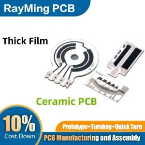
Introduction to Ceramic PCBs
Ceramic PCBs (Printed Circuit Boards) have revolutionized the electronics industry with their exceptional thermal conductivity, superior electrical insulation, and strong corrosion resistance. These unique properties make ceramic PCBs ideal for demanding applications involving high temperatures, high frequencies, and high power.
In this comprehensive guide, we’ll explore the ceramic PCB manufacturing process in detail, providing insights into how these advanced circuit boards are made and why they’re gaining popularity in various industries.
Learn more about:
- PCB Manufacuring Process
- Flex PCB Manufacturing Process
- Rigid Flex PCB Manufacturing Process
- Flex PCB Assembly
- Aluminum PCB Manufacturing Process
Understanding Ceramic PCBs

What Are Ceramic PCBs?
Ceramic PCBs are circuit boards that use ceramic materials as the base substrate instead of traditional materials like FR-4 (fiberglass-reinforced epoxy laminate). The most common ceramic materials used in PCB manufacturing are:
- Alumina (Al2O3)
- Aluminum Nitride (AlN)
- Beryllium Oxide (BeO)
Advantages of Ceramic PCBs
The ceramic PCB manufacturing process results in boards with several advantages over traditional PCB materials:
- Excellent Thermal Conductivity
- High Temperature Resistance
- Superior Electrical Insulation
- Low Dielectric Constant
- Dimensional Stability
- Chemical Resistance
Applications of Ceramic PCBs
Due to their unique properties, ceramic PCBs find applications in various industries:
- Aerospace and Defense
- Automotive (especially in electric vehicles)
- High-frequency RF and Microwave Circuits
- LED Lighting Systems
- Medical Devices
- Power Electronics
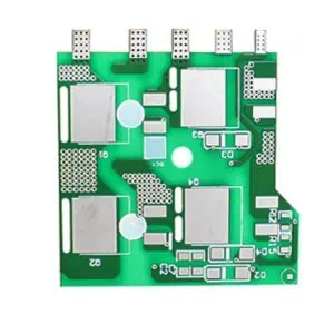
The Ceramic PCB Manufacturing Process: Step by Step

Let’s dive into the detailed ceramic PCB manufacturing process, which requires precision and expertise to produce high-quality, reliable circuit boards.
1. Material Selection and Preparation
Selecting the Ceramic Material
- Alumina (Al2O3): Most common, balances cost and performance
- Aluminum Nitride (AlN): Higher thermal conductivity, more expensive
- Beryllium Oxide (BeO): Highest thermal conductivity, but toxic when processed
Preparing the Ceramic Substrate
- Powder Preparation
- Mixing
- Tape Casting
- Drying
2. Via Formation
Types of Vias in Ceramic PCBs
- Punched Vias
- Laser-Drilled Vias
Via Formation Process
- Designing Via Patterns
- Punching or Drilling
- Via Filling
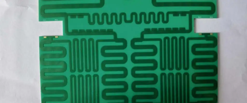
3. Metallization
Metallization Techniques
- Screen Printing
- Thin Film Deposition
- Thick Film Technology
Metallization Process
- Pattern Design
- Paste Preparation
- Screen Printing
- Drying
4. Lamination
Lamination Process
- Layer Alignment
- Stacking
- Pressing
- Pre-Firing
5. Surface Finish
Chemical plating with gold or silver to enhance solderability.
6. Laser Profiling
Using lasers to profile the PCB outline.
7. Electrical Testing
Testing Procedures
- Continuity Testing
- Insulation Resistance Testing
- High-Potential (Hi-Pot) Testing
- Functional Testing
8. Final Inspection and Packaging
Final Quality Control
- Visual Inspection
- Dimensional Verification
- X-Ray Inspection
Packaging
- Cleaning
- Moisture-Proof Packaging
- Shock-Resistant Packaging
Types of Ceramic PCB Manufacturing Processes
1. Thin Film Circuit Process

Key Steps in Thin Film Process
- Magnetron Sputtering
- Pattern Lithography
- Dry/Wet Etching
- Electroplating
Direct Plate Copper (DPC) Variation
2. Thick Film Circuit Process

- a. High-Temperature Co-fired Ceramic (HTCC)
- b. Low-Temperature Co-fired Ceramic (LTCC)
- c. Direct Bonded Copper (DBC)
3. LAM Technology Process

Key Features of LAM Technology
- High Bonding Strength
- Excellent Conductivity
- Customizable Metal Layer Thickness
- High Resolution
- Superior Thermal Management
Advantages of LAM Technology
Comparison of Ceramic PCB Manufacturing Processes
| Process | Resolution | Thermal Performance | Cost | Typical Applications |
|---|---|---|---|---|
| Thin Film | Highest (< 10 μm) | Good | High | RF/Microwave, High-Density Interconnect |
| Thick Film (HTCC/LTCC) | Moderate (50-100 μm) | Very Good | Moderate | Multi-layer designs, Sensors |
| DBC | Low (> 100 μm) | Excellent | Low | Power Electronics, LED Lighting |
| LAM | High (10-20 μm) | Excellent | High | Aerospace, Advanced Power Modules |
Choosing the Right Ceramic PCB Manufacturing Process
Factors to consider:
- Application Requirements
- Design Complexity
- Production Volume
- Budget Constraints
- Environmental Conditions
Challenges in Ceramic PCB Manufacturing
- High Processing Temperatures
- Material Shrinkage
- Cost
- Limited Repairability
- Brittleness
Future Trends in Ceramic PCB Manufacturing
- 3D Printing
- Nano-Ceramic Materials
- Green Manufacturing
- Integration with Flexible Electronics
- AI and Machine Learning
Conclusion: The Growing Importance of Ceramic PCBs
As electronic devices become more powerful and are used in increasingly demanding environments, the role of ceramic PCBs continues to grow. Their unique combination of thermal management, electrical performance, and reliability makes them indispensable in cutting-edge applications.
Understanding the ceramic PCB manufacturing process is crucial for engineers and designers looking to push the boundaries of what’s possible in electronic design. While challenges remain, ongoing research and technological advancements are continuously improving the manufacturing process, making ceramic PCBs more accessible and versatile.
As we look to the future, ceramic PCBs will undoubtedly play a pivotal role in enabling the next generation of high-performance electronic devices, from advanced aerospace systems to revolutionary medical technologies. The ceramic PCB manufacturing process, with its precision and complexity, stands as a testament to human ingenuity in the ever-evolving world of electronics.